Intersil Corporation ICL7663S Datasheet

ICL7663S
Data Sheet April 1999
CMOS Programmable Micropower
Positive Voltage Regulator
The ICL7663S Super Programmable Micropower Voltage
Regulator is a low power, high efficiency positive voltage
regulator which accepts 1.6V to 16V inputs and provides
adjustable outputs from 1.3V to 16V at currents up to 40mA.
It is a direct replacement for the industry standard ICL7663B
offering
improved
coefficient,
guaranteed line and load regulation. All improvements are
highlighted in the electrical characteristics section.
parameters are guaranteed over the entire commercial
and industrial temperature ranges.
programmableoutputvoltageis set bytwo external resistors.
The 1% reference accuracy of the ICL7663SA eliminates the
need for trimming the output voltage in most applications.
The ICL7663S is well suited for battery powered supplies,
featuring 4µA quiescent current, low V
output current sensing and logic input level shutdown
control. In addition, the ICL7663S has a negative
temperature coefficient output suitable for generating a
temperature compensated display drive voltage for LCD
displays.
wider
operating voltage and temperature ranges,
output accuracy (ICL7663SA), bettertemperature
guaranteed
maximum supply current, and
Critical
The ICL7663S/SA
IN
to V
OUT
differential,
File Number
3180.3
Features
•
Guaranteed
10µA Maximum Quiescent Current Over
Temperature Ranges
Wider
•
•
Operating Voltage Range - 1.6V to 16V
Guaranteed
Operating Temperature Range
Line and Load Regulation Over
Optional
Entire
• 1% Output Voltage Accuracy (ICL7663SA)
• Output Voltage Programmable from 1.3V to 16V
Improved
•
Temperature Coefficient of Output Voltage
• 40mA Minimum Output Current with Current Limiting
• Output Voltages with Programmable Negative
Temperature Coefficients
• Output Shutdown via Current-Limit Sensing or External
Logic Level
• Low Input-to-Output Voltage Differential
• Improved Direct Replacement for Industry Standard
ICL7663B and Other Second-Source Products
Applications
• Low-Power Portable Instrumentation
• Pagers
All
Ordering Information
TEMP. RANGE
PART NUMBER
ICL7663SCBA 0 to 70 8 Ld SOIC (N) M8.15
ICL7663SCPA 0 to 70 8 Ld PDIP E8.3
ICL7663SACBA 0 to 70 8 Ld SOIC (N) M8.15
ICL7663SACPA 0 to 70 8 Ld PDIP E8.3
ICL7663SIBA -25 to 85 8 Ld SOIC (N) M8.15
ICL7663SIPA -25 to 85 8 Ld PDIP E8.3
ICL7663SAIBA -25 to 85 8 Ld SOIC (N) M8.15
ICL7663SAIPA -25 to 85 8 Ld PDIP E8.3
(oC) PACKAGE PKG. NO.
• Handheld Instruments
• LCD Display Modules
• Remote Data Loggers
• Battery-Powered Systems
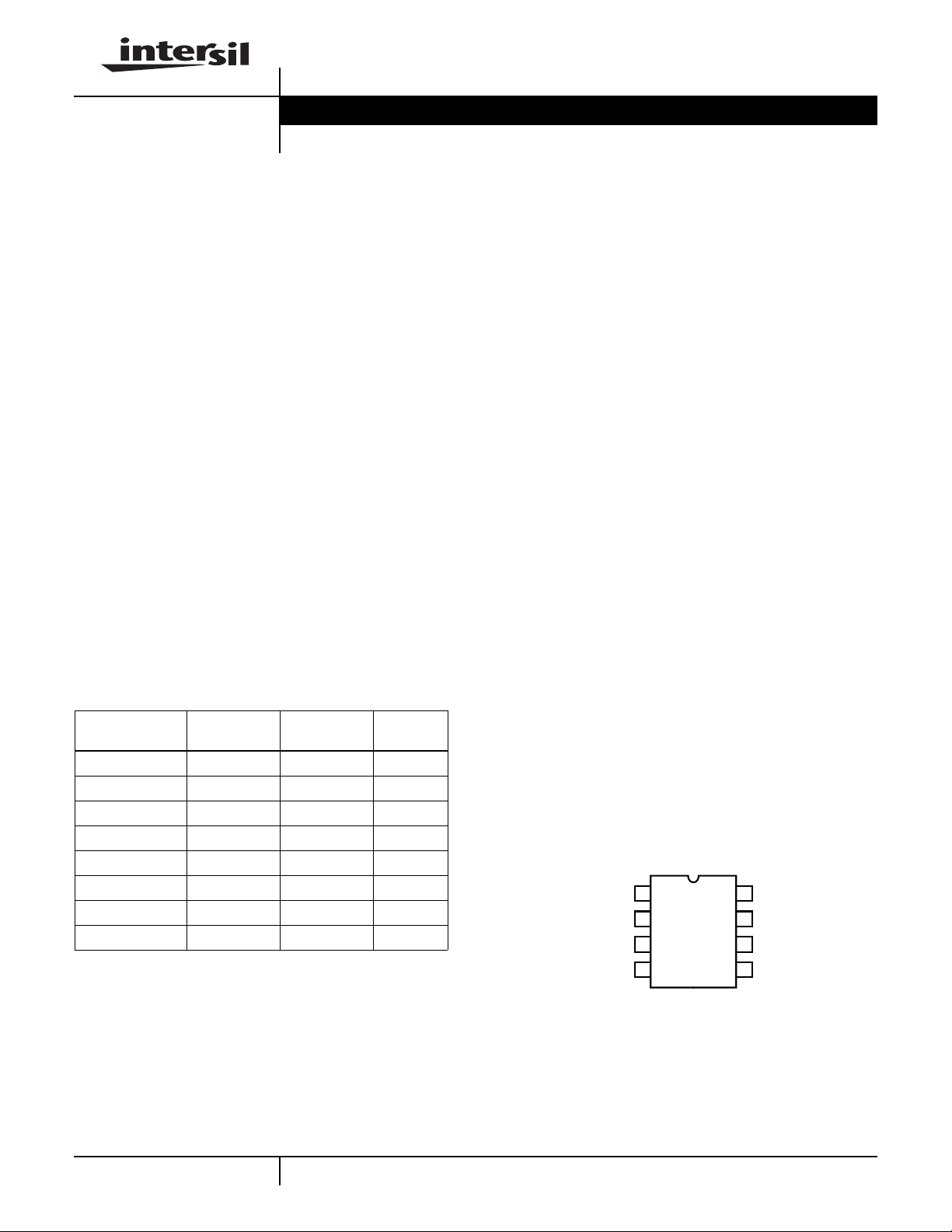
Pinout
ICL7663S
(PDIP, CERDIP, SOIC)
TOP VIEW
V
OUT2
V
OUT1
GND
1
2
3
4
SENSE
8
7
6
5
VIN+
V
TC
V
SET
SHDN
3-55
CAUTION: These devices are sensitive to electrostatic discharge; follow proper IC Handling Procedures.
http://www.intersil.com or 407-727-9207
| Copyright © Intersil Corporation 1999

ICL7663S
Absolute Maximum Ratings Thermal Information
Input Supply Voltage . . . . . . . . . . . . . . . . . . . . . . . . . . . . . . . . +18V
Any Input or Output Voltage (Note 1)
Terminals 1, 2, 3, 5, 6, 7. . . . . . . . . . . . . VIN+ 0.3V to GND -0.3V
Output Source Current
Terminal 2. . . . . . . . . . . . . . . . . . . . . . . . . . . . . . . . . . . . . . . 50mA
Terminal 3. . . . . . . . . . . . . . . . . . . . . . . . . . . . . . . . . . . . . . . 25mA
Output Sinking Current
Terminal 7. . . . . . . . . . . . . . . . . . . . . . . . . . . . . . . . . . . . . . -10mA
Operating Conditions
Temperature Range
ICL7663SC. . . . . . . . . . . . . . . . . . . . . . . . . . . . . . . . . 0oC to 70oC
ICL7663SI . . . . . . . . . . . . . . . . . . . . . . . . . . . . . . . -25oC to 85oC
CAUTION: Stresses above those listed in “Absolute Maximum Ratings” may cause permanent damage to the device. This is a stress only rating and operationofthe
device at these or any other conditions above those indicated in the operational sections of this specification is not implied.
NOTES:
1. Connecting any terminal to voltages greater than (V+IN + 0.3V) or less than (GND - 0.3V) may cause destructive device latch-up. It is recommended that no inputs from sources operating on external power supplies be applied prior to ICL7663S power-up.
2. θJA is measured with the component mounted on an evaluation PC board in free air.
Thermal Resistance (Typical, Note 2) θJA (oC/W) θJC (oC/W)
CERDIP Package. . . . . . . . . . . . . . . . . 115 30
PDIP Package . . . . . . . . . . . . . . . . . . . 150 N/A
Plastic SOIC Package . . . . . . . . . . . . . 180 N/A
Maximum Junction Temperature
PDIP Package . . . . . . . . . . . . . . . . . . . . . . . . . . . . . . . . . 150oC
CERDIP Package. . . . . . . . . . . . . . . . . . . . . . . . . . . . . . . 175oC
Maximum Storage Temperature Range. . . . . . . . . . -65oC to 150oC
Maximum Lead Temperature (Soldering 10s) . . . . . . . . . . . . .300oC
(SOIC - Lead Tips Only)
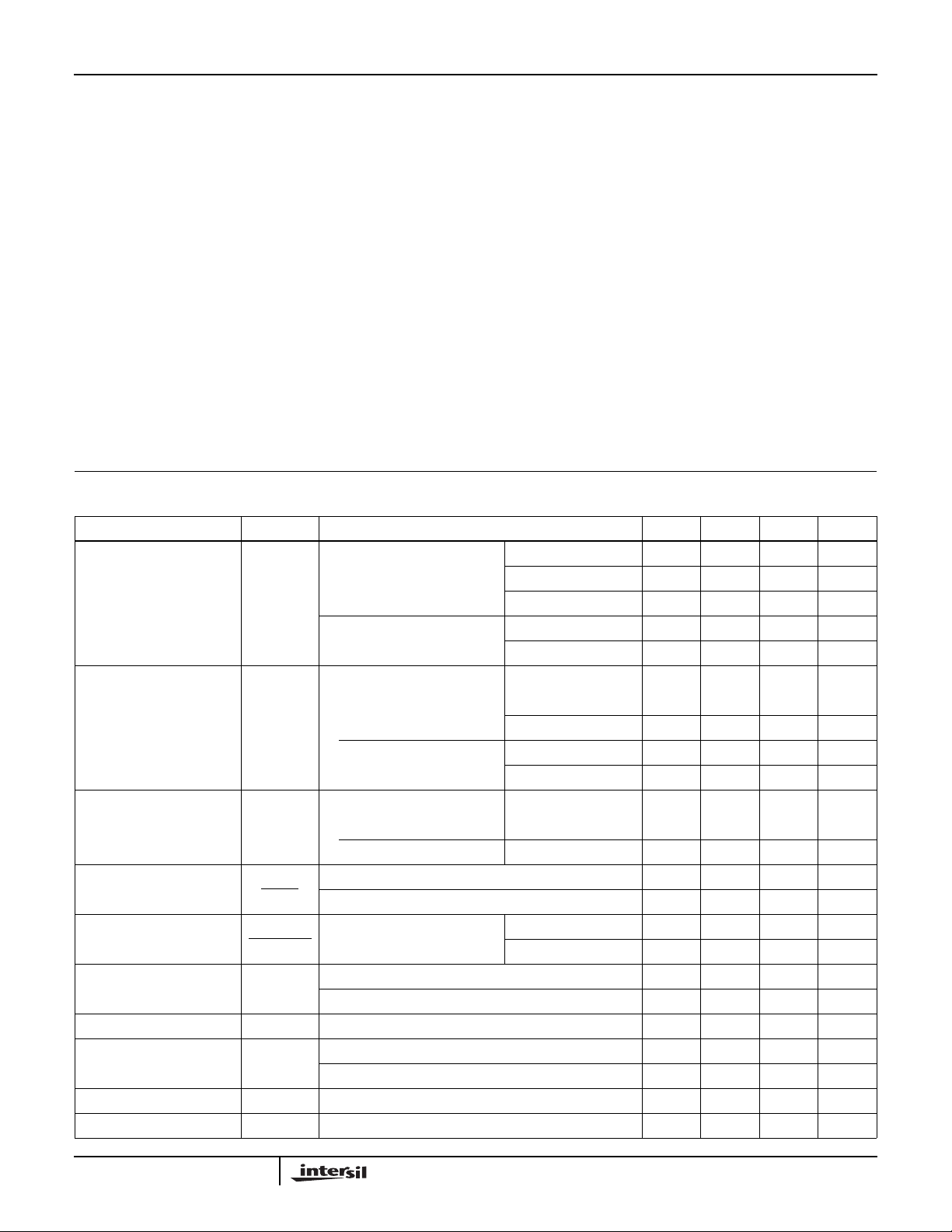
Electrical Specifications Specifications Below Applicable to Both ICL7663S and ICL7663SA, Unless Otherwise Specified. V+
V
= 5V, TA = 25oC, Unless Otherwise Specified. Notes 4, 5. See Test Circuit, Figure 7
OUT
PARAMETER SYMBOL TEST CONDITIONS MIN TYP MAX UNITS
Input Voltage V+
Quiescent Current I
Reference Voltage V
Temperature
∆V
Coefficient
Line Regulation ∆V
V
SET’∆VIN
V
Input Current I
SET
Shutdown Input Current I
Shutdown Input Voltage V
Sense Pin Input Current I
SHDN
SHDN
SENSE
Sense Pin Input Threshold V
SET
∆T
SET
ICL7663S TA = 25oC 1.5 - 16 V
IN
0oC < TA < 70oC 1.6 - 16 V
-25oC < TA < 85oC 1.6 - 16 V
ICL7663SA 0oC < TA < 70oC 1.6 - 16 V
-25oC < TA < 85oC 1.6 - 16 V
1.4V ≤ V
Q
≤ 8.5V, No Load
OUT
V+IN = 9V 0oC < TA < 70oC--10µA
-25oC < TA < 85oC--10µA
V+IN = 16V 0oC < TA < 70oC--12µA
-25oC < TA < 85oC--12µA
I
OUT1
= 100µA, V
OUT
= V
SET
ICL7663S TA = 25oC 1.2 1.3 1.4 V
ICL7663SA TA = 25oC 1.275 1.29 1.305 V
0oC < TA < 70oC - 100 - ppm
SET
-25oC < TA < 85oC - 100 - ppm
2V < VIN < 15V 0oC < TA < 70oC - 0.03 - %/V
SET
-25oC < TA < 85oC - 0.03 0.3 %/V
0oC < TA < 70oC - 0.01 10 nA
-25oC < TA < 85oC - 0.01 10 nA
- ±0.01 10 nA
V
SHDN
V
SHDN
HI: Both V
LO: Both V
Disabled 1.4 - - V
OUT
Enable - - 0.3 V
OUT
- 0.01 10 nA
CL
- 0.5 - V
IN
= 9V,
3-56

ICL7663S
Electrical Specifications Specifications Below Applicable to Both ICL7663S and ICL7663SA, Unless Otherwise Specified. V+
V
= 5V, TA = 25oC, Unless Otherwise Specified. Notes 4, 5. See Test Circuit, Figure 7 (Continued)
OUT
IN
= 9V,
PARAMETER SYMBOL TEST CONDITIONS MIN TYP MAX UNITS
Input-Output Saturation
Resistance (Note 3)
Load Regulation ∆V
Available Output Current
(V
)
OUT2
Negative Tempco Output
(Note 4)
Temperature Coefficient ∆V
R
SAT
OUT
∆I
OUT
I
OUT2
V
TC
I
TC
V+IN = 2V, I
V+IN = 9V, I
V+IN = 15V, I
1mA < I
OUT2
50µA < I
OUT1
3V ≤ VIN≤ 16V, VIN - V
= 1mA - 170 350 Ω
OUT1
= 2mA - 50 100 Ω
OUT1
= 5mA - 35 70 Ω
OUT1
< 20mA - 1 3 Ω
< 5mA - 2 10 Ω
= 1.5V 40 - - mA
OUT2
Open Circuit Voltage - 0.9 - V
Maximum Sink Current 0 8 2.0 mA
Open Circuit - +2.5 - mV/oC
TC
∆T
Minimum Load Current I
L(MIN)
Includes V
Divider TA = 25oC - - 1.0 µA
SET
0oC < TA < 70oC - 0.2 5.0 µA
-25oC < TA < 85oC - 0.2 5.0 µA
NOTES:
3. Thisparameter referstothe saturation resistance of the MOS passtransistor.The minimum input-output voltage differential at lowcurrent(under
5mA), can be determined by multiplying the load current (including set resistor current, but not quiescent current) by this resistance.
4. This output has a positive temperature coefficient. Using it in combination with the inverting input of the regulator at V
, a negative
SET
coefficient results in the output voltage. See Figure 9 for details. Pin will not source current.
5. All pins are designed to withstand electrostatic discharge (ESD) levels in excess of 2000V.
6. All significant improvements over the industry standard ICL7663 are highlighted.
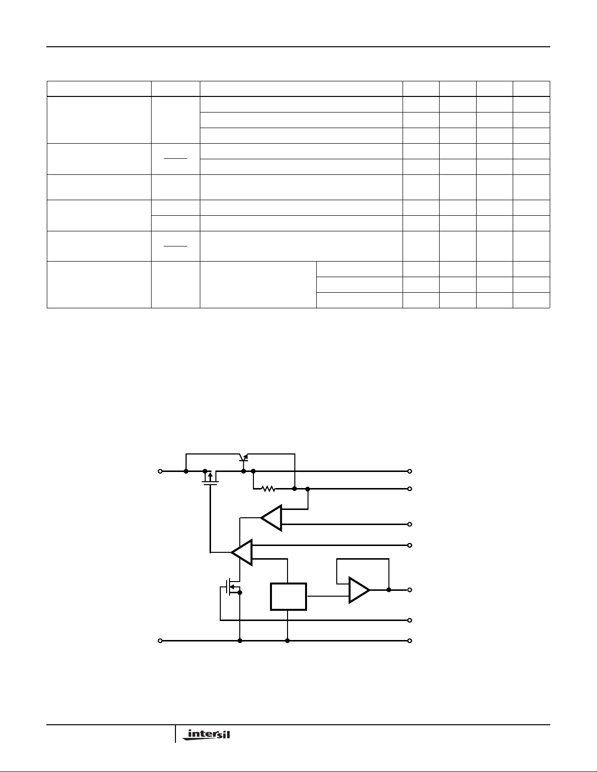
Functional Diagram
V+
GND
8
IN
C
A
REF
B
3
V
2
V
1
SENSE
6
V
7
V
5
SHUTDOWN
4
GND
OUT1
OUT2
SET
TC
3-57
 Loading...