

Intersil Corporation ICL7660, ICL7660A Datasheet

3-26
File Number
3072.4
ICL7660, ICL7660A
CMOS Voltage Converters
The Intersil ICL7660 and ICL7660A are monolithic CMOS
power supply circuits which offer unique performance
advantages over previously available devices. The ICL7660
performs supply voltage conversions from positive to
negative for an input range of +1.5V to +10.0V resulting in
complementary output voltages of -1.5V to -10.0V and the
ICL7660A does the same conversionswithaninputrangeof
+1.5V to +12.0V resulting in complementary output voltages
of -1.5V to -12.0V. Only 2 noncritical external capacitors are
needed for the charge pump and charge reservoir functions.
The ICL7660 and ICL7660A can also be connected to
function as voltage doublers and will generate output
voltages up to +18.6V with a +10V input.
Contained on the chip are a series DC supply regulator, RC
oscillator, voltage level translator, and four output power
MOS switches. A unique logic element senses the most
negative voltage in the deviceand ensures that the output NChannel switch source-substrate junctions are not forward
biased. This assures latchup free operation.
The oscillator, when unloaded, oscillates at a nominal
frequency of 10kHz for an input supply voltage of 5.0V. This
frequency can be lowered by the addition of an external
capacitor to the “OSC” terminal, or the oscillator may be
overdriven by an external clock.
The “LV” terminal may be tied to GROUND to bypass the
internal series regulator and improve low voltage (LV)
operation. At medium to high voltages (+3.5V to +10.0V for
the ICL7660 and +3.5V to +12.0V for the ICL7660A), the LV
pin is left floating to prevent device latchup.
Features
• Simple Conversion of +5V Logic Supply to ±5V Supplies
• Simple Voltage Multiplication (V
OUT
= (-) nVIN)
• Typical Open Circuit Voltage Conversion Efficiency 99.9%
• Typical Power Efficiency 98%
• Wide Operating Voltage Range
- ICL7660 . . . . . . . . . . . . . . . . . . . . . . . . . .1.5V to 10.0V
- ICL7660A . . . . . . . . . . . . . . . . . . . . . . . . .1.5V to 12.0V
• ICL7660A 100% Tested at 3V
• Easy to Use - Requires Only 2 External Non-Critical
Passive Components
• No External Diode Over Full Temp. and Voltage Range
Applications
• On Board Negative Supply for Dynamic RAMs
• Localized µProcessor (8080 Type) Negative Supplies
• Inexpensive Negative Supplies
• Data Acquisition Systems
Pinouts
ICL7660, ICL7660A (PDIP, SOIC)
TOP VIEW
ICL7660 (METAL CAN)
TOP VIEW
Ordering Information
PART NO.
TEMP.
RANGE (oC) PACKAGE
PKG.
NO.
ICL7660CBA 0 to 70 8 Ld SOIC (N) M8.15
ICL7660CBA-T 0 to 70 8 Ld SOIC (N)
Tape and Reel
M8.15
ICL7660CPA 0 to 70 8 Ld PDIP E8.3
ICL7660MTV† 0 to 70 8 Pin Metal Can T8.C
ICL7660ACBA 0 to 70 8 Ld SOIC (N) M8.15
ICL7660ACBA-T 0 to 70 8 Ld SOIC (N)
Tape and Reel
M8.15
ICL7660ACPA 0 to 70 8 Ld PDIP E8.3
ICL7660AIBA -40 to 85 8 Ld SOIC (N) M8.15
ICL7660AIBA-T -40 to 85 8 Ld SOIC (N)
Tape and Reel
M8.15
ICL7660AIPA -40 to 85 8 Ld PDIP E8.3
† Add /883B to part number if 883B processing is required.
NC
CAP+
GND
CAP-
1
2
3
4
8
7
6
5
V+
OSC
LV
V
OUT
V+ (AND CASE)
LV
CAP+
NC
GND
OSC
V
OUT
2
4
6
1
3
7
5
8
CAP-
Data Sheet April 1999
CAUTION: These devices are sensitive to electrostatic discharge; follow proper IC Handling Procedures.
http://www.intersil.com or 407-727-9207
| Copyright © Intersil Corporation 1999
3-27
C
Absolute Maximum Ratings Thermal Information
Supply Voltage
ICL7660 . . . . . . . . . . . . . . . . . . . . . . . . . . . . . . . . . . . . . . . +10.5V
ICL7660A . . . . . . . . . . . . . . . . . . . . . . . . . . . . . . . . . . . . . . +13.0V
LV and OSC Input Voltage. . . . . . -0.3V to (V+ +0.3V) for V+ < 5.5V
(Note 2) . . . . . . . . . . . . . . (V+ -5.5V) to (V+ +0.3V) for V+ > 5.5V
Current into LV (Note 2). . . . . . . . . . . . . . . . . . . 20µA for V+ > 3.5V
Output Short Duration (V
SUPPLY
≤ 5.5V) . . . . . . . . . . . .Continuous
Operating Conditions
Temperature Range
ICL7660M. . . . . . . . . . . . . . . . . . . . . . . . . . . . . . . -55oC to 125oC
ICL7660C, ICL7660AC. . . . . . . . . . . . . . . . . . . . . . . .0oC to 70oC
ICL7660AI . . . . . . . . . . . . . . . . . . . . . . . . . . . . . . . -40oC to 85oC
Thermal Resistance (Typical, Note 1) θJA (oC/W) θJC (oC/W)
PDIP Package . . . . . . . . . . . . . . . . . . . 150 N/A
SOIC Package . . . . . . . . . . . . . . . . . . . 165 N/A
Metal Can Package (ICL7660 Only). . . 160 70
Maximum Storage Temperature Range. . . . . . . . . . -65oC to 150oC
Maximum Lead Temperature (Soldering, 10s). . . . . . . . . . . . .300oC
(SOIC - Lead Tips Only)
CAUTION: Stresses above those listed in “Absolute Maximum Ratings” may cause permanent damage to the device. This is a stress only rating and operationofthe
device at these or any other conditions above those indicated in the operational sections of this specification is not implied.
NOTE:
1. θJA is measured with the component mounted on an evaluation PC board in free air.
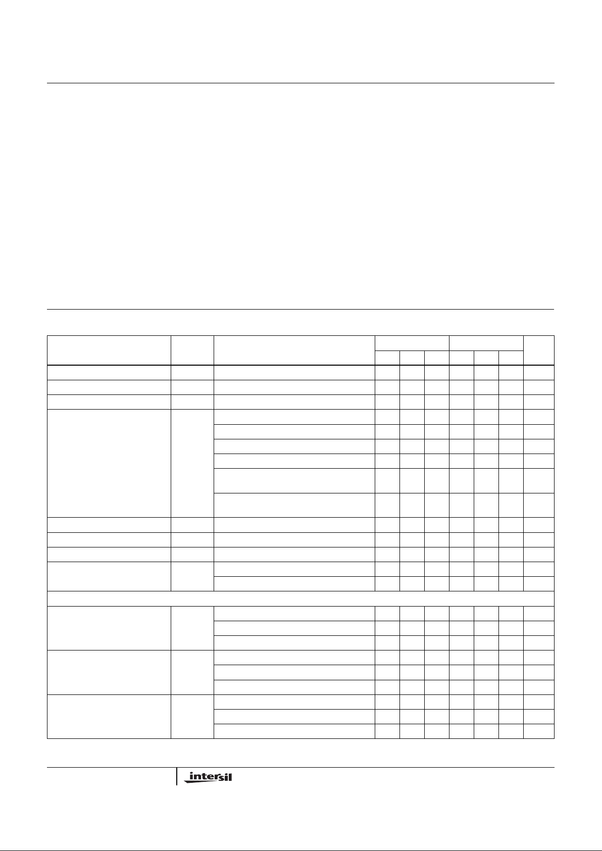
Electrical Specifications ICL7660 and ICL7660A, V+ = 5V, T
A
= 25oC, C
OSC
= 0, Test Circuit Figure 11
Unless Otherwise Specified
PARAMETER SYMBOL TEST CONDITIONS
ICL7660 ICL7660A
UNITSMIN TYP MAX MIN TYP MAX
Supply Current I+ R
L
= ∞ - 170 500 - 80 165 µA
Supply Voltage Range - Lo VL+ MIN ≤ TA≤ MAX, RL = 10kΩ, LV to GND 1.5 - 3.5 1.5 - 3.5 V
Supply Voltage Range - Hi VH+ MIN ≤ TA≤ MAX, RL = 10kΩ, LV to Open 3.0 - 10.0 3 - 12 V
Output Source Resistance R
OUTIOUT
= 20mA, TA = 25oC - 55 100 - 60 100 Ω
I
OUT
= 20mA, 0oC ≤ TA≤ 70oC - - 120 - - 120 Ω
I
OUT
= 20mA, -55oC ≤ TA≤ 125oC - - 150 - - - Ω
I
OUT
= 20mA, -40oC ≤ TA≤ 85oC -----120Ω
V
+
= 2V, I
OUT
= 3mA, LV to GND
0oC ≤ TA≤ 70oC
- - 300 - - 300 Ω
V+ = 2V, I
OUT
= 3mA, LV to GND,
-55oC ≤ TA≤ 125oC
--400---Ω
Oscillator Frequency f
OSC
-10- -10-kHz
Power Efficiency P
EF
RL = 5kΩ 95 98 - 96 98 - %
Voltage Conversion Efficiency V
OUT EFRL
= ∞ 97 99.9 - 99 99.9 - %
Oscillator Impedance Z
OSC
V+ = 2V - 1.0 - - 1 - MΩ
V = 5V -100----kΩ
ICL7660A, V+ = 3V, TA = 25oC, OSC = Free running, Test Circuit Figure 11, Unless Otherwise Specified
Supply Current (Note 3) I+ V+ = 3V, RL = ∞, 25oC - - - - 26 100 µA
0oC < TA<70oC -----125µA
-40oC < TA < 85oC -----125µA
Output Source Resistance R
OUT
V+ = 3V, I
OUT
= 10mA - - - - 97 150 Ω
0oC < TA<70oC -----200Ω
-40oC < TA <85oC -----200Ω
Oscillator Frequency (Note 3) f
OSC
V+ = 3V (same as 5V conditions) - - - 5.0 8 - kHz
0oC < TA<70oC - - - 3.0 - - kHz
-40oC < TA <85oC - - - 3.0 - - kHz
ICL7660, ICL7660A

3-28
Functional Block Diagram
Voltage Conversion Efficiency V
OUT
EFF V+ = 3V, RL = ∞ ---99--%
T
MIN
< TA < T
MAX
---99--%
Power Efficiency P
EFF
V+ = 3V, RL = 5kΩ ---96--%
T
MIN
< TA < T
MAX
---95--%
NOTES:
2. Connecting any input terminal tovoltagesgreaterthan V+ or less than GND may cause destructive latchup. Itisrecommended that no inputs
from sources operating from external supplies be applied prior to “power up” of the ICL7660, ICL7660A.
3. Derate linearly above 50oC by 5.5mW/oC.
4. In the test circuit,thereis no external capacitor applied to pin7.However, when the device is plugged intoatest socket, there is usually a very
small but finite stray capacitance present, of the order of 5pF.
5. The Intersil ICL7660A can operatewithoutan external diode over the full temperature and voltage range. This device will function in existing
designs which incorporate an external diode with no degradation in overall circuit performance.
Electrical Specifications ICL7660 and ICL7660A, V+ = 5V, T
A
= 25oC, C
OSC
= 0, Test Circuit Figure 11
Unless Otherwise Specified (Continued)
PARAMETER SYMBOL TEST CONDITIONS
ICL7660 ICL7660A
UNITSMIN TYP MAX MIN TYP MAX
RC
OSCILLATOR
÷2
VOLTAGE
LEVEL
TRANSLATOR
VOLTAGE
REGULATOR
LOGIC
NETWORK
OSC LV
V+
CAP+
CAP-
V
OUT
Typical Performance Curves
(Test Circuit of Figure 11)
FIGURE 1. OPERATING VOLTAGE AS A FUNCTION OF
TEMPERATURE
FIGURE 2. OUTPUT SOURCE RESISTANCE AS A FUNCTION
OF SUPPLY VOLTAGE
10
SUPPLY VOLTAGE RANGE
(NO DIODE REQUIRED)
8
6
4
2
0
-55 -25 0 25 50 100 125
TEMPERATURE (
o
C)
SUPPLY VOLTAGE (V)
10K
TA = 25oC
1000
100
10
01 2345678
SUPPLY VOLTAGE (V+)
OUTPUT SOURCE RESISTANCE (Ω)
ICL7660, ICL7660A
 Loading...