Intersil Corporation ICL7149, ICL7139 Datasheet

August 1997
ICL7139, ICL7149
33/4 Digit,
Autoranging Multimeter
Features
• 13 Ranges - ICL7139
- 4 DC Voltage 400mV, 4V, 40V, 400V
- 1 AC Voltage 400V
- 4 DC Current 4mA, 40mA, 400mA, 4A
- 4 Resistance 4kΩ, 40kΩ, 400kΩ, 4MΩ
• 18 Ranges - ICL7149
- 4 DC Voltage 400mV, 4V, 40V, 400V
- 2 AC Voltage with Optional AC Circuit
- 4 DC Current 4mA, 40mA, 400mA, 4A
- 4 AC Current with Optional AC Circuit
- 4 Resistance 4kΩ, 40kΩ, 400kΩ, 4MΩ
• Autoranging - First Reading is Always on Correct Range
• On-Chip Duplex LCD Display Drive Including Three Decimal Points and 11 Annunciators
• No Additional Active Components Required
• Low Power Dissipation - Less than 20mW - 1000 Hour
Typical Battery Life
• Display Hold Input
• Continuity Output Drives Piezoelectric Beeper
• Low Battery Annunciator with On-Chip Detection
• Guaranteed Zero Reading for 0V Input on All Ranges
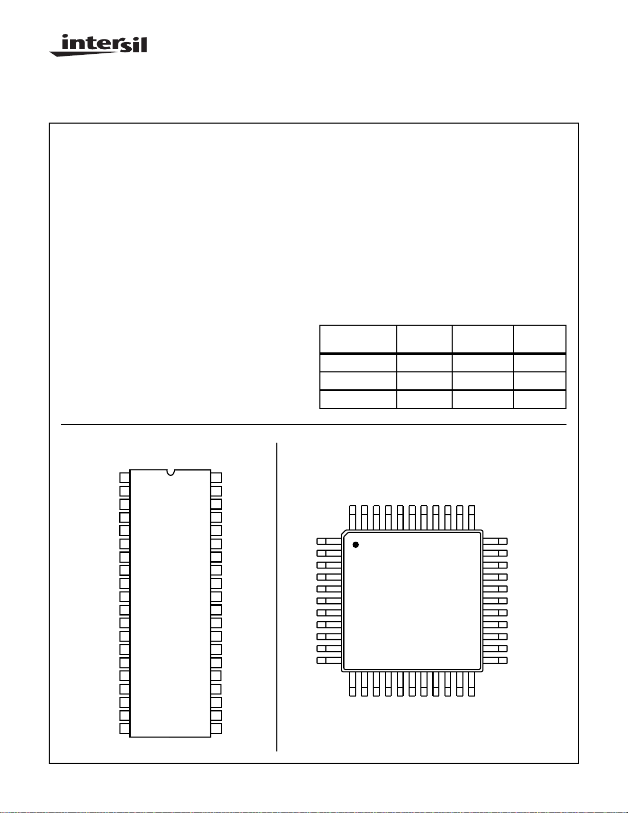
Pinouts
ICL7139, ICL7149 (PDIP)
TOP VIEW
Description
The Intersil ICL7139 and ICL7149 are high performance, low
power, auto-ranging digital multimeter lCs. Unlike other
autoranging multimeter ICs, the ICL7139 and ICL7149
always display the result of a conversion on the correct
range. There is no “range hunting” noticeable in the display.
The unit will autorange between the four different ranges. A
manual switch is used to select the 2 high group ranges. DC
current ranges are 4mA and 40mA in the low current group,
and 400mA and 4A in the high current group. Resistance
measurements are made on 4 ranges, which are divided into
two groups. The low resistance ranges are 4/40kΩ. The high
resistance ranges are 0.4/4MΩ. Resolution on the lowest
range is 1Ω.
Ordering Information
TEMP.
PART NUMBER
ICL7139CPL 0 to 70 40 Ld PDIP E40.6
ICL7149CPL 0 to 70 40 Ld PDIP E40.6
ICL7149CM44 0 to 70 44 Ld MQFP Q44.10x10
RANGE (oC) PACKAGE PKG. NO.
ICL7149 (MQFP)
TOP VIEW
BP2
BP1
V+
V
REF
LOΩ
HIΩ
DEINT
INT 1
C
AZ
C
INT
V/Ω/A
HOLD
1
2
3
4
V-
5
6
7
8
9
10
11
12
13
14
15
16
17
18
19
20
40
39
38
37
36
35
34
33
32
31
30
29
28
27
26
25
24
23
22
21
ADG
3/E3
B3/C
3
F2/DP
3
G2/E
2
A2/D
2
B2/C
2
F1/DP
2
G1/E
1
A1/D
1
B1/C
1
F0/DP
1
G0/E
0
A0/D
0
B0/C
0
LO BAT/V
MΩ/µA
Ω/A
k/m
OSC IN
OSC OUT
A2/D
G2/E
F2/DP
B3/C
ADG
3/E3
POL/AC
NC
BP2
BP1
V+
NC
2
2
/C
/DP
2
1
B
F
44 43 42 41 40
2
2
3
3
1
2
3
4
5
6
7
8
9
10
11
12 13 14 15 16 17
V-
REF
V
| Copyright © Intersil Corporation 1999
POL/AC
COMMON
INT V/Ω
TRIPLE POINT
BEEPER OUT
mA/µA
IΩ-DC/LOΩ-AC
CAUTION: These devices are sensitive to electrostatic discharge; follow proper IC Handling Procedures.
http://www.intersil.com or 407-727-9207
3-33
1
1
1
/E
/D
/C
1
1
1
G
A
B
HIΩ
LOΩ
DEINT
1
0
0
0
/E
/D
0
G
INT 1
0
A
INT V/Ω
/C
0
B
NC
2221201918
AZ
C
TRIPLE POINT
/DP
0
F
39 38 37 36 35 34
COMMON
LO BAT/V
33
32
31
30
29
28
27
26
25
24
23
INT
C
MΩ/µA
Ω/A
k/m
OSC IN
OSC OUT
HOLD
HIΩ-DC/LOΩ-AC
V/Ω/A
mA/µA
BEEPER OUT
NC
File Number 3088.1

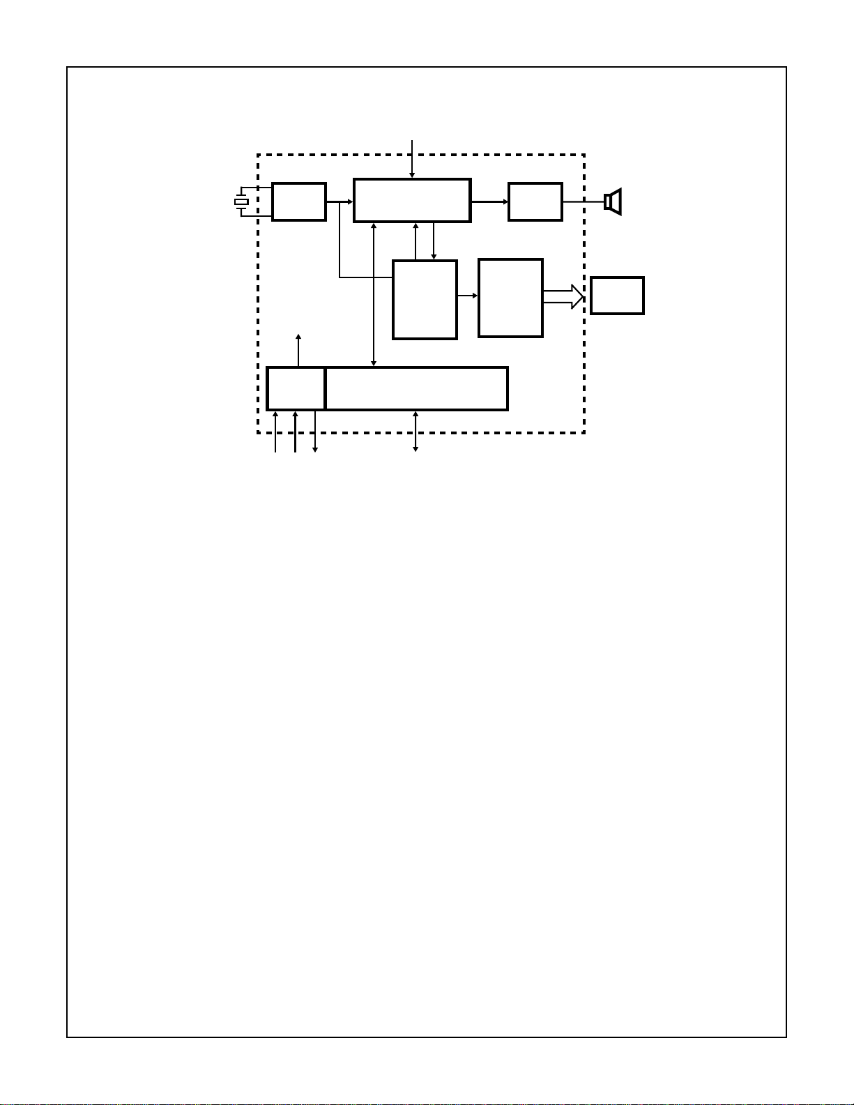
Functional Block Diagram
ICL7139, ICL7149
SWITCHES
CRYSTAL
OSC
DIGITAL COMMON
POWER
SUPPLY
SECTION
V+ V- COM
ANALOG SWITCHES, INTEGRATION
CONTROL LOGIC
INCLUDING
AUTORANGING LOGIC
COUNTERS
ANALOG SECTION
AND COMPARATOR
EXTERNAL
RESISTORS
AND CAPACITORS
BEEPER
DRIVER
DISPLAY
DRIVER
AND
LATCHES
PIEZO
ELECTRIC
BEEPER
DISPLAY
3-34

ICL7139, ICL7149
Absolute Maximum Ratings Thermal Information
Supply Voltage (V+ to V-) . . . . . . . . . . . . . . . . . . . . . . . . . . . . . . 15V
Reference Input Voltage (V
Analog Input Current (IN + Current or IN + Voltage) . . . . . . . 100µA
Clock Input Swing. . . . . . . . . . . . . . . . . . . . . . . . . . . . . . V+ to V+ -3
to COM) . . . . . . . . . . . . . . . . . . . 3V
REF
Operating Conditions
Temperature Range . . . . . . . . . . . . . . . . . . . . . . . . . . . .0oC to 70oC
CAUTION: Stresses above those listed in “Absolute Maximum Ratings” may cause permanent damage to the device. This is a stress only rating and operation
of the device at these or any other conditions above those indicated in the operational sections of this specification is not implied.
NOTE:
1. θJA is measured with the component mounted on an evaluation PC board in free air.
Thermal Resistance (Typical, Note 1) θJA (oC/W)
PDIP Package. . . . . . . . . . . . . . . . . . . . . . . . . . . . . . . 50
MQFP Package. . . . . . . . . . . . . . . . . . . . . . . . . . . . . . 80
Maximum Junction Temperature . . . . . . . . . . . . . . . . . . . . . . . 150oC
Maximum Storage Temperature Range . . . . . . . . . .-65oC to 150oC
Maximum Lead Temperature (Soldering 10s) . . . . . . . . . . . . . 300oC
(MQFP - Lead Tips Only)
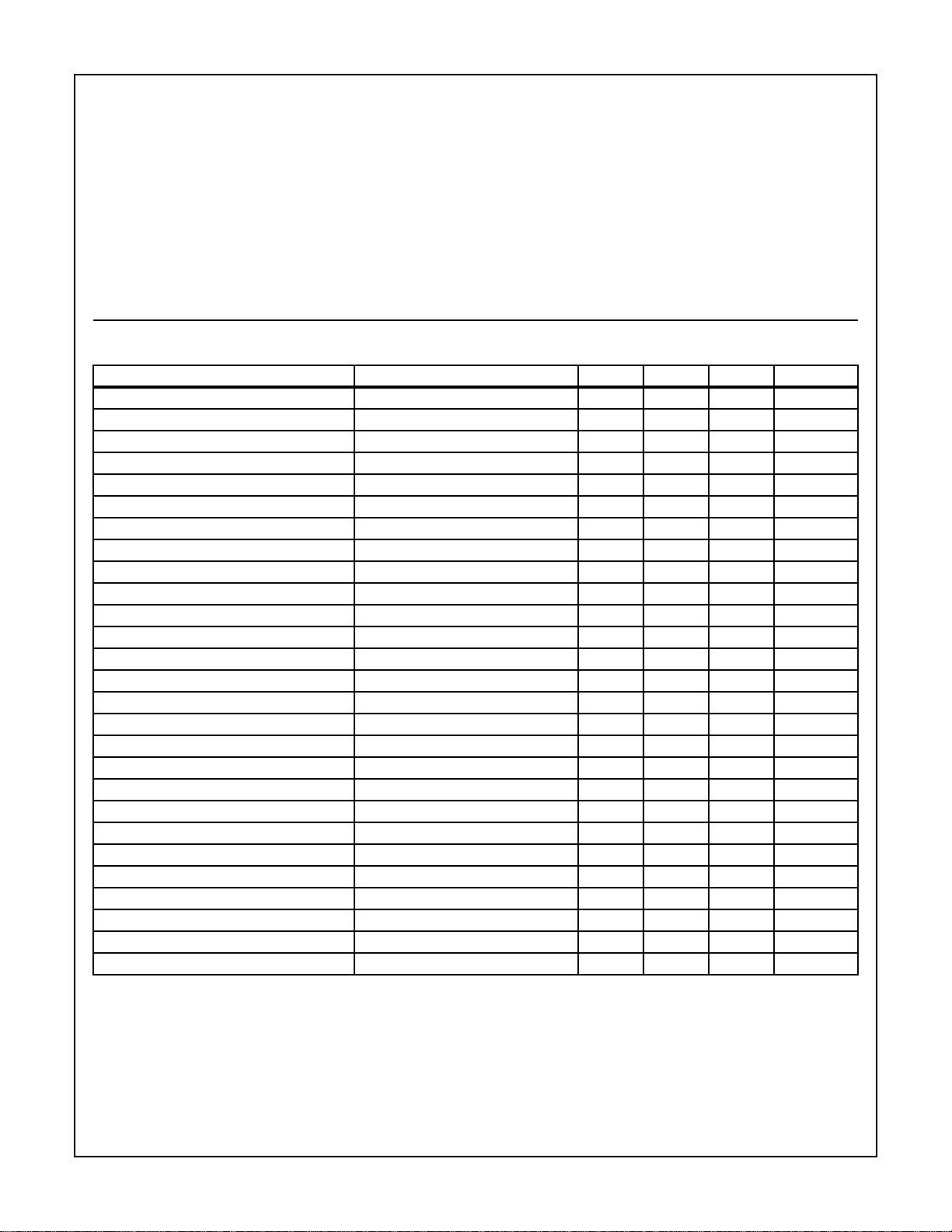
Electrical Specifications V+ = 9V, T
Crystal = 120kHz. (See Figure 14)
PARAMETER TEST CONDITIONS MIN TYP MAX UNITS
Zero Input Reading VIN or IIN or RIN = 0.00 -00.0 - +00.0 V, I, Ω
Linearity (Best Straight Line) (Note 6) (Notes 1 and 8) -1
Accuracy DC V, 400V Range Only (Notes 1 and 8) - - ±1 % of RDG ±1
Accuracy DC V, 400V Range Excluded (Notes 1 and 8) - - ±0.30 % of RDG ±1
Accuracy Ω, 4K and 400K Range (Notes 1 and 8) - - ±0.75 % of RDG ±8
Accuracy Ω, 4K and 4M Range (Notes 1 and 8) - - ±1 % of RDG ±9
Accuracy DC I, Unadjusted for Full Scale (Notes 1 and 8) - - ±0.75 % of RDG ±1
Accuracy DC I, Adjusted for Full Scale (Notes 1 and 8) - ±0.2 - % of RDG ±1
Accuracy AC V At 60Hz (Notes 5, 7, and 8) - ±2 - % of RDG
Open Circuit Voltage for Ω Measurements R
Noise VIN = 0, DC V (Note 2, 95% of Time) - 0.1 - LSB
Noise VIN = 0, AC V (Note 2, 95% of Time) - 4 - LSB
Supply Current VIN = 0, DC Voltage Range - 1.5 2.4 mA
Analog Common (with Respect to V+) I
Temperature Coefficient of Analog Common I
Output Impedance of Analog Common I
Backplane/Segment Drive Voltage Average DC < 50mV 2.8 3.0 3.2 V
Backplane/Segment Display Frequency - 75 - Hz
Switch Input Current VIN = V+ to V- (Note 3) -50 - +50 µA
Switch Input Levels (High Trip Point) V+ - 0.5 - V+ V
Switch Input Levels (Mid Trip Point) V- + 3 - V+ - 2.5 V
Switch Input Levels (Low Trip Point) V- - V- + 0.5 V
Beeper Output Drive (Rise or Fall Time) C
Beeper Output Frequency - 2 - kHz
Continuity Detect Range = Low Ω, V
Power Supply Functional Operation V+ to V- 7 9 11 V
Low Battery Detect V+ to V- (Note 4) 6.5 7 7.5 V
NOTES:
1. Accuracy is defined as the worst case deviation from ideal input value including: offset, linearity, and rollover error.
2. Noise is defined as the width of the uncertainty window (where the display will flicker) between two adjacent codes.
3. Applies to pins 17-20.
4. Analog Common falls out of regulation when the Low Battery Detect is asserted, however the ICL7139 and ICL7149 will continue to
operate correctly with a supply voltage above 7V and below 11V.
5. For 50Hz use a 100kHz crystal.
6. Guaranteed by design, not tested.
7. ICL7139 only.
8. RDG = Reading.
= 25oC, V
A
UNKNOWN
COMMON
COMMON
COMMON
LOAD
adjusted for -3.700 reading on DC volts, test circuit as shown in Figure 3.
REF
-
= Infinity - V
< 10µA 2.7 2.9 3.1 V
< 10µA, Temp. = 0oC T o 70oC - -100 - ppm/oC
< 10µA-110Ω
= 10nF - 25 100 µs
= 1.00V - 1.5 - kΩ
REF
REF
+1 Counts
-V
3-35

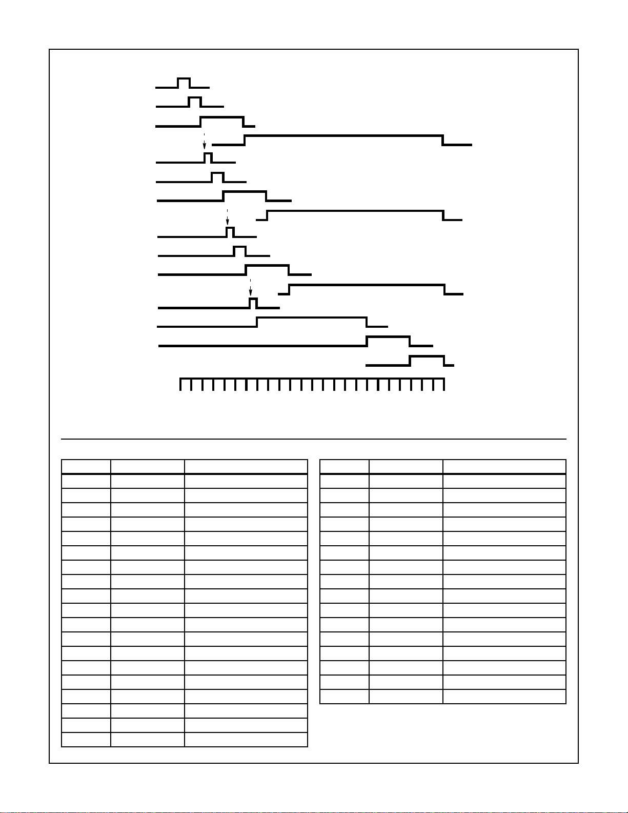
Timing Waveform
UNDERRANGE
UNDERRANGE
UNDERRANGE
ICL7139, ICL7149
FIRST AUTO ZERO
FIRST INTEGRATE
FIRST DEINTEGRATE
AUTO ZERO
SECOND AUTO ZERO
SECOND INTEGRATE
SECOND DEINTEGRATE
AUTO ZERO
THIRD AUTO ZERO
THIRD INTEGRATE
THIRD DEINTEGRATE
AUTO ZERO
FOURTH AUTO ZERO
FOURTH INTEGRATE
FOURTH DEINTEGRATE
AUTO ZERO
0123456789101112131415161718192021222324
FIGURE 1. LINE FREQUENCY CYCLES (1 CYCLE = 1000 INTERNAL CLOCK PULSES = 2000 OSCILLATION CYCLES)
Pin Descriptions
I/O PIN NUMBER DESCRIPTION
O 1 Segment Driver POL/AC
O 2 Backplane 2
O 3 Backplane 1
I4V+
I5V-
I 6 Reference Input
O7LoΩ
O8HiΩ
I/O 9 Deintegrate
I/O 10 Analog Common
I 11 Int I
I 12 Int V/Ω
I 13 Triple Point
I 14 Auto Zero Capacitor (CAZ)
I 15 Integrate Capacitor (C
O 16 Beeper Output
I17mA/µA
I18Ω/V/A
I19HiΩ DC/LoΩ AC
INT
)
I/O PIN NUMBER DESCRIPTION
I 20 Hold
O 21 Oscillator Out
I 22 Oscillator In
O 23 Segment DRIVER k/m
O 24 Segment Driver Ω/A
O 25 Segment Driver M Ω/µA
O 26 Segment Driver Lo Bat/V
O 27 Segment Driver B0/C
O 28 Segment Driver A0/D
O 29 Segment Driver G0/E
O 32 Segment Driver A1/D
O 33 Segment Driver G1/E
O 34 Segment Driver F1/DP
O 35 Segment Driver B2/C
O 39 Segment Driver B3/C
O 40 Segment Driver ADG3/E
NOTE: For segment drivers, segments are listed as (segment for
backplane 1)/(segment for backplane 2). Example: pin 27; segment
B0 is on backplane 1, segment C0 is on backplane 2.
0
0
0
1
1
1
1
3
3
3-36
 Loading...