intersil ICL7134 DATA SHEET
查询ICL7134供应商
December 1997
®
D
W
E
N
R
O
F
D
E
D
N
E
M
M
O
C
E
R
T
O
N
S
N
G
I
S
E
ICL7134
14-Bit Multiplying
Microprocessor-Compatible D/A Converter
Features
• 14-Bit Linearity (0.003% FSR)
• No Gain Adjustment Necessary
• Microprocessor-Compatible with Double Buffered
Inputs
• Bipolar Application Requires No Extra Adjustments or
External Resistors
• Low Linearity and Gain Temperature Coefficients
• Low Power Dissipation
• Full Four-Quadrant Multiplication
• 883B Processed Versions Available
Description
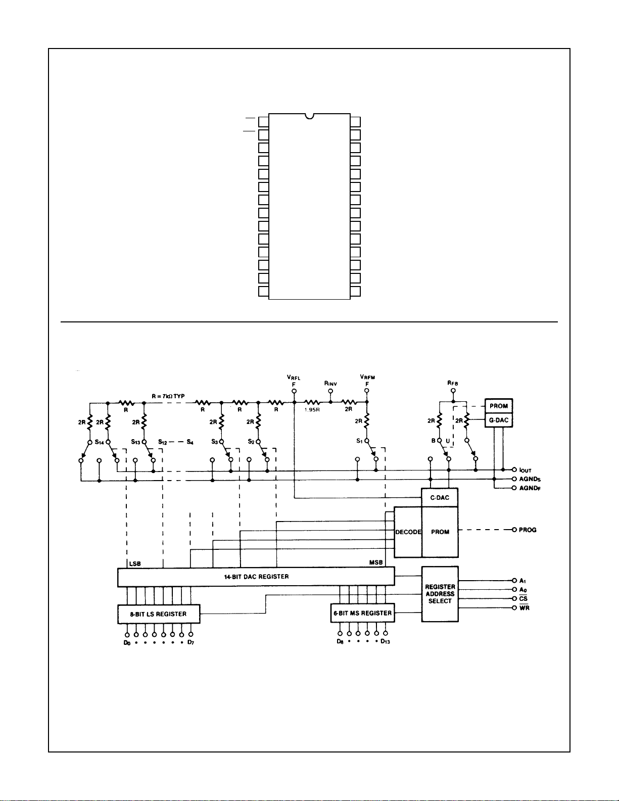
The ICL7134 combines a four-quadrant multiplying DAC
using thin film resistor and CMOS circuitry with an on-chip
PROM-controlled correction circuit to achieve true 14-bit
linearity without laser trimming.
Microprocessor bus interfacing is eased using standard
memory WRITE cycle timing and control signal use. Two
input buffer registers are separately loaded with the 8 least
significant bits (LS register) and the 6 most significant bits
(MS register). Their contents are then transferred to the
14-bit DAC register, which controls the current switches. The
DAC register can also be loaded directly from the data
inputs, in which case the MS and LS registers are
transparent.
The ICL7134 is available in two versions. The ICL7134U is
programmed for unipolar operation while the ICL7134B is
programmed for bipolar applications. The V
most significant bit of the DAC is separated from the
reference input to the remainder of the ladder. For unipolar
use, the two reference inputs are tied together, while for
bipolar operation, the polarity of the MSB reference is
reversed, giving the DAC a true 2’s complement input
transfer function. Two resistors which facilitate the reference
inversion are included on the chip, so only an external
op-amp is needed. The PROM is coded to correct for errors
in these resistors as well as the inversion of the MSB.
input to the
REF
Ordering Information
TEMPERATURE RANGE (oC)
NON-LINEARITY AT 25oC
BIPOLAR VERSIONS
0.01% (12-bit) ICL7134BJCJI ICL7134BJIJI ICL7134BJMJI 28 Ld CERDIP
0.006% (13-bit) ICL7134BKCJI ICL7134BKIJI ICL7134BKMJI 28 Ld CERDIP
0.003% (14-bit) ICL7134BLCJI ICL7134BLIJI ICL7134BLMJI 28 Ld CERDIP
UNIPLAR VERSIONS
0.01% (12-bit) ICL7134UJCJI ICL7134UJIJI ICL7134UJMJI 28 Ld CERDIP
0.006% (13-bit) ICL7134UKCJI ICL7134UKIJI ICL7134UKMJI 28 Ld CERDIP
0.003% (14-bit) ICL7134ULCJI ICL7134ULIJI ICL7134ULMJI 28 Ld CERDIP
CAUTION: These devices are sensitive to electrostatic discharge; follow proper IC Handling Procedures.
1-888-INTERSIL or 321-724-7143
Copyright © Intersil Americas Inc. 2002. All Rights Reserved
| Intersil (and design) is a registered trademark of Intersil Americas Inc.
1
PACKAGE0 to 70 -25 to 85 -55 to 125
File Number 3113.1
Pinout
ICL7134
ICL7134
(OUTLINE DWG JI)
TOP VIEW
Functional Block Diagram
WR
(LSB) D
D
D
CS
D
D
D
D
D
D
D
D
D
1
2
3
0
4
1
5
2
6
3
7
4
8
5
9
6
10
7
11
8
12
9
13
10
14
11
28
27
26
25
24
23
22
21
20
19
18
17
16
15
A
0
A
1
V+
I
OUT
AGND
AGND
DGND
R
FB
V
RFM
R
INV
V
RFL
PROG
(MSB)
D
13
D
12
S
F
2
Pin Descriptions
ICL7134
28 LEAD
CERDIP
PIN
NAME PIN DESCRIPTION
1CS
2WR
3D
4D
5D
6D
7D
8D
9D
10 D
11 D
12 D
13 D
14 D
10
11
Chip Select (active low). Enables register write.
WRITE, (active low). Writes in register. Equivalent to CS.
0
1
2
3
4
5
6
7
8
9
Bit 0 Least Significant
Bit1
Bit 2
Bit 3
Bit 4
Bit 5
Bit 6
Bit 7
Bit 8
Bit 9
Bit 10
Bit 11
Input Data Bits (High = True)
15 D
16 D
12
13
Bit 12
Bit 13 Most significant
17 PROG Used for programming only. Tie to +5V for normal operation.
18 V
19 R
20 V
21 R
RFLVREF
INV
RFM
FB
for lower bits.
Summing node for reference inverting amplifier.
FV
for MSB only (bipolar)
REF
Feedback resistor for voltage output applications.
22 DGND Digital Ground Return.
23 AGND
24 AGND
25 I
Analog Ground force lines. Use to carry current from internal Analog GND connections. Tied internally to AGNDS.
F
Analog Ground sense line. Reference point for external circuitry. Pin should carry minimal current; tied internally to
S
AGND
.
F
Current output pin.
OUT
26 V+ Positive Supply.
27 A
28 A
Address 1 Registers Select Lines
1
Address 0
0
3
ICL7134
Absolute Maximum Ratings (Note 1) Thermal Information
Supply Voltage (V+ to DGND) . . . . . . . . . . . . . . . . . . . -0.3V to 7.5V
V
, V
, R
RFL
RFM
I
, AGNDF, AGNDS . . . . . . . . . . . . . . . . . . . . . . . . . -0.1V to V+
OUT
Current in AGND
An, Dn, WR
, RFB to DGND . . . . . . . . . . . . . . . . . . . . . . . . ±15V
INV
, AGNDF . . . . . . . . . . . . . . . . . . . . . . . . . . . 25mA
S
, CS, PROG. . . . . . . . . . . . . . . . . . . . -0.3V to V+ +0.3V
Storage Temperature Range . . . . . . . . . . . . . . . . . .-65
Power Dissipation (Note 2) . . . . . . . . . . . . . . . . . . . . . . . . . . 500mW
Derate Linearly Above 70
o
C @10mW/oC
Lead Temperature (Soldering, 10s) . . . . . . . . . . . . . . . . . . . . 300
Operating Conditions
Temperature Range
ICL7134XXC . . . . . . . . . . . . . . . . . . . . . . . . . . . . . . . .0
ICL7134XXI. . . . . . . . . . . . . . . . . . . . . . . . . . . . . . . -25
ICL7134XXM. . . . . . . . . . . . . . . . . . . . . . . . . . . . . -55
CAUTION: Stresses above those listed in “Absolute Maximum Ratings” may cause permanent damage to the device. This is a stress only rating and operation
of the device at these or any other conditions above those indicated in the operational sections of this specification is not implied.
NOTES:
1. All voltages with respect to DGND.
2. Assumes all leads soldered or welded to printed circuit board.
o
C to 70oC
o
C to 85oC
o
C to 125oC
o
C to 150oC
o
C
Electrical Specification V+ = +5V, V
= +10V, TA = 25oC, AGND = DGND, I
REF
at Ground Potential,
OUT
Unless Otherwise Specified.
PARAMETER TEST CONDITIONS MIN TYP MAX UNITS
DC ACCURACY
Resolution 14 - - Bits
Non-Linearity (Notes 3 and 4) Figure 2 J - - ±0.012 %FSR
K- -±0.006 %FSR
L- -±0.003 %FSR
Non-Linearity Temperature
Operating Temperature Range (Note 5) - ±1 ±2 ppm/
Coefficient
Monotonicity (Note 5) J 12 - - Bits
K13 - - Bits
L14 - - Bits
Gain Error (Notes 3 and 4)
Figure 1
J- -±0.024 %FSR
K- -±0.012 %FSR
L- -±0.006 %FSR
Gain Error Temperature
(Note 5) - ±2 ±8 ppm/
Coefficient
Output Leakage Current
(I
Terminal)
OUT
= 25oC--±10 nA
T
A
Operating Temperature Range - ±60 - nA
o
C
o
C
Long Term Stability of I
OUT
1000 Hours, 125oC, (Note 5) - ±10 - ppm/month
AC ACCURACY
Power Supply Rejection ∆V+ = ±10%, Figure 2, T
= 25oC-±10 ±100 ppm/V
A
Operating Temperature Range - - ±150 ppm/V
Feedthrough Error V
REF
= 20V
, 2kHz U - 250 - µV
P-P
Sinewave, Figure 3 B - 500 - µV
Output Current Setting Time To 1/2 LSB, Figure 4 - 1 - µs
Output Noise Equivalent to Johnson Noise of 7kΩ Resistor, Typical
4
P-P
P-P
ICL7134
Electrical Specification V+ = +5V, V
= +10V, TA = 25oC, AGND = DGND, I
REF
at Ground Potential,
OUT
Unless Otherwise Specified. (Continued)
PARAMETER TEST CONDITIONS MIN TYP MAX UNITS
REFERENCE INPUT
Input Resistance V
RFL
= V
RFM
, I
at Ground 4 7 10 kΩ
OUT
ANALOG OUTPUT
Output Capacitance
(I
Terminal)
OUT
DAC Register Outputs All LOW - 160 - pF
DAC Register Outputs All HIGH - 235 - pF
DIGITAL INPUTS
Low State Threshold Operating Temperature Range - - 0.8 V
High State Threshold 2.4 - - V
Input Current Inputs between DGND to V+ - - ±1 µA
Input Capacitance (Note 5) - 15 - pF
POWER SUPPLY
Supply Voltage Range Functional Operation, (Note 6) 3.5 - 6.0 V
Supply Current Excluding Ladder Network (Note 7) - 1.0 2.5 mA
NOTES:
3. Full-Scale Range (FSR) is 10V for unipolar mode, 20V (±10V) for bipolar mode.
4. Using internal feedback and reference inverting resistors.
5. Guaranteed by design, not production tested.
6. Gain error tested to 0.040% FSR, Specifications are not guaranteed.
7. D0 - D13 connected to 2.4V.
Switching Specifications V+ = 5V, T
PARAMETER SYMBOL TEST CONDITIONS MIN TYP MAX UNITS
Address-WRITE
Address-WRITE
CHIP SELECT
CHIP SELECT
Pulse Width Low t
WRITE
Data-WRITE
Data-WRITE
Set-Up Time t
Hold Time t
-WRITE Set-Up Time t
-WRITE Hold Time t
Set-Up Time t
Hold Time t
= 25oC, See Timing Diagram
A
AWs
AWh
CWs
CWh
WR
DWs
DWh
Note 5 0 - - ns
Note 5 0 - - ns
Note 5 0 - - ns
Note 5 0 - - ns
150 - - ns
200 - - ns
200 - - ns
5
 Loading...