Intersil Corporation ICL7129 Datasheet

August 1997
ICL7129
41/2Digit LCD,
Single-Chip A/D Converter
Features
• ±19,999 Count A/D Converter Accurate to ±4 Count
•10µV Resolution on 200mV Scale
• 110dB CMRR
• Direct LCD Display Drive
• True Differential Input and Reference
• Low Power Consumption
• Decimal Point Drive Outputs
• Overrange and Underrange Outputs
• Low Battery Detection and Indication
• 10:1 Range Change Input
Ordering Information
TEMP.
PART NUMBER
RANGE (oC) PACKAGE PKG. NO.
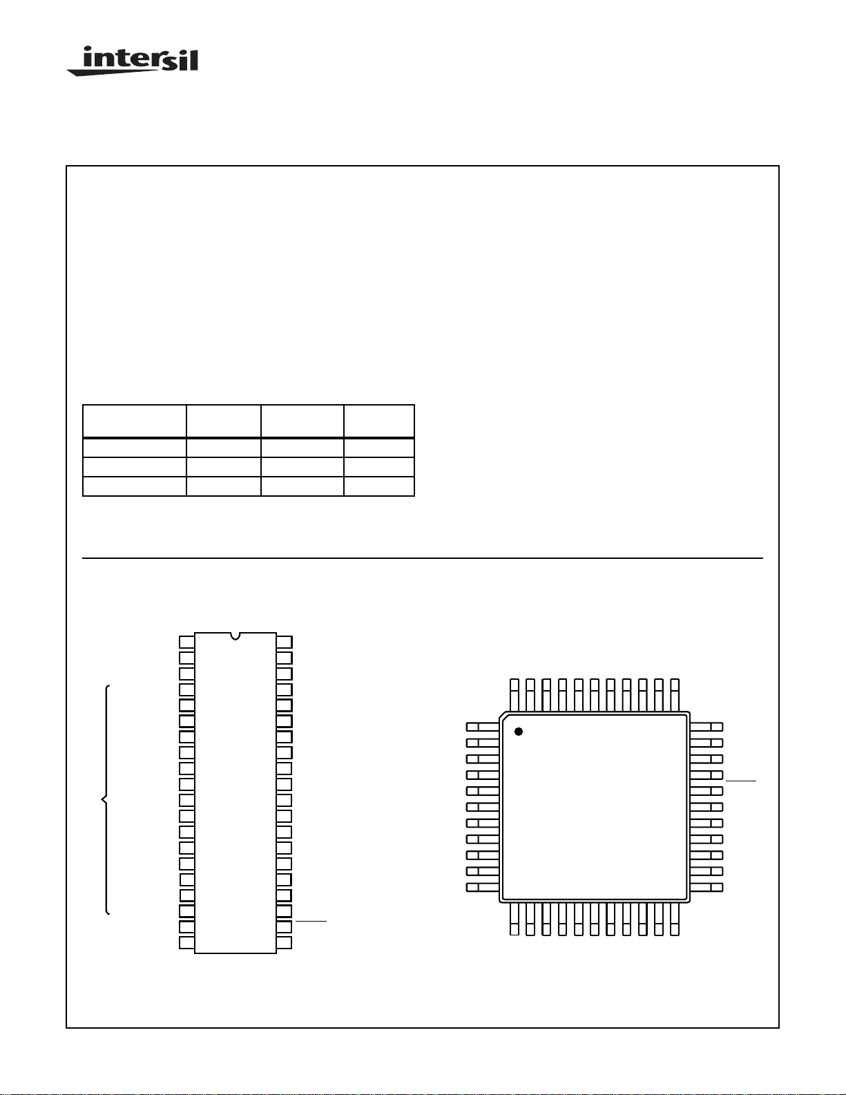
ICL7129CPL 0 to 70 40 Ld PDIP E40.6
ICL7129RCPL 0 to 70 40 Ld PDIP E40.6
ICL7129CM44 0 to 70 44 Ld MQFP Q44.10x10
NOTE: “R” indicates device with reversed leads.
Pinouts
ICL7129 (PDIP)
TOP VIEW
Description
The Intersil ICL7129 is a very high performance 41/2-digit,
analog-to-digital converter that directly drives a multiplexed
liquid crystal display. This single chip CMOS integrated circuit requires only a few passive components and a reference
to operate. It is ideal for high resolution hand-held digital
multimeter applications.
The performance of the ICL7129 has not been equaled
before in a single chip A/D converter. The successive integr ation technique used in the ICL7129 results in accuracy better
than 0.005% of full scale and resolution down to 10µV/count.
The ICL7129, drawing only 1mA from a 9V battery, is well
suited for battery powered instruments. Provision has been
made for the detection and indication of a “LOW/BATTERY”
condition. Autoranging instruments can be made with the
ICL7129 which provides overrange and underrange outputs
and 10:1 range changing input. The ICL7129 instantly checks
for continuity, giving both a visual indication and a logic level
output which can enable an external audible transducer. These
features and the high performance of the ICL7129 make it an
extremely versatile and accurate instrument-on-a-chip .
ICL7129 (MQFP)
TOP VIEW
OSC2
1
OSC1
2
ANNUNCIATOR
B2, C2, LO BAT
DISPLA Y OUTPUT LINES
CAUTION: These devices are sensitive to electrostatic discharge; follow proper IC Handling Procedures.
http://www.intersil.com or 407-727-9207
OSC3
DRIVE
B
, C1, CONT
1
A
, G1, D
1
F1, E1, DP
A
, G2, D
2
F2, E2, DP
B3, C3, MINUS
A
, G3, D
3
F3, E3, DP
B4, C4, BC
A4, D4, G
F4, E4, DP
BP3
BP2
BP1
V
DISP
DP4/OR
3
4
5
1
6
1
7
8
2
9
2
10
11
3
12
3
13
5
14
4
15
4
16
17
18
19
20
40
DP
39
1
DP
38
2
37
RANGE
36
DGND
35
REF LO
REF HI
34
IN HI
33
32
IN LO
31
BUFF
C
30
REF-
C
29
REF+
28
COMMON
27
CONTINUITY
26
INT OUT
25
INT IN
24
V+
23
V-
22
LATCH/HOLD
DP
21
3
/UR
B
| Copyright © Intersil Corporation 1999
DGND
RANGE
OSC 2
OSC 1
OSC 3
ANNUNCE
DRIVE
, C1, CONT
1
3-31
DP
DP
2
1
NC
NC
IN HI
IN LO
REF HI
REF LO
44 43 42 41 40
1
2
3
4
5
6
7
8
9
10
11
12 13 14 15 16 17
1
1
, DP
1
, E
1
F
, LO BA T
, C
B
2
, D
2
, G
2
2
A
2
, D
, G
A
1
1
+
-
REF
REF
BUFF
C
39 38 37 36 35 34
2
, DP
2
, MINUS
, E
3
2
F
, C
3
B
C
COMMON
3
, D
3
, DP
, G
, E
3
A
F
CONTINUITY
3
5
, BC
3
4
, C
3
4
B
File Number 3085.1
INT IN
INT OUT
33
32
31
30
29
28
27
26
25
24
23
2221201918
4
4
, G
4
, DP
4
, D
, E
4
4
A
F
V+
VNC
NC
LATCH/
HOLD
/UR
DP
3
DP4/OR
V
DISP
BP1
BP2
BP3

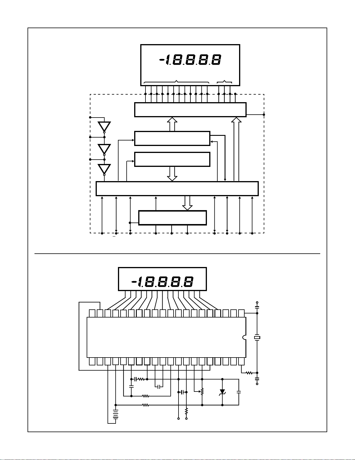
Functional Block Diagram
ICL7129
LOW BATTERY CONTINUITY
SEGMENT DRIVES
BACKPLANE
DRIVES
ANNUNCIATOR DRIVE
OSC1
OSC2
OSC3
Typical Application Schematic
LATCH, DECODE DISPLAY MULTIPLEXER
UP/DOWN RESULTS COUNTER
SEQUENCE COUNTER/DECODER
CONTROL LOGIC
ANALOG SECTION
DGNDV-V+CONTL/HRANGE
LOW BATTERY CONTINUITY
OR
DP
V
DISP
DP
DP
UR
DP
3
3
1
2
V+
5pF
13
14
15
16
17
18
19
20
10
11
12
7
8
9
4
5
6
1
2
3
ICL7129
28
27
26
25
24
23
22
21
31
30
29
34
33
32
37
36
35
40
39
38
(MICA)
120kHz
270K
560pF
(MICA)
1.2kΩ
150kΩ
10kΩ
+
1.0µF
20K
0.1µF
100kΩ
+
-
V
IN
ICL8069
6.8µF
0.1µF
+
9V
-
10pF
V+
3-32

ICL7129
Absolute Maximum Ratings Thermal Information
Supply Voltage . . . . . . . . . . . . . . . . . . . . . . . . . . . . . . . . . . . . . . 15V
Reference Voltage (REF HI or REF LO). . . . . . . . . . . . . . . . V+ to V-
Input Voltage (Note 1), IN HI or IN LO . . . . . . . . . . . . . . . . . V+ to V-
V
. . . . . . . . . . . . . . . . . . . . . . . . . . . . . . . . . .DGND -0.3V to V+
DISP
Digital Input Pins
1, 2, 19, 20, 21, 22, 27, 37, 38, 39, 40 . . . . . . . . . . . . .DGND to V+
CAUTION: Stresses above those listed in “Absolute Maximum Ratings” may cause permanent damage to the device. This is a stress only rating and operation
of the device at these or any other conditions above those indicated in the operational sections of this specification is not implied.
NOTES:
1. Input voltages may exceed the supply voltages pro vided that input current is limited to 1400mA. Currents abo ve this value may result in
valid display readings but will not destroy the device if limited to ±1mA.
2. θJA is measured with the component mounted on an evaluation PC board in free air.
Thermal Resistance (Typical, Note 2) θJA (oC/W)
PDIP Package. . . . . . . . . . . . . . . . . . . . . . . . . . . . . . . 50
MQFP Package. . . . . . . . . . . . . . . . . . . . . . . . . . . . . . 80
Maximum Junction Temperature . . . . . . . . . . . . . . . . . . . . . 150oC
Maximum Storage Temperature Range . . . . . . . . . .-65oC to 150oC
Maximum Lead Temperature (Soldering 10s) . . . . . . . . . . . . . 300oC
(MQFP - Lead Tips Only)
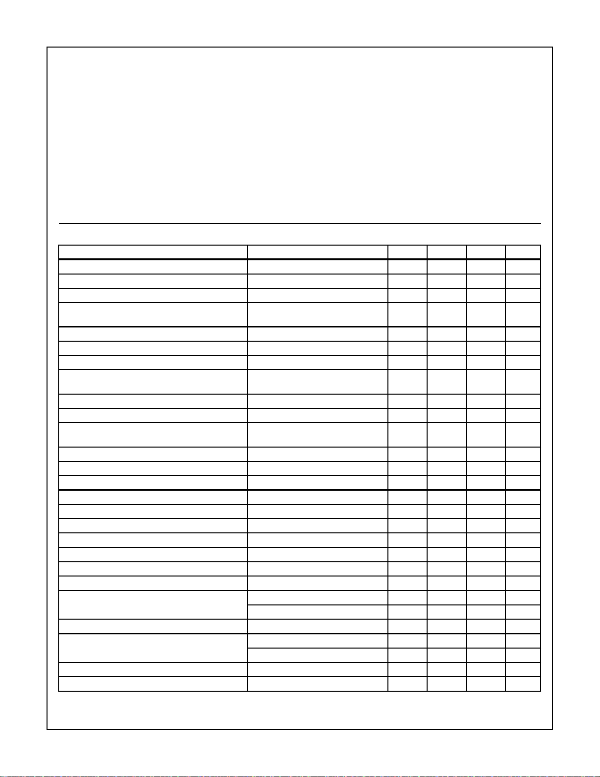
Electrical Specifications V- to V+ = 9V, V
= 1.00V, TA = 25oC, f
REF
= 120kHz, Unless Otherwise Specified
CLK
PARAMETER TEST CONDITIONS MIN TYP MAX UNITS
Zero Input Reading VIN = 0V, 200mV Scale -0000 0000 +0000 Counts
Zero Reading Drift V
Ratiometric Reading V
Range Change Accuracy V
= 0V, 0oC To 70oC-±0.5 - µV/oC
IN
= V
IN
IN
= 1000mV, RANGE = 2V 9996 9999 10000 Counts
REF
= 0.10000V on Low,
0.9999 1.0000 1.0001 Ratio
Range ≈ VIN = 1.0000V on High Range
Rollover Error -V
= +VIN = 199mV - 1.5 3.0 Counts
IN
Linearity Error 200mV Scale - 1.0 - Counts
Input Common-Mode Rejection Ratio V
Input Common-Mode Voltage Range V
= 1V,VIN = 0V, 200mV Scale - 110 - dB
CM
= 0V, 200mV Scale - (V-) +1.5
IN
-V
(V+) -1.0
Noise (Peak-To-Peak V alue not Exceeded 95% of Time) V
Input Leakage Current V
Scale Factor Tempco V
= 0V 200mV Scale - 14 - µV
IN
= 0V, Pin 32, 33 - 1 10 pA
IN
= 199mV 0oC To 70oC
IN
External V
= 0ppm/oC
REF
- 2 7 ppm/oC
COMMON Voltage V+ to Pin 28 2.8 3.2 3.5 V
COMMON Sink Current ∆Common = + 0.1V - 0.6 - mA
COMMON Source Current ∆Common = -0.1V - 10 - µA
DGND VoItage V+ to Pin 36, V+ to V- = 9V 4.5 5.3 5.8 V
DGND Sink Current ∆DGND = +0.5V - 1.2 - mA
Supply Voltage Range V+ to V- (Note 3) 6 9 12 V
Supply Current Excluding COMMON Current V+ to V- = 9V - 1.0 1.5 mA
Clock Frequency (Note 3) - 120 360 kHz
V
Resistance V
DISP
to V+ - 50 - kΩ
DISP
Low Battery Flag Activation Voltage V+ to V- 6.3 7.2 7.7 V
CONTINUITY Comparator Threshold Voltages V
Pin 27 = HI 100 200 - mV
OUT
V
Pin 27 = LO - 200 400 mV
OUT
Pull-Down Current Pins 37, 38, 39 - 2 10 µA
“Weak Output” Current Sink/Source Pins 20, 21 Sink/Source - 3/3 - µA
Pin 27 Sink/Source - 3/9 - µA
Pin 22 Source Current -40-µA
Pin 22 Sink Current -3-µA
NOTE:
3. Device functionality is guaranteed at the stated Min/Max limits. However, accuracy can degrade under these conditions.
3-33

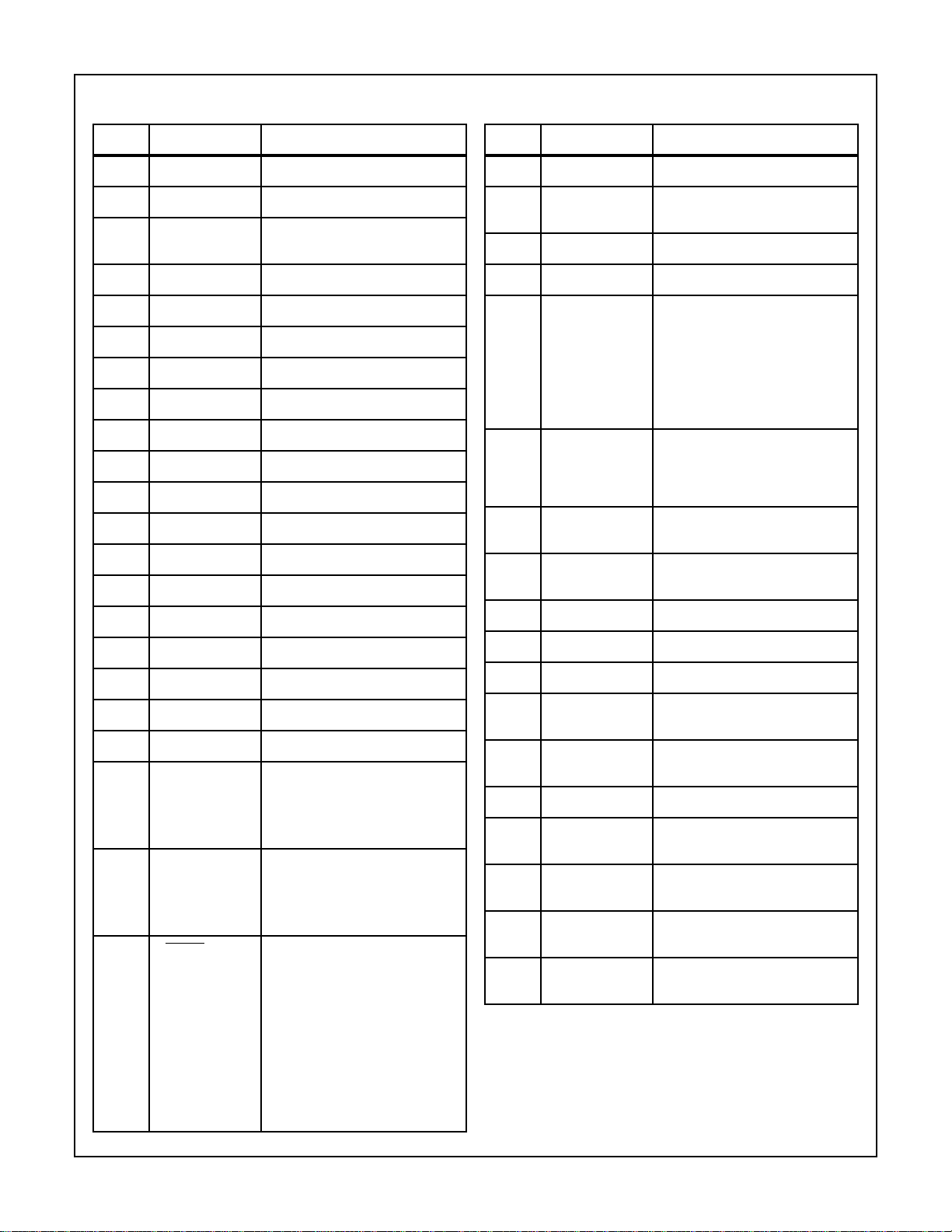
Pin Descriptions
ICL7129
PIN SYMBOL DESCRIPTION
1 OSC
2 OSC
1
3
3 ANNUNCIATOR
DRIVE
4B
5A
6F
, C1, CONT Output to display segments.
1
, G1, D
1
, E1, DP
1
Input to first clock inverter.
Output of second clock inverter.
Backplane squarewave output for
driving annunciators.
Output to display segments.
1
Output to display segments.
1
7B2, C2, LO BATT Output to display segments.
8A
9F
, G2, D
2
, E2, DP
2
Output to display segments.
2
Output to display segments.
2
10 B3, C3, MINUS Output to display segments.
11 A3, G3, D
12 F3, E3, DP
13 B4, C4, BC
14 A4, D4, G
15 F4, E4, DP
16 BP
17 BP
18 BP
19 V
3
2
1
DlSP
Output to display segments.
3
Output to display segments.
3
Output to display segments.
5
Output to display segments.
4
Output to display segments.
4
Backplane #3 output to display.
Backplane #2 output to display.
Backplane #1 output to display.
Negative rail for display drivers.
20 DP4/OR INPUT: When HI, turns on most
significant decimal point.
OUTPUT: Pulled HI when result
count exceeds ±19,999.
21 DP3/UR INPUT: Second most significant
decimal point on when HI.
OUTPUT: Pulled HI when result
count is less than ±1,000.
22 LATCH/HOLD INPUT: When floating, A/D converter
operates in the free-run mode. When
pulled HI, the last displayed reading is
held. When pulled LO, the result
counter contents are shown
incrementing during the de-integrate
phase of cycle.
OUTPUT: Negative going edge
occurs when the data latches are
updated. Can be used for converter
status signal.
PIN SYMBOL DESCRIPTION
23 V- Negative power supply terminal.
24 V+ Positive power supply terminal, and
positive rail for display drivers.
25 INT IN Input to integrator amplifier.
26 INT OUT Output of integrator amplifier.
27 CONTINUITY INPUT: When LO, continuity flag on
the display is off. When HI,
continuity flag is on.
OUTPUT: HI when voltage between
inputs is less than +200mV. LO
when voltage between inputs is
more than +200mV.
28 COMMON Sets common-mode voltage of 3.2V
below V+ for DE, 10X, etc., Can be
used as pre-regulator for external
reference.
29 C
+ Positive side of external reference
REF
capacitor.
30 C
- Negative side of external reference
REF
capacitor.
31 BUFFER Output of buffer amplifier.
32 IN LO Negative input voltage terminal.
33 IN HI Positive input voltage terminal.
34 REF HI Positive reference voltage input
terminal.
35 REF LO Negative reference voltage input
terminal.
36 DGND Ground reference for digital section.
37 RANGE 3µA pull-down for 200mV scale.
Pulled HIGH externally for 2V scale.
38 DP
2
Internal 3µA pull-down. When HI,
decimal point 2 will be on.
39 DP
1
Internal 3µA pull-down. When HI,
decimal point 1 will be on.
40 OSC2 Output of first clock inverter. Input of
second clock inverter.
3-34
 Loading...