

Intersil Corporation ICL7109CPL, ICL7109IDL, ICL7109IJL, ICL7109IPL, ICL7109MDL-883B Datasheet
1
®
November 2000
ICL7109
12-Bit, Microprocessor-
Compatible A/D Converter
Features
• 12-Bit Binary (Plus Polarity and Over-Range) Dual
Slope Integrating Analog-to-Digital Converter
• Byte-Organized, TTL Compatible Three-State Outputs
and UART Handshake Mode for Simple Parallel or
Serial Interfacing to Microprocessor Systems
• RUN/HOLD
Input and STATUS Output Can Be Used to
Monitor and Control Conversion Timing
• True Differential Input and Differential Reference
• Low Noise (Typ) . . . . . . . . . . . . . . . . . . . . . . . . 15µV
P-P
• Input Current (Typ) . . . . . . . . . . . . . . . . . . . . . . . . . .1pA
• Operates At Up to 30 Conversions/s
• On-Chip Oscillator Operates with Inexpensive 3.58MHz
TV Crystal Giving 7.5 Conversions/s for 60Hz Rejection. May Also Be Used with An RC Network Oscillator
for Other Clock Frequencies
Description
The ICL7109 is a high performance, CMOS, low power
integrating A/D converter designed to easily interface with
microprocessors.
The output data (12 bits, polarity and over-range) may be
directly accessed under control of two byte enable inputs and a
chip select input for a single parallel bus interface. A UART
handshake mode is provided to allow the ICL7109 to work with
industry-standard UARTs in providing serial data transmission.
The RUN/HOLD
input and STATUS output allow monitoring
and control of conversion timing.
The ICL7109 provides the user with the high accuracy, low
noise, low drift versatility and economy of the dual-slope
integrating A/D converter. Features like true differential input
and reference, drift of less than 1µV/
o
C, maximum input bias
current of 10pA, and typical power consumption of 20mW
make the ICL7109 an attractive per-channel alternative to
analog multiplexing for many data acquisition applications.
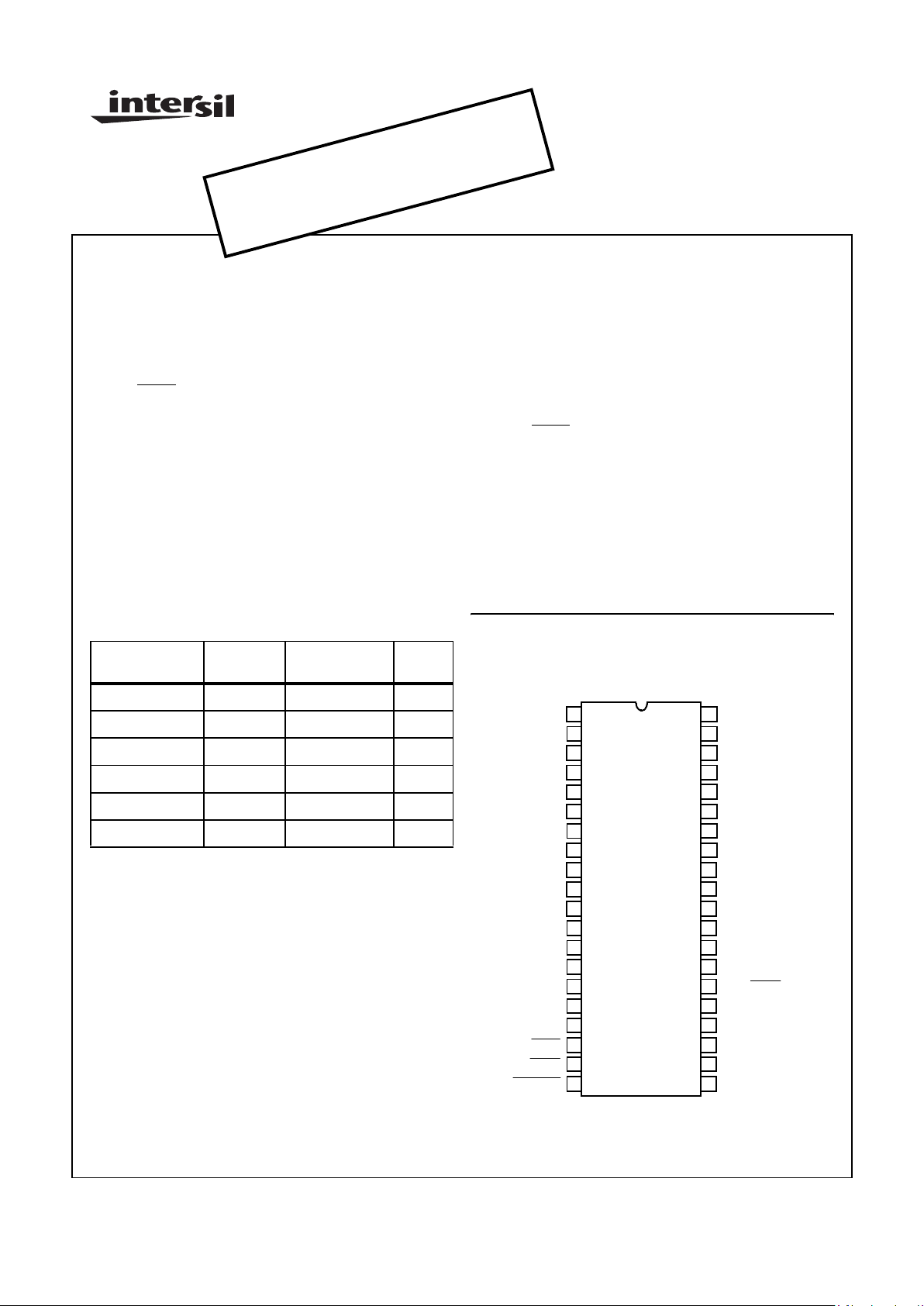
Pinout
ICL7109
(CERDIP, PDIP, SBDIP)
TOP VIEW
Part Number Information
PART NUMBER
TEMP.
RANGE (oC) PACKAGE
PKG.
NO.
ICL7109MDL -55 to 125 40 Ld SBDIP D40.6
ICL7109IDL -25 to 85 40 Ld SBDIP D40.6
ICL7109IJL -25 to 85 40 Ld CERDIP F40.6
ICL7109CPL 0 to 70 40 Ld PDIP E40.6
ICL7109MDL/883B -55 to 125 40 Ld SBDIP D40.6
ICL7109IPL -25 to 85 40 Ld PDIP E40.6
13
1
2
3
4
5
6
7
8
9
10
11
12
14
15
16
17
18
19
20
GND
STATUS
POL
OR
B12
B11
B10
B9
B8
B7
B6
B5
B4
B3
B2
B1
TEST
LBEN
HBEN
CE/LOAD
28
40
39
38
37
36
35
34
33
32
31
30
29
27
26
25
24
23
22
21
V+
REF IN -
REF CAP-
REF CAP+
REF IN+
IN HI
IN LO
COMMON
INT
AZ
BUF
REF OUT
V-
SEND
RUN/HOLD
BUF OSC OUT
OSC SEL
OSC OUT
OSC IN
MODE
File Number 3092.2
CAUTION: These devices are sensitive to electrostatic discharge; follow proper IC Handling Procedures.
1-888-INTERSIL or 321-724-7143
| Intersil (and design) is a registered trademark of Intersil Americas Inc.
Copyright © Intersil Americas Inc. 2002. All Rights Reserved
F
O
R
A
P
O
S
S
I
B
L
E
S
U
B
S
T
I
T
U
T
E
P
R
O
D
U
C
T
c
o
n
t
a
c
t
o
u
r
T
e
c
h
n
i
c
a
l
S
u
p
p
o
r
t
C
e
n
t
e
r
a
t
1
-
8
8
8
-
I
N
T
E
R
S
I
L
o
r
w
w
w
.
i
n
t
e
r
s
i
l
.
c
o
m
/
t
s
c
O
B
S
O
L
E
T
E
P
R
O
D
U
C
T
2
Absolute Maximum Ratings Thermal Information
Positive Supply Voltage (GND to V+). . . . . . . . . . . . . . . . . . . .+6.0V
Negative Supply Voltage (GND to V-) . . . . . . . . . . . . . . . . . . . . .-9V
Analog Input Voltage (Either Input) (Note 1) . . . . . . . . . . . . V+ to V-
Reference Input Voltage (Either Input) (Note 1) . . . . . . . . . . V+ to V-
Digital Input Voltage . . . . . . . . . . . . . . . . . . . . . . . . . . . . . (V+) +0.3V
Pins 2-27 (Note 2) . . . . . . . . . . . . . . . . . . . . . . . . . . . . . . GND -0.3V
Operating Conditions
Temperature Range
M Suffix . . . . . . . . . . . . . . . . . . . . . . . . . . . . . . . . . -55
o
C to 125oC
I Suffix . . . . . . . . . . . . . . . . . . . . . . . . . . . . . . . . . . . -25
o
C to 85oC
C Suffix . . . . . . . . . . . . . . . . . . . . . . . . . . . . . . . . . . . .0
o
C to 75oC
Thermal Resistance (Typical, Note 1) θ
JA
(oC/W) θJC (oC/W)
SBDIP Package. . . . . . . . . . . . . . . . . . . . 60 20
CERDIP Package . . . . . . . . . . . . . . . . . . 55 18
PDIP Package . . . . . . . . . . . . . . . . . . . . . 50 N/A
Maximum Junction Temperature (PDIP Package) . . . . . . . . . 150
o
C
Maximum Junction Temperature (CERDIP Package). . . . . . . 175
o
C
Maximum Storage Temperature Range . . . . . . . . . . -65
o
C to 150oC
Maximum Lead Temperature (Soldering 10s Max). . . . . . . . . 300
o
C
CAUTION: Stresses above those listed in “Absolute Maximum Ratings” may cause permanent damage to the device. This is a stress only rating and operation
of the device at these or any other condition s above those indicated in the operational sections of this specification is not implied.
NOTE:
1. θ
JA
is measured with the component mounted on an evaluation PC board in free air.
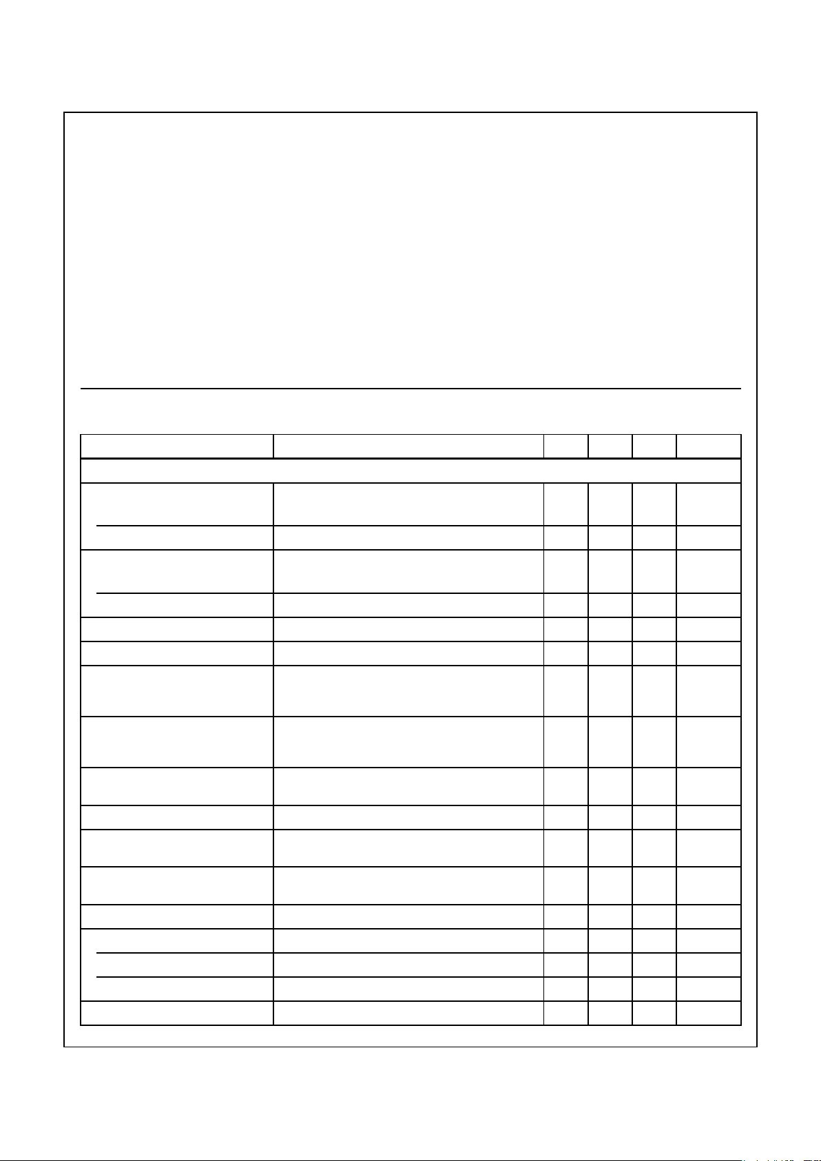
Analog Electrical Specifications V+ = +5V, V- = -5V, GND = 0V, T
A
= 25oC, f
CLK
= 3.58MHz,
Unless Otherwise Specified
PARAMETER TEST CONDITIONS MIN TYP MAX UNIT
SYSTEM PERFORMANCE
Oscillator Output Current
High, O
OH
V
OUT
= 2.5V - 1 - mA
Low, O
OL
V
OUT
= 2.5V - 1.5 - mA
Buffered Oscillator Output Current
High, BO
OH
V
OUT
= 2.5V - 2 - mA
Low, BO
OL
V
OUT
= 2.5V - 5 - mA
Zero Input Reading V
IN
= 0.0000V, V
REF
= 204.8mV -0000 ±0000 +0000 Counts
Ratiometric Error V
lN
= V
REF
, V
REF
= 204.8mV (Note 7) -3 - 0 Counts
Non-Linearity Full Scale = 409.6mV to 2.048mV
Maximum Deviation from Best Straight Line Fit, Over
Full Operating Temperature Range (Notes 4 and 6)
-1 ±0.2 +1 Counts
Rollover Error Full Scale = 409.6mV to 2.048V
Difference in Reading for Equal Positive and Negative
Inputs Near Full Scale (Notes 5 and 6), R
1
= 0Ω
-1 ±0.2 +1 Counts
Linearity Full-Scale = 200mV or Full Scale = 2V Maximum
Deviation from Best Straight Line Fit (Note 4)
- ±0.2 ±1 Counts
Common Mode Rejection Ratio, CMRR V
CM
= ±1V, VIN = 0V, Full Scale = 409.6mV - 50 - µV/V
Input Common Mode Range, VCMR Input HI, Input LO, Common (Note 4) (V-)
+2.0
-(V+)
-2.0
V
Noise, eN V
IN
= 0V, Full-Scale = 409.6mV
(Peak-to-Peak Value Not Exceeded 95% of Time)
-15- µV
Leakage Current Input, I
ILK
VlN = 0V, All Devices at 25oC (Note 4) - 1 10 pA
ICL7109CPL 0
o
C to 70oC (Note 4) - 20 100 pA
ICL7109IDL -25
o
C to 85oC (Note 4) - 100 250 pA
ICL7109MDL -55
o
C to 125oC-2100nA
Zero Reading Drift V
lN
= 0V, R1 - 0Ω (Note 4) - 0.2 1 µV/oC
ICL7109
3
Scale Factor Temperature Coefficient VIN = 408.9mV = > 77708 Reading Ext. Ref. 0ppm/oC
(Note 4)
- 1 5 ppm/oC
REFERENCE VOLTAGE
Ref Out Voltage, V
REF
Referred to V+, 25kΩ Between V+ and REF OUT -2.4 -2.8 -3.2 V
Ref Out Temperature Coefficient 25kΩ Between V+ and REF OUT (Note 4) - 80 - ppm/
o
C
POWER SUPPLY CHARACTERISTICS
Supply Current V+ to GND, I+ V
IN
= 0V, Crystal Osc 3.58MHz Test Circuit - 700 1500 µA
Supply Current V+ to V-, I
SUPP
Pins 2 - 21, 25, 26, 27, 29; Open - 700 1500 µA
Digital Electrical Specifications V+ = +5V, V- = -5V, GND = 0V, T
A
= 25oC, Unless Otherwise Specified
PARAMETER TEST CONDITIONS MIN TYP MAX UNIT
DIGITAL OUTPUTS
Output High Voltage, V
OH
I
OUT
= 100µA Pins 2 - 16, 18, 19, 20 3.5 4.3 - V
Output Low Voltage, V
OL
I
OUT
= 1.6mA Pins 2 - 16, 18, 19, 20 - ±0.20 ±0.40 V
Output Leakage Current Pins 3 - 16 High Impedance - ±0.01 ±1 µA
Control I/O Pullup Current Pins 18, 19, 20 V
OUT
= V+ -3V MODE Input at GND
(Note 4)
-5- µA
Control I/O Loading HBEN
Pin 19 LBEN Pin 18 (Note 4) - − 50 pF
DIGITAL INPUTS
Input High Voltage, V
IH
Pins 18 - 21, 26, 27 Referred to GND 3.0 - - V
Input Low Voltage, V
IL
Pins 18 - 21, 26, 27 Referred to GND - - 1 V
Input Pull-Up Current Pins 26, 27 V
OUT
= (V+) -3V - 5 - µA
Input Pull-Up Current Pins 17, 24 V
OUT
= (V+) -3V - 25 - µA
Input Pull-Down Current Pin 21 V
OUT
= GND +3V - 5 - µA
TIMING CHARACTERISTICS
MODE Input Pulse Width, t
W
(Note 4) 50 - - ns
NOTES:
1. Input voltages may exceed the supply voltages provided the input current is limited to ±100µA.
2. Due to the SCR structure inherent in the process used to fabricate these devices, connecting any digital inputs or outputs to voltages
greater than V+ or less than GND may cause destructive device latchup. For this reason it is recommended that no inputs from sources
other than the same power supply be applied to the ICL7109 before its power supply is established, and that in multiple supply systems
the supply to the ICL7109 be activated first.
3. This limit refers to that of the package and will not be obtained during normal operation.
4. This parameter is not production tested, but is guaranteed by design.
5. Roll-over error for T
A
= -55oC to 125oC is ±10 counts (Max).
6. A full scale voltage of 2.048V is used because a full scale voltage of 4.096V exceeds the devices Common Mode Voltage Range.
7. For CERDIP package the Ratiometric error can be -4 (Min).
Analog Electrical Specifications V+ = +5V, V- = -5V, GND = 0V, T
A
= 25oC, f
CLK
= 3.58MHz,
Unless Otherwise Specified (Continued)
PARAMETER TEST CONDITIONS MIN TYP MAX UNIT
ICL7109
4
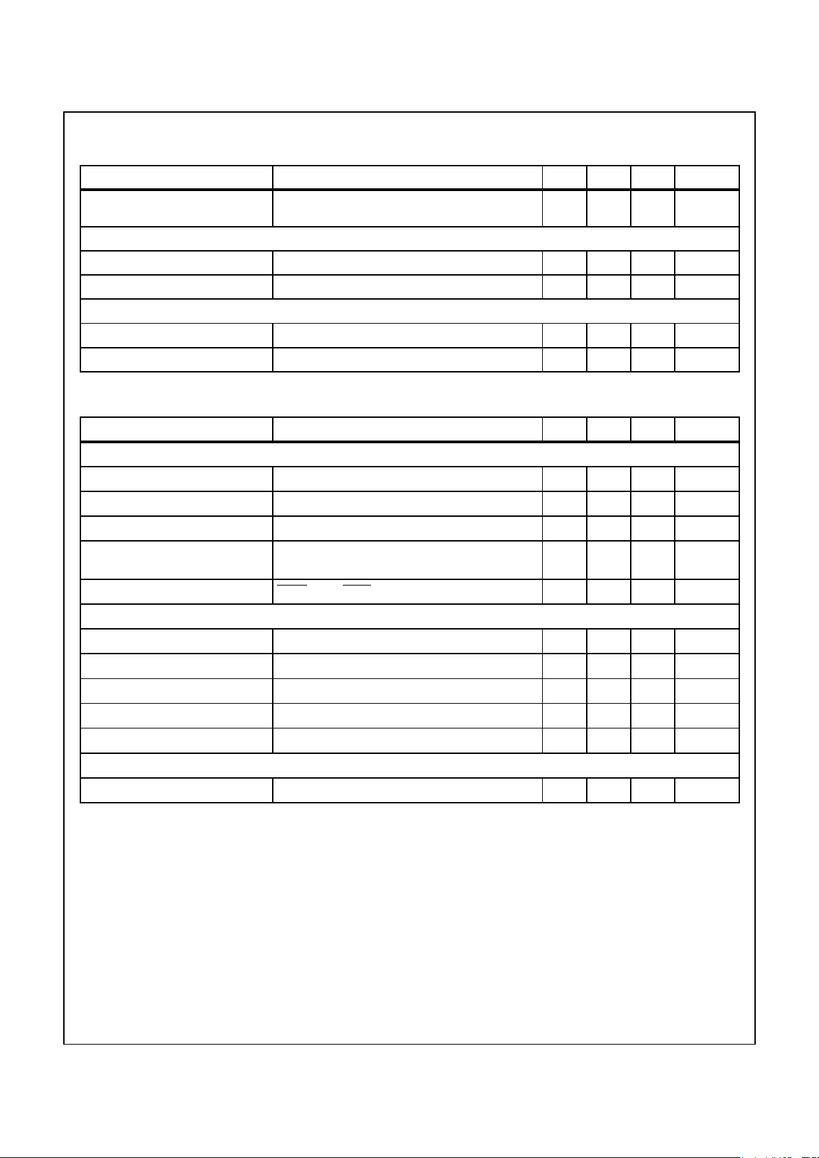
Pin Descriptions
PIN SYMBOL DESCRIPTION
1 GND Digital Ground, 0V. Ground return for all digital logic.
2 STATUS Output High during integrate and deintegrate until data is latched. Output Low when analog section
is in Auto-Zero configuration.
3 POL Polarity - HI for positive input. Three-State Output Data Bits
4 OR Overrange - HI if overranged. Three-State Output Data Bits
5 B12 Bit 12 (Most Significant Bit) Three-State Output Data Bits
6 B11 Bit 11 High = True Three-State Output Data Bits
7 B10 Bit 10 High = True Three-State Output Data Bits
8 B9 Bit 9 High = True Three-State Output Data Bits
9 B8 Bit 8 High = True Three-State Output Data Bits
10 B7 Bit 7 High = True Three-State Output Data Bits
11 B6 Bit 6 High = True Three-State Output Data Bits
12 B5 Bit 5 High = True Three-State Output Data Bits
13 B4 Bit 4 High = True Three-State Output Data Bits
14 B3 Bit 3 High = True Three-State Output Data Bits
15 B2 Bit 2 High = True Three-State Output Data Bits
16 B1 Bit 1 (Least Significant Bit) Three-State Output Data Bits
17 TEST Input High - Normal Operation. Input Low - Forces all bit outputs high. Note: This input is used for
test purposes only. Tie high if not used.
18 LBEN
Low Byte Enable - With Mode (Pin 21) low, and CE/LOAD (Pin 20) low, taking this pin low activates
low order byte outputs B1 through B8.
With Mode (Pin 21) high, this pin serves as a low byte flag output used in handshake mode.
See Figures 7, 8, 9.
19 HBEN
High Byte Enable - With Mode (Pin 21) low, and CE/LOAD (Pin 20) low, taking this pin low activates
high order byte outputs B9 through B12, POL, OR.
With Mode (Pin 21) high, this pin serves as a high byte flag output used in handshake mode.
See Figures 7, 8, 9.
20 CE/LOAD
Chip Enable Load - With Mode (Pin 21) low. CE/LOAD serves as a master output enable. When
high, B1 through B12, POL, OR outputs are disabled.
With Mode (Pin 21) high, this pin serves as a load strobe used in handshake mode.
See Figures 7, 8, 9.
21 MODE Input Low - Direct output mode where CE/LOAD
(Pin 20), HBEN (Pin 19) and LBEN (Pin 18) act as
inputs directly controlling byte outputs.
Input Pulsed High - Causes immediate entry into handshake mode and output of data as in Figure 9.
Input High - Enables CE/LOAD
(Pin 20), HBEN (Pin 19), and LBEN (Pin 18) as outputs, handshake
mode will be entered and data output as in Figures 7 and 8 at conversion completion.
22 OSC IN Oscillator Input
23 OSC OUT Oscillator Output
ICL7109
5
24 OSC SEL Oscillator Select - Input high configures OSC IN, OSC OUT, BUF OSC OUT as RC oscillator - clock
will be same phase and duty cycle as BUF OSC OUT.
Input low configures OSC IN, OSC OUT for crystal oscillator - clock frequency will be 1/58 of
frequency at BUF OSC OUT.
25 BUF OSC OUT Buffered Oscillator Output
26 RUN/HOLD
Input High - Conversions continuously performed every 8192 clock pulses.
Input Low - Conversion in progress completed, converter will stop in Auto-Zero 7 counts before
integrate.
27 SEND Input - Used in handshake mode to indicate ability of an external device to accept data. Connect to
+5V if not used.
28 V- Analog Negative Supply - Nominally -5V with respect to GND (Pin 1).
29 REF OUT Reference Voltage Output - Nominally 2.8V down from V+ (Pin 40).
30 BUFFER Buffer Amplifier Output.
31 AUTO-ZERO Auto-Zero Node - Inside foil of C
AZ
.
32 INTEGRATOR Integrator Output - Outside foil of C
INT
.
33 COMMON Analog Common - System is Auto-Zeroed to COMMON.
34 INPUT LO Differential Input Low Side.
35 INPUT HI Differential Input High Side.
36 REF IN + Differential Reference Input Positive.
37 REF CAP + Reference Capacitor Positive.
38 REF CAP- Reference Capacitor Negative.
39 REF IN- Differential Reference Input Negative.
40 V+ Positive Supply Voltage - Nominally +5V with respect to GND (Pin 1).
NOTE: All digital levels are positive true.
Pin Descriptions (Continued)
PIN SYMBOL DESCRIPTION
ICL7109

6
Design Information Summary Sheet
• OSCILLATOR FREQUENCY
f
OSC
= 0.45/RC
C
OSC
> 50pF; R
OSC
> 50kΩ
f
OSC
(Typ) = 60kHz
or
f
OSC
(Typ) = 3.58MHz Crystal
• OSCILLATOR PERIOD
t
OSC
= RC/0.45
t
OSC
= 1/3.58MHz (Crystal)
• INTEGRATION CLOCK FREQUENCY
f
CLOCK
= f
OSC
(RC Mode)
f
CLOCK
= f
OSC
/58 (Crystal)
t
CLOCK
= 1/f
CLOCK
• INTEGRATION PERIOD
t
INT
= 2048 x t
CLOCK
• 60/50Hz REJECTION CRITERION
t
INT/t60Hz
or t
lNT/t50Hz
= Integer
• OPTIMUM INTEGRATION CURRENT
I
INT
= 20µA
• FULL-SCALE ANALOG INPUT VOLTAGE
V
lNFS
Typically = 200mV or 2V
• INTEGRATE RESISTOR
• INTEGRATE CAPACITOR
• INTEGRATOR OUTPUT VOLTAGE SWING
•V
INT
MAXIMUM SWING
(V- + 0.5V) < V
INT
< (V+ - 0.5V)
V
INT
(Typ) = 2V
• DISPLAY COUNT
• CONVERSION CYCLE
t
CYC
= t
CL0CK
x 8192
(In Free Run Mode, Run/HOLD
= 1)
when f
CLOCK
= 60kHz, t
CYC
= 133ms
• COMMON MODE INPUT VOLTAGE
(V- + 2.0V) < V
lN
< (V+ - 2V)
• AUTO-ZERO CAPACITOR
0.01µF < C
AZ
< 1µF
• REFERENCE CAPACITOR
0.1µF < C
REF
< 1µF
•V
REF
Biased between V+ and VV
REF
≅ V+ - 2.8V
Regulation lost when V+ to V- ≤ 6.4V.
If V
REF
is not used, float output pin.
• POWER SUPPLY: DUAL ±5.0V
V+ = +5V to GND
V- = -5V to GND
• OUTPUT TYPE
Binary Amplitude with Polarity and Overrange Bits
Tips: Always tie TEST pin HIGH.
Don’t leave any inputs floating.
R
INT
V
INFS
I
INT
------ ----- ---- --=
C
INT
t
INT
()I
INT
()
V
INT
--------------------------------=
V
INT
t
INT
()I
INT
()
C
INT
--------------------------------=
COUNT 2048
V
IN
V
REF
-----------------×=
ICL7109
7
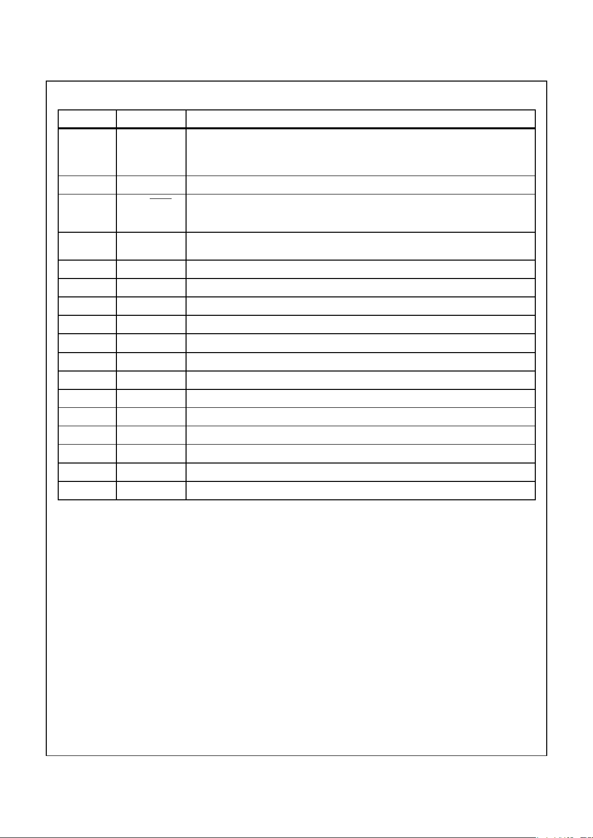
Typical Integrator Amplifier Output Waveform (INT Pin)
AUTO ZERO PHASE
(COUNTS)
6143 - 2048
INTEGRATE
PHASE FIXED
2048 COUNTS
DE-INTEGRATE PHASE
0 - 4095 COUNTS
TOTAL CONVERSION TIME = 8192 x t
CLOCK
(IN FREE-RUN MODE)
FIGURE 1A. TYPICAL CONNECTION DIAGRAM UART INTERFACE-TO TRANSMIT LATEST RESULT, SEND ANY WORD TO UART
18
1
25
2
19
17
21
20
27
GND
BUF OSC
STATUS
HBEN
3 - 8
B9 - B12, POL,OR
9 - 16
TEST
LBEN
MODE
CE/LOAD
SEND
28
40
39
38
37
36
35
34
33
32
31
30
29
26
24
23
22
V+
REF IN -
REF CAP-
REF CAP+
REF IN+
IN HI
IN LO
COMMON
INT
AZ
BUF
REF OUT
V-
RUN/HOLD
OSC SEL
OSC OUT
OSC IN
GND
GND
+5V
1µF
0.01µF
0.33µF
0.15µF
C
AZ
C
INT
R
INT
1MΩ
3.58MHz
CRYSTAL
-
+
+
INPUT
GND
EXTERNAL
REFERENCE
-5V
GND
-
20kΩ 0.2V REF
200kΩ 2V REF
+5V OR OPEN
OUT
/
/
6
8
B1 - B8
1
2
3
4
13
14
15
16
20
25
V+
OSC CONTROL
GND
RRD
5 - 12
PE
FE
OE
SFD
RRI
TRO
18
40
17
39
38
37
36
35
34
31
24
19
23
22
21
XTAL
XTAL
EPE
CLS1
CLS2
SBS
PI
CLR
26 - 33
TRE
DRR
DR
TBRL
TBRE
MR
GND
GND
TBR 1 - 8
+5V
+5V
8
/
GND
1000pF
RBR 1 - 8
SERIAL
OUTPUT
SERIAL
INPUT
+5V
+5V
+5V
IM6403
CMOS UART
ICL7109
CMOS A/D CONVERTER
FOR LOWEST POWER CONSUMPTION
TBR1 - TBR8 INPUTS SHOULD HAVE 100kΩ
PULLUP RESISTORS TO +5V
+5V
ICL7109
8
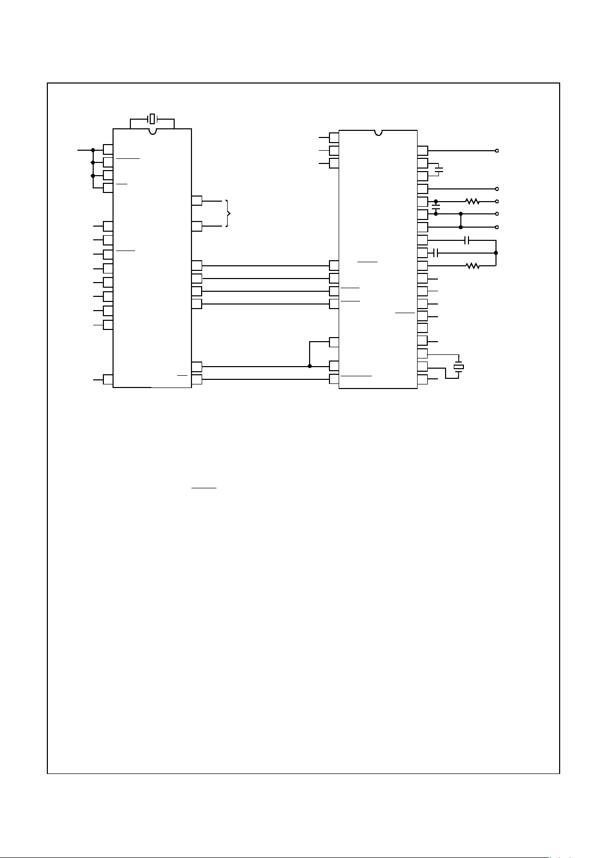
Detailed Description
Analog Section
Figure 2 shows the equivalent circuit of the Analog Section
for the ICL7109. When the RUN/HOLD
input is left open or
connected to V+, the circuit will perform conversions at a
rate determined by the clock frequency (8192 clock periods
per cycle). Each measurement cycle is divided into three
phases as shown in Figure 3. They are (1) auto-zero (A-Z),
(2) signal integrate (INT) and (3) de-integrate (DE).
Auto-Zero Phase
During auto-zero three things happen. First, input high and
low are disconnected from the pins and internally shorted to
analog COMMON. Second, the reference capacitor is
charged to the reference voltage. Third, a feedback loop is
closed around the system to charge the auto-zero capacitor
C
AZ
to compensate for offset voltages in the buffer amplifier,
integrator, and comparator. Since the comparator is included
in the loop, the A-Z accuracy is limited only by the noise of
the system. In any case, the offset referred to the input is
less than 10µV.
Signal Integrate Phase
During signal integrate, the auto-zero loop is opened, the
internal short is removed, and the internal input high and low
are connected to the external pins. The converter then
integrates the differential voltage between IN HI and IN LO
for a fixed time. This differential voltage can be within a wide
common mode range of the inputs. At the end of this phase,
the polarity of the integrated signal is determined.
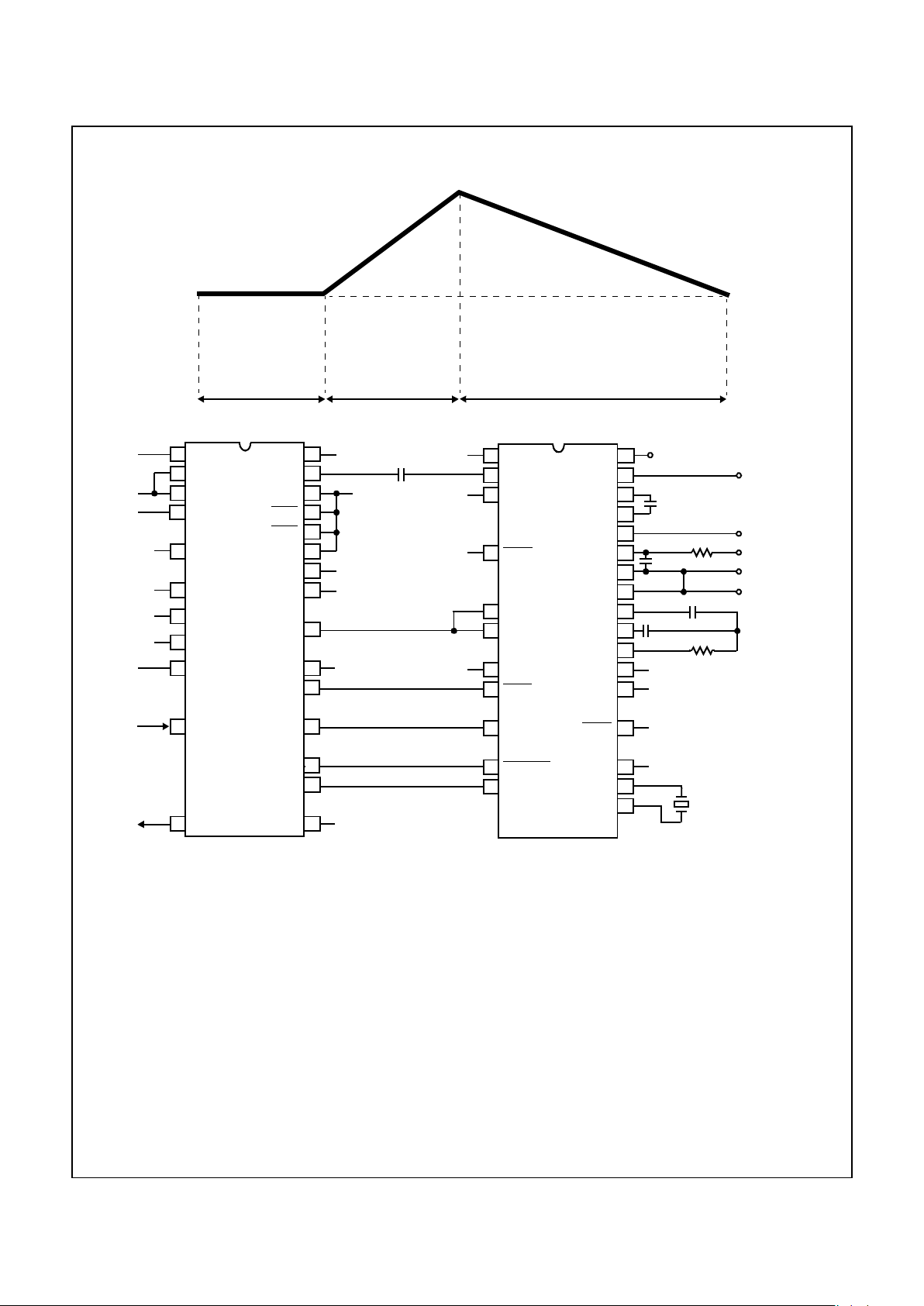
FIGURE 1B. TYPICAL CONNECTION DIAGRAM PARALLEL INTERFACE WITH 8048 MICROCOMPUTER
FIGURE 1.
9
25
26
40
39
/
5
20
5
6
17
26
19
18
40
1
2
V+
TEST
3 - 8
B9 - B12,
9 - 16
STATUS
HBEN
CE/LOAD
28
39
38
37
36
35
34
33
32
31
30
29
26
24
23
21
REF IN -
REF CAP-
REF CAP+
REF IN+
IN HI
IN LO
COMMON
INT
AZ
BUF
REF OUT
V-
RUN/HOLD
OSC SEL
OSC OUT
OSC IN
GND
GND
1µF
0.01µF
0.33µF
0.15µF
C
AZ
C
INT
R
INT
1MΩ
3.58MHz
CRYSTAL
-
+
+
INPUT
GND
EXTERNAL
REFERENCE
-5V
GND
-
20kΩ 0.2V REF
200kΩ 2V REF
+5V OR OPEN
GND
/
/
6
8
B1 - B8
1
4
7
8
11
20
XTAL1
TO
RESET
EA
WR
ALE
GND
28
30
29
27
10
XTAL2
P12
P11
P10
RD
P13
+5V
8
/
27
25
22
MODE
SEND
BUFF OSC OUT
+5V
+5V
SS
INT
2
RUN/HOLD
LBEN
POL,OR
12 - 19
DB0 - DB7
31 - 34
P14 - P17
35 - 38
P20 - P27
/
8
21 - 24
OTHER
I/O
GND
PSEN
GND
PROG
V
DD
V
CC
+5V
TL
+5V
+5V
+5V
ICL7109
8748/9048
3
+5V
ICL7109

9
De-Integrate Phase
The final phase is de-integrate, or reference integrate. Input
low is internally connected to analog COMMON and input
high is connected across the previously charged (during
auto-zero) reference capacitor. Circuitry within the chip
ensures that the capacitor will be connected with the correct
polarity to cause the integrator output to return to zero crossing (established in Auto-Zero) with a fixed slope. The time
required for the output to return to zero is proportional to the
input signal.
Differential Input
The input can accept differential voltages anywhere within the
common mode range of the input amplifier, or specifically from
1V below the positive supply to 1.5V above the negative supply. In this range, the system has a CMRR of 86dB typical.
However, care must be exercised to assure the integrator output does not saturate. A worst case condition would be a large
positive common mode voltage with a near full-scale negative
differential input voltage. The negative input signal drives the
integrator positive when most of its swing has been used up
by the positive common mode voltage. For these critical applications the integrator output swing can be reduced to less
than the recommended 4V full scale swing with little loss of
accuracy. The integrator output can swing to within 0.3V of
either supply without loss of linearity.
The ICL7109 has, however, been optimized for operation
with analog common near digital ground. With power supplies of +5V and -5V, this allows a 4V full scale integrator
swing positive or negative thus maximizing the performance
of the analog section.
Differential Reference
The reference voltage can be generated anywhere within the
power supply voltage of the converter. The main source of
common mode error is a roll-over voltage caused by the
reference capacitor losing or gaining charge to stray capacity
on its nodes. If there is a large common mode voltage, the reference capacitor can gain charge (increase voltage) when
called up to deintegrate a positive signal but lose charge
(decrease voltage) when called up to deintegrate a negative
input signal. This difference in reference for positive or
negative input voltage will give a roll-over error. However, by
selecting the reference capacitor large enough in comparison
to the stray capacitance, this error can be held to less than 0.5
count worst case. (See Component Value Selection.)
The roll-over error from these sources is minimized by having
the reference common mode voltage near or at analog
COMMON.
Component Value Selection
For optimum performance of the analog section, care must
be taken in the selection of values for the integrator capacitor and resistor, auto-zero capacitor, reference voltage, and
conversion rate. These values must be chosen to suit the
particular application.
The most important consideration is that the integrator output swing (for full-scale input) be as large as possible. For
example, with ±5V supplies and COMMON connected to
+
-
+
DE-DE+
C
INT
C
AZ
R
INT
BUFFER
A-Z INT
-
+
A-Z
IN HI
COMMON
IN LO
35
33
34
DE- DE+
INT
A-Z
37
C
REF
+
36
REF IN+
C
REF
REF IN-
39
A-Z A-Z
38
C
REF
-
30 31 32
TO ZERO CROSS
DETECTOR
DIGITAL SECTION
A-Z
INTEGRATOR
INT
DE(±)
BUFFER
COMPARATOR
REF OUT
6.2V
29 28 40
10µA
V- V+
AZ
INT
DE+
DE-
FROM CONTROL
LOGIC
DIGITAL SECTION
-
+
FIGURE 2. ANALOG SECTION OF ICL7109
ICL7109
Teflon™ is a trademark of DuPont Corporation

10
GND, the normal integrator output swing at full scale is ±4V.
Since the integrator output can go to 0.3V from either supply
without significantly affecting linearity, a 4V integrator output
swing allows 0.7V for variations in output swing due to component value and oscillator tolerances. With ±5V supplies
and a common mode range of ±1V required, the component
values should be selected to provide ±3V integrator output
swing. Noise and roll-over will be slightly worse than in the
±4V case. For larger common mode voltage ranges, the integrator output swing must be reduced further. This will
increase both noise and roll-over errors. To improve the performance, supplies of ±6V may be used.
Integrating Resistor
Both the buffer amplifier and the integrator have a class A output
stage with 100µA of quiescent current. They supply 20µA of drive
current with negligible nonlinearity. The integrating resistor
should be large enough to remain in this very linear region over
the input voltage range, but small enough that undue leakage
requirements are not placed on the PC board. For 409.6mV fullscale, 200kΩ is near optimum and similarly a 20kΩ for a
409.6mV scale. For other values of full scale voltage, R
INT
should be chosen by the relation :
Integrating Capacitor
The integrating capacitor C
INT
should be selected to give the
maximum voltage swing that ensures tolerance build-up will
not saturate the integrator swing (approximately. 0.3V from
either supply). For the ICL7109 with ±5V supplies and analog
common connected to GND, a ±3.5V to ±4V integrator output
swing is nominal. For 7
1
/2 conversions per second (61.72kHz
clock frequency) as provided by the crystal oscillator, nominal
values for C
INT
and CAZ are 0.15µF and 0.33µF, respectively. If different clock frequencies are used, these values
should be changed to maintain the integrator output swing. In
general, the value C
INT
is given by:
.
An additional requirement of the integrating capacitor is that
it have low dielectric absorption to prevent roll-over errors.
While other types of capacitors are adequate for this application, polypropylene capacitors give undetectable errors at
The integrating capacitor should have a low dielectric
absorption to prevent roll-over errors. While other types may
be adequate for this application, polypropylene capacitors
give undetectable errors at reasonable cost up to 85
o
C.
Teflon™ capacitors are recommended for the military temperature range. While their dielectric absorption characteristics vary somewhat from unit to unit, selected devices should
give less than 0.5 count of error due to dielectric absorption.
Auto-Zero Capacitor
The size of the auto-zero capacitor has some influence on
the noise of the system: a smaller physical size and a larger
capacitance value lower the overall system noise. However,
C
AZ
cannot be increased without limits since it, in parallel
with the integrating capacitor forms an R-C time constant
that determines the speed of recovery from overloads and
the error that exists at the end of an auto-zero cycle. For
409.6mV full scale where noise is very important and the
integrating resistor small, a value of C
AZ
twice C
INT
is optimum. Similarly for 4.096V full scale where recovery is more
important than noise, a value of C
AZ
equal to half of C
INT
is
recommended.
For optimal rejection of stray pickup, the outer foil of C
AZ
should be connected to the R-C summing junction and the
inner foil to pin 31. Similarly the outer foil of C
INT
should be
connected to pin 32 and the inner foil to the R-C summing
junction. Teflon, or equivalent, capacitors are recommended
above 85
o
C for their low leakage characteristics.
Reference Capacitor
A 1µF capacitor gives good results in most applications.
However, where a large reference common mode voltage
exists (i.e., the reference low is not at analog common) and
a 409.6mV scale is used, a large value is required to prevent
roll-over error. Generally 10µF will hold the roll-over error to
0.5 count in this instance. Again, Teflon, or equivalent
capacitors should be used for temperatures above 85
o
C for
their low leakage characteristics.
R
INT
full scale voltage
20µA
--------------------------------------------·.=
C
INT
2048 clock period×()20µA()
integrator output voltage swing
---------------------------------------------------------------------------------=
ICL7109

11
Reference Voltage
The analog input required to generate a full scale output of
4096 counts is V
IN
= 2V
REF
. For normalized scale, a refer-
ence of 2.048V should be used for a 4.096V full scale, and
204.8mV should be used for a 0.4096V full scale. However,
in many applications where the A/D is sensing the output of
a transducer, there will exist a scale factor other than unity
between the absolute output voltage to be measured and a
desired digital output. For instance, in a weighing system,
the designer might like to have a full scale reading when the
voltage from the transducer is 0.682V. Instead of driving the
input down to 409.6mV, the input voltage should be measured directly and a reference voltage of 0.341V should be
used. Suitable values for integrating resistor and capacitor
are 33kΩ and 0.15µF. This avoids a divider on the input.
Another advantage of this system occurs when a zero reading is desired for non-zero input. Temperature and weight
measurements with an offset or tare are examples. The offset may be introduced by connecting the voltage output of
the transducer between common and analog high, and the
offset voltage between common and analog low, observing
polarities carefully. However, in processor-based systems
using the ICL7109, it may be more efficient to perform this
type of scaling or tare subtraction digitally using software.
Reference Sources
The stability of the reference voltage is a major factor in the
overall absolute accuracy of the converter. The resolution of
the ICL7109 at 12 bits is one part in 4096, or 244ppm. Thus
if the reference has a temperature coefficient of 80ppm/
o
C
(onboard reference) a temperature difference of 3
o
C will
introduce a one-bit absolute error.
For this reason, it is recommended that an external highquality reference be used where the ambient temperature is
not controlled or where high-accuracy absolute measure-
ments are being made.
The ICL7109 provides a REFerence OUTput (Pin 29) which
may be used with a resistive divider to generate a suitable
reference voltage. This output will sink up to about 20mA
without significant variation in output voltage, and is provided
with a pullup bias device which sources about 10µA. The
output voltage is nominally 2.8V below V+, and has a temperature coefficient of ±80ppm/
o
C (Typ). When using the
onboard reference, REF OUT (Pin 29) should be connected
to REF- (Pin 39), and REF+ should be connected to the
wiper of a precision potentiometer between REF OUT and
V+. The circuit for a 204.8mV reference is shown in the test
circuit. For a 2.048mV reference, the fixed resistor should be
removed, and a 25kΩ precision potentiometer between REF
OUT and V+ should be used.
Note that if Pins 29 and 39 are tied together and Pins 39 and
40 accidentally shorted (e.g., during testing), the reference
supply will sink enough current to destroy the device. This can
be avoided by placing a 1kΩ resistor in series with Pin 39.
Detailed Description
Digital Section
The digital section includes the clock oscillator and scaling
circuit, a 12-bit binary counter with output latches and TTLcompatible three-state output drivers, polarity, over-range
and control logic, and UART handshake logic, as shown in
Figure 4.
Throughout this description, logic levels will be referred to as
“low” or “high”. The actual logic levels are defined in the Electrical Specifications Table. For minimum power consumption,
all inputs should swing from GND (low) to V+ (high). Inputs
driven from TTL gates should have 3-5kΩ pullup resistors
MODE Input The MODE input is used to control the output mode of the
AZ PHASE I INT PHASE II DEINT PHASE III AZ
INTERNAL CLOCK
INTERNAL LATCH
STATUS OUTPUT
INTEGRATOR
OUTPUT
POLARITY
DETECTED
ZERO CROSSING
OCCURS
ZERO CROSSING
DETECTED
4096 COUNTS
MAX
FIXED 2048
COUNTS
2048 COUNTS
MINIMUM
NUMBER OF COUNTS TO ZERO CROSSING
PROPORTIONAL TO V
IN
AFTER ZERO CROSSING
ANALOG SECTION WILL
BE IN AUTOZERO
CONFIGURATION
FIGURE 3. CONVERSION TIMING (RUN/HOLD PIN HIGH)
ICL7109

12
converter. When the MODE pin is low or left open (this input
is provided with a pulldown resistor to ensure a low level
when the pin is left open), the converter is in its “Direct” output mode, where the output data is directly accessible under
the control of the chip and byte enable inputs. When the
MODE input is pulsed high, the converter enters the UART
handshake mode and outputs the data in two bytes, then
returns to “direct” mode. When the MODE input is left high,
the converter will output data in the handshake mode at the
end of every conversion cycle. (See section entitled “Handshake Mode” for further details).
STATUS Output
During a conversion cycle, the STATUS output goes high at
the beginning of Signal Integrate (Phase II), and goes low
one-half clock period after new data from the conversion has
been stored in the output latches. See Figure 3 for of this timing. This signal may be used as a “data valid” flag (data never
changes while STATUS is low) to drive interrupts, or for
monitoring the status of the converter.
RUN/HOLD
Input
When the RUN/HOLD
input is high, or left open, the circuit will
continuously perform conversion cycles, updating the output
latches after zero crossing during the Deintegrate (Phase III)
portion of the conversion cycle (See Figure 3). In this mode of
operation, the conversion cycle will be performed in 8192
clock periods, regardless of the resulting value.
FIGURE 4. DIGITAL SECTION
TEST
LATCH
CLOCK
POLOR 12111098 7 65432 1
17 3 4 5 6 7 8 9 10 11 12 13 14 15 16
226222324252127
STATUS RUN/ OSC OSC OSC BUF MODE SEND
HOLD
IN OUT SEL OSC
OUT
LOW ORDER
BYTE OUTPUTS
BB BBB B BBBBB B
GND
1
18
19
20
LBEN
HBEN
CE/LOAD
TO
ANALOG
SECTION
COMP OUT
AZ
INT
DEINT (+)
DEINT (-)
CONVERSION
CONTROL LOGIC
OSCILLATOR
AND CLOCK
CIRCUITRY
HIGH ORDER
BYTE OUTPUTS
12-BIT COUNTER
14 LATCHES
14 THREE-STATE OUTPUTS
HANDSHAKE
LOGIC
ICL7109

13
If RUN/HOLD
goes low at any time during Deintegrate (Phase
III) after the zero crossing has occurred, the circuit will immediately terminate Deintegrate and jump to Auto-Zero. This feature can be used to eliminate the time spent in Deintegrate
after the zero-crossing. If RUN/HOLD
stays or goes low, the
converter will ensure minimum Auto-Zero time, and then wait
in Auto-Zero until the RUN/HOLD
input goes high. The converter will begin the Integrate (Phase II) portion of the next
conversion (and the STATUS output will go high) seven clock
periods after the high level is detected at RUN/HOLD
. See
Figure 5 for details.
Using the RUN/HOLD
input in this manner allows an easy
“convert on demand” interface to be used. The converter may
be held at idle in auto-zero with RUN/HOLD
low. When
RUN/HOLD
goes high the conversion is started, and when
the STATUS output goes low the new data is valid (or transferred to the UART; see Handshake Mode). RUN/HOLD
may
now be taken low which terminates deintegrate and ensures a
minimum Auto-Zero time before the next conversion.
Alternately, RUN/HOLD
can be used to minimize conversion
time by ensuring that it goes low during Deintegrate, after zero
crossing, and goes high after the hold point is reached. The
required activity on the RUN/HOLD
input can be provided by
connecting it to the Buffered Oscillator Output. In this mode
the conversion time is dependent on the input value
measured. Also refer to Intersil Application Note AN032 for a
discussion of the effects this will have on Auto-Zero
performance.
If the RUN/HOLD
input goes low and stays low during AutoZero (Phase I), the converter will simply stop at the end of
Auto-Zero and wait for RUN/HOLD
to go high. As above, Integrate (Phase II) begins seven clock periods after the high
level is detected.
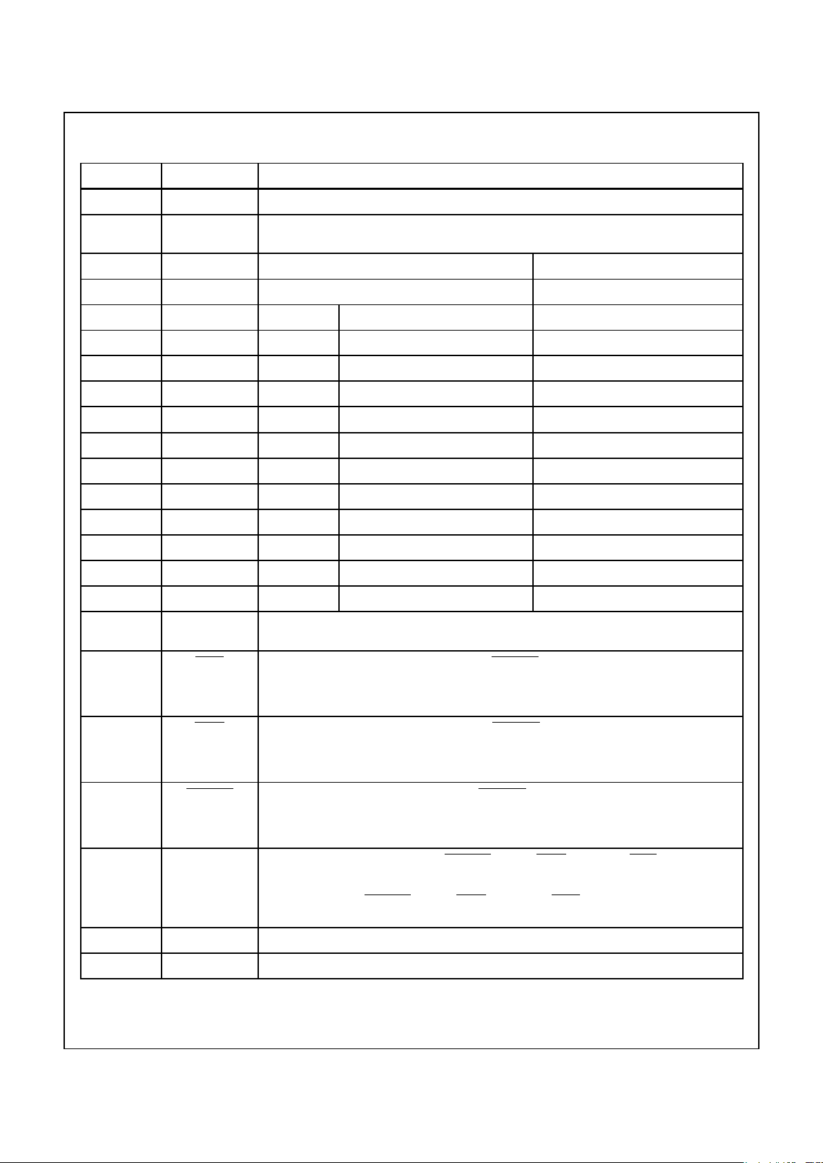
Direct Mode
When the MODE pin is left at a low level, the data outputs
(bits 1 through 8 low order byte, bits 9 through 12, polarity and
over-range high order byte) are accessible under control of
the byte and chip enable terminals as inputs. These three
inputs are all active low, and are provided with pullup resistors
to ensure an inactive high level when left open. When the chip
enable input is low, taking a byte enable input low will allow
the outputs of that byte to become active (three-stated on).
This allows a variety of parallel data accessing techniques to
be used, as shown in the section entitled “Interfacing.” The
timing requirements for these outputs are shown in Figure 6
and Table 1.
It should be noted that these control inputs are
asynchronous with respect to the converter clock - the data
may be accessed at any time. Thus it is possible to access
the latches while they are being updated, which could lead to
erroneous data. Synchronizing the access of the latches with
the conversion cycle by monitoring the STATUS output will
prevent this. Data is never updated while STATUS is low.
FIGURE 5. RUN/HOLD OPERATION
INT
PHASE II
STATIC IN
HOLD STATE
7 COUNTS
AUTOZERO
PHASE I
MIN 1790 COUNTS
MAX 2041 COUNTS
DEINT TERMINATED
AT ZERO CROSSING
DETECTION
INTERNAL
CLOCK
INTERNAL
LATCH
STATUS
OUTPUT
RUN/HOLD
INPUT
INTEGRATOR
OUTPUT
TABLE 1. DIRECT MODE TIMING REQUIREMENTS
(See Note 4 of Electrical Specifications)
DESCRIPTION SYMBOL MIN TYP MAX UNITS
Byte Enable
Width
t
BEA
350 220 - ns
Data Access
Time from Byte
Enable
t
DAB
-210350 ns
Data Hold Time
from Byte
Enable
t
DHB
-150300 ns
Chip Enable
Width
t
CEA
400 260 - ns
Data Access
Time from Chip
Enable
t
DAC
-260400 ns
Data Hold Time
from Chip
Enable
t
DHC
-240400 ns
ICL7109

14
Handshake Mode
The handshake output mode is provided as an alternative
means of interfacing the ICL7109 to digital systems where the
A/D converter becomes active in controlling the flow of data
instead of passively responding to chip and byte enable
inputs. This mode is specifically designed to allow a direct
interface between the ICL7109 and industry-standard UARTs
(such as the Intersil IM6402/3) with no external logic required.
When triggered into the handshake mode, the ICL7109 provides all the control and flag signals necessary to sequentially
transfer two bytes of data into the UART and initiate their
transmission in serial form. This greatly eases the task and
reduces the cost of designing remote data acquisition stations
using serial data transmission.
Entry into the handshake mode is controlled by the MODE pin.
When the MODE terminal is held high, the ICL7109 will enter
the handshake mode after new data has been stored in the output latches at the end of a conversion (See Figures 7 and 8).
The MODE terminal may also be used to trigger entry into the
handshake mode on demand. At any time during the conversion cycle, the low to high transition of a short pulse at the
MODE input will cause immediate entry into the handshake
mode. If this pulse occurs while new data is being stored, the
entry into handshake mode is delayed until the data is stable.
While the converter is in the handshake mode, the MODE input
is ignored, and although conversions will still be performed,
data updating will be inhibited (See Figure 9) until the converter
completes the output cycle and clears the handshake mode.
When the converter enters the handshake mode, or when the
MODE input is high, the chip and byte enable terminals
become TTL-compatible outputs which provide the control
signals for the output cycle (See Figures 7, 8, and 9).
In handshake mode, the SEND input is used by the converter
as an indication of the ability of the receiving device (such as a
UART) to accept data.
Figure 7 shows the sequence of the output cycle with SEND
held high. The handshake mode (Internal MODE high) is
entered after the data latch pulse, and since MODE remains
high the CE/LOAD
, LBEN and HBEN terminals are active as
outputs. The high level at the SEND input is sensed on the
same high to low internal clock edge that terminates the data
latch pulse. On the next low to high internal clock edge the
CE/LOAD
and the HBEN outputs assume a low level, and the
high-order byte (Bits 9 through 12, POL, and OR) outputs are
enabled. The CE/LOAD
output remains low for one full internal
clock period only, the data outputs remain active for 1
1
/2 internal clock periods, and the high byte enable remains low for two
clock periods. Thus the CE/LOAD
output low level or low to
high edge may be used as a synchronizing signal to ensure
valid data, and the byte enable as an output may be used as a
byte identification flag. With SEND remaining high the converter
completes the output cycle using CE/LOAD
and LBEN while
the low order byte outputs (bits 1 through 8) are activated. The
handshake mode is terminated when both bytes are sent.
Figure 8 shows an output sequence where the SEND input is
used to delay portions of the sequence, or handshake to ensure
correct data transfer. This timing diagram shows the relationships that occur using an industry-standard IM6402/3 CMOS
UART to interface to serial data channels. In this interface, the
SEND input to the ICL7109 is driven by the TBRE (Transmitter
Buffer Register Empty) output of the UART, and the CE/LOAD
terminal of the ICL7109 drives the TBRL (Transmitter Buffer
Register Load) input to the UART. The data outputs are paralleled into the eight Transmitter Buffer Register inputs.
FIGURE 6. DIRECT MODE OUTPUT TIMING
TABLE 1. DIRECT MODE TIMING REQUIREMENTS
(See Note 4 of Electrical Specifications)
DESCRIPTION SYMBOL MIN TYP MAX UNITS
DATA
VALID
DATA
VALID
DATA
VALID
t
CEA
t
BEA
t
DAB
t
DHB
t
DAC
t
DHC
CE/LOAD
AS INPUT
HBEN
AS INPUT
LBEN
AS INPUT
HIGH BYTE
DATA
LOW BYTE
DATA
= HIGH IMPEDANCE
ICL7109

15
Assuming the UART Transmitter Buffer Register is empty, the
SEND input will be high when the handshake mode is entered
after new data is stored. The CE/LOAD and HBEN terminals will
go low after SEND is sensed, and the high order byte outputs
become active. When CE/LOAD goes high at the end of one
clock period, the high order byte data is clocked into the UART
Transmitter Buffer Register. The UART TBRE output will now go
low, which halts the output cycle with the HBEN output low, and
the high order byte outputs active. When the UART has transferred that data to the Transmitter Register and cleared the
Transmitter Buffer Register, the TBRE returns high. On the next
ICL7109 internal clock high to low edge, the high order byte outputs are disabled, and one-half internal clock later, the HBEN
output returns high. At the same time, the CE/LOAD and LBEN
outputs go low, and the low order byte outputs become active.
Similarly, when the CE/LOAD returns high at the end of one
clock period, the low order data is clocked into the UART Transmitter Buffer Register, and TBRE again goes low. When TBRE
returns to a high it will be sensed on the next ICL7109 internal
clock high to low edge, disabling the data outputs. One-half
internal clock later, the handshake mode will be cleared, and the
CE/LOAD, HBEN and LBEN terminals return high and stay
inactive (as long as MODE stays high).
With the MODE input remaining high as in these examples,
the converter will output the results of every conversion
except those completed during a handshake operation. By
triggering the converter into handshake mode with a low to
high edge on the MODE input, handshake output
sequences may be performed on demand. Figure 9 shows
a handshake output sequence triggered by such an edge.
In addition, the SEND input is shown as being low when the
converter enters handshake mode. In this case, the whole
output sequence for the first (high order) byte is similar to
the sequence for the second byte. This diagram also shows
the output sequence taking longer than a conversion cycle.
Note that the converter still makes conversions, with the
STATUS output and RUN/HOLD input functioning normally. The only difference is that new data will not be
latched when in handshake mode, and is therefore lost.
Oscillator
The ICL7109 is provided with a versatile three terminal
oscillator to generate the internal clock. The oscillator may be
overdriven, or may be operated with an RC network or crystal.
The OSCILLATOR SELECT input changes the internal configuration of the oscillator to optimize it for RC or crystal operation.
When the OSCILLATOR SELECT input is high or left open
(the input is provided with a pullup resistor), the oscillator is
configured for RC operation, and the internal clock will be of
the same frequency and phase as the signal at the
BUFFERED OSCILLATOR OUTPUT. The resistor and
capacitor should be connected as in Figure 10. The circuit will
oscillate at a frequency given by f = 0.45/RC. A 100kΩ resistor
is recommended for useful ranges of frequency. For optimum
60Hz line rejection, the capacitor value should be chosen
INTEGRATOR
OUTPUT
INTERNAL
CLOCK
INTERNAL
LATCH
STATUS
OUTPUT
MODE
INTERNAL
MODE
SEND
INPUT
CE/LOAD
HBEN
HIGH BYTE
DATA
LBEN
LOW BYTE
DATA
= DON’T CARE
INPUT
ZERO CROSSING
OCCURS
ZERO CROSSING
DETECTED
MODE HIGH ACTIVATES
CE/LOAD
, HBEN, LBEN
UART
NORM
SEND
SENSED
SEND
SENSED
TERMINATES
UART MODE
= THREE-STATE HIGH IMPEDA NCE = THR EE-STATE WITH PULLUP
MODE LOW, NOT
IN HANDSHAKE MODE
DISABLES OUTPUTS CE/LOAD
, HBEN, LBEN
DATA VALID
DATA VALID
FIGURE 7. HANDSHAKE WITH SEND HELD HIGH
ICL7109

16
such that 2048 clock periods is close to an integral multiple of the 60Hz period (but should not be less than 50pF).
When the OSCILLATOR SELECT input is low a feedback
device and output and input capacitors are added to the oscillator. In this configuration, as shown in Figure 11, the oscillator will operate with most crystals in the 1MHz to 5MHz range
with no external components. Taking the OSCILLATOR
SELECT input low also inserts a fixed ÷58 divider circuit
between the BUFFERED OSCILLATOR OUTPUT and the
internal clock. Using an inexpensive 3.58MHz TV crystal, this
division ratio provides an integration time given by:
t
INT
= (2048 clock periods) x (t
CLOCK
) = 33.18ms where:
This time is very close to two 60Hz periods or 33ms. The
error is less than one percent, which will give better than
40dB 60Hz rejection. The converter will operate reliably at
conversion rates of up to 30 per second, which corresponds
to a clock frequency of 245.8kHz.
If at any time the oscillator is to be overdriven, the overdriving signal should be applied at the OSCILLATOR INPUT,
and the OSCILLATOR OUTPUT should be left open. The
internal clock will be of the same frequency, duty cycle, and
phase as the input signal when OSCILLATOR SELECT is
left open. When OSCILLATOR SELECT is at GND, the clock
will be a factor of 58 below the input frequency.
When using the ICL7109 with the IM6403 UART, it is
possible to use one 3.58MHz crystal for both devices. The
BUFFERED OSCILLATOR OUTPUT of the ICL7109 may be
used to drive the OSCILLATOR INPUT of the UART, saving
the need for a second crystal. However, the BUFFERED
OSCILLATOR OUTPUT does not have a great deal of drive
capability, and when driving more than one slave device
external buffering should be used.
Test Input
When the TEST input is taken to a level halfway between V+
and GND, the counter output latches are enabled, allowing
the counter contents to be examined anytime.
When the RUN/HOLD
is low and the TEST input is
connected to GND, the counter outputs are all forced into the
high state, and the internal clock is disabled. When the
RUN/HOLD
returns high and the TEST input returns to the
1
/2 (V+ - GND) voltage (or to V+) and one clock is applied,
all the counter outputs will be clocked to the low state. This
allows easy testing of the counter and its outputs.
ZERO CROSSING
OCCURS
ZERO CROSSING
DETECTED
INTEGRATOR
OUTPUT
INTERNAL
CLOCK
INTERNAL
LATCH
STATUS
OUTPUT
MODE
INPUT
INTERNAL
MODE
UART
NORM
SEND INPUT
(UART TBRE)
CE/LOAD
OUTPUT
(UART TBRL)
HBEN
HIGH BYTE
DATA
LBEN
LOW BYTE
DATA
= DON’T CARE = THREE-STATE HIGH IMPEDANCE
SEND
SENSED
SEND
SENSED
TERMINATES
UART MODE
DATA VALID
DATA VALID
FIGURE 8. HANDSHAKE - TYPICAL UART INTERFACE TIMING
t
CLOCK
58
3.58MHZ
--------------------------=
ICL7109

17
FIGURE 10. RC OSCILLATOR FIGURE 11. CRYSTAL OSCILLATOR
ZERO CROSSING
OCCURS
ZERO CROSSING
DETECTED
INTERNAL
CLOCK
INTERNAL
LATCH
STATUS
OUTPUT
MODE
INPUT
INTERNAL
MODE
UART
NORM
SEND INPUT
CE/LOAD
OUTPUT
HBEN
HIGH BYTE
DATA
LBEN
LOW BYTE
DATA
= DON’T CARE = THREE-STATE HIGH IMPEDANCE
SEND
SENSED
SEND
SENSED
TERMINATES
UART MODE
DATA VALID
DATA VALID
= THREE- STATE WITH PULLUP
SEND
SENSED
LATCH PULSE INHIBITED
IN UART MODE
DEINT
PHASE III
STATUS OUTPUT
UNCHANGED IN
UART MODE
POSITVE TRANSITION CAUSES
ENTRY INTO
UART MODE
FIGURE 9. HANDSHAKE TRIGGERED BY MODE
25
OSC
SEL
BUFFERED
OSC
OUT
V+ OR OPEN
R
C
ƒ
OSC
= 0.45/RC
OSC
IN
OSC
OUT
232224
25
OSC
SEL
BUFFERED
OSC
OUT
GND
CRYSTAL
OSC
IN
OSC
OUT
232224
÷58
V+
CLOCK
ICL7109

18
FIGURE 12. DIRECT MODE CHIP AND BYTE ENABLE COMBINATIONS
FIGURE 13. THREE-STATE SEVERAL ICL7109’S TO A SMALL BUS
GND
MODE
LBEN
B9 - B12
POL, OR
B1 - B8
RUN/HOLD
HBEN
CONVERT
ANALOG
IN
CONTROL
6
8
ICL7109
GND
MODE
LBEN
B1 - B12
POL, OR
RUN/HOLD
HBEN
CONVERT
ANALOG
IN
14
ICL7109
GND
MODE
LBEN
B9 - B12
POL, OR
B1 - B8
RUN/HOLD
HBEN
CONVERT
ANALOG
IN
BYTE FLAGS
6
8
ICL7109
CE/LOAD CE/LOADCE/LOAD
CHIP SELECT 1
GND OR
CHIP SELECT 2
CHIP SELECT
FIGURE 12A.
FIGURE 12B.
FIGURE 12C.
GND
CE/LOAD
LBEN
B9 - B12
POL, OR
B1 - B8
HBEN
ANALOG
IN
6
8
MODE
RUN/HOLD
+5V
CONVERTER
SELECT
8-BIT BUS
GND
CE/LOAD
LBEN
B9 - B12
POL, OR
B1 - B8
HBEN
ANALOG
IN
6
8
MODE
RUN/HOLD
+5V
CONVERTER
SELECT
GND
CE/LOAD
LBEN
B9 - B12
POL, OR
B1 - B8
HBEN
ANALOG
IN
6
8
MODE
RUN/HOLD
+5V
CONVERTER
SELECT
ICL7109 ICL7109 ICL7109
BYTE SELECT FLAGS
ICL7109

19
FIGURE 14. FULL-TIME PARALLEL INTERFACE TO 8040/80/85 MICROPROCESSORS
FIGURE 15. FULL-TIME PARALLEL INTERFACE TO 8048/80/85 MICROPROCESSORS WITH INTERRUPT
GND
MODE
LBEN
B9 - B12
POL, OR
B1 - B8
STATUS
HBEN
SEE TEXT
ANALOG
IN
6
8
ICL7109
CE/LOAD
RUN/HOLD +5 V
GND
ADDRESS BUS
CONTROL BUS
RD WR
PA5 - PA
0
PB7 - PB
0
PC
5
D7 - D0 A0 - A1
CS
8255
(MODE 0)
8008, 8080
8085, 8048, ETC.
DATA BUS
GND
MODE
LBEN
B9 - B12
POL, OR
B1 - B8
STATUS
HBEN
+5V
ANALOG
IN
6
8
ICL7109
CE/LOAD
RUN/HOLD
GND
ADDRESS BUS
CONTROL BUS
RD WR
PA5 - PA
0
PB7 - PB
0
PC
4
D7 - D0 A0 - A1
CS
8255
8008, 8080
8085, 8048, ETC.
PC
6
SEE TEXT
STB
A
1µF
10kΩ
PC
6
INTR
A
INTR
DATA BUS
ICL7109

20
Test Circuit
Typical Applications
Direct Mode Interfacing
Figure 12 shows some of the combinations of chip enable
and byte enable control signals which may be used when
interfacing the ICL7109 to parallel data lines. The CE/LOAD
input may be tied low, allowing either byte to be controlled by
its own enable as in Figure 12A. Figure 12B shows a configuration where the two byte enables are connected together.
In this configuration, the CE/LOAD
serves as a chip enable,
and the HBEN
and LBEN may be connected to GND or
serve as a second chip enable. The 14 data outputs will all
be enabled simultaneously. Figure 12C shows the HBEN
and LBEN as flag inputs, and CE/LOAD as a master enable,
which could be the READ strobe available from most microprocessors.
Figure 13 shows an approach to interfacing several
ICL7109s to a bus, connecting the HBEN
and LBEN signals
of several converters together, and using the CE/LOAD
inputs (perhaps decode from an address) to select the
desired converter.
Some practical circuits utilizing the parallel three-state output
capabilities of the ICL7109 are shown in Figures 14 through
19. Figure 14 shows a straightforward application to the Intel
8048/80/85 microprocessors via an 8255PPI, where the
ICL7109 data outputs are active at all times. The I/O ports of
an 8155 may be used in the same way. This interface can be
used in a read-anytime mode, although a read performed
while the data latches are being updated will lead to
scrambled data. This will occur very rarely, in the proportion of
set-up skew times to conversion time. One way to overcome
this is to read the STATUS output as well, and if it is high, read
the data again after a delay of more than
1
/2 converter clock
period. If STATUS is now low, the second reading is correct,
and if it is still high, the first reading is correct. Alternatively,
this timing problem is completely avoided by using a readafter-update sequence, as shown in Figure 15. Here the high
to low transition of the STATUS output drives an interrupt to
the microprocessor causing it to access the data latches. This
application also shows the RUN/HOLD
input being used to ini-
tiate conversions under software control.
A similar interface to Motorola MC6800 or Rockwell R650X
systems is shown in Figure 16. The high to low transition of
the STATUS output generates an interrupt via the Control
Register B CB1 line. Note that CB2 controls the RUN/HOLD
pin through Control Register B, allowing software-controlled
initiation of conversions in this system as well.
The three-state output capability of the ICL7109 allows direct
interfacing to most microprocessor busses. Examples of this
are shown in Figures 17 and 18. It is necessary to carefully
consider the system in this type of interface, to be sure that
requirements for setup and hold times, and minimum pulse
widths are met. Note also the drive limitations on long buses.
Generally this type of interface is only favored if the memory
peripheral address density is low so that simple address
decoding can be used. Interrupt handling can also require
many additional components, and using an interface device
will usually simplify the system in this case.
13
1
2
3
4
5
6
7
8
9
10
11
12
14
15
16
17
18
19
20
GND
STATUS
POL
OR
B12
B11
B10
B9
B8
B7
B6
B5
B4
B3
B2
B1
TEST
LBEN
HBEN
CE/LOAD
28
40
39
38
37
36
35
34
33
32
31
30
29
27
26
25
24
23
22
21
V+
REF IN -
REF CAP-
REF CAP+
REF IN+
IN HI
IN LO
COMMON
INT
AZ
BUF
REF OUT
V-
SEND
RUN/HOLD
BUF OSC OUT
OSC SEL
OSC OUT
OSC IN
MODE
GND
HIGH
ORDER
BYTE
OUTPUTS
LOW
ORDER
BYTE
OUTPUTS
+5V
BYTE
CONTROL
INPUTS
GND
V+
+5V
1µF
0.01µF
0.33µF
0.15µF
C
AZ
C
INT
R
INT
†
1MΩ R1
1kΩ
24kΩ
3.5795MHz
TV CRYSTAL
†R
INT
= 20kΩ FOR 0.2V REF
= 200kΩ FOR 2.0V REF
REF IN +
REF IN -
-
+
INPUT HIGH
INPU T LOW
GND
DIFFERENTIAL
REFERENCE
-5V
ICL7109

21
Handshake Mode Interfacing
The handshake mode allows ready interface with a wide
variety of external devices. For instance, external latches
may be clocked by the rising edge of CE/LOAD
, and the byte
enables may be used as byte identification flags or as load
enables.
Figure 19 shows a handshake interface to Intel microprocessors again using an 8255PPI. The handshake operation with
the 8255 is controlled by inverting its Input Buffer Full (IBF)
flag to drive the SEND input to the ICL7109, and using the
CE/LOAD
to drive the 8255 strobe. The internal control register of the PPI should be sent in MODE 1 for the port used.
If the ICL7109 is in handshake mode and the 8255 IBF flag
is low, the next word will be strobed into the port. The strobe
will cause IBF to go high (SEND goes low), which will keep
the enable byte outputs active. The PPI will generate an
interrupt which when executed will result in the data being
read. When the byte is read, the IBF will be reset low, which
causes the ICL7109 to sequence into the next byte. This figure shows the MODE input to the ICL7109 connected to a
control line on the PPI. If this output is left high, or tied high
separately, the data from every conversion (provided the
data access takes less time than a conversion) will be
sequenced in two bytes into the system.
If this output is made to go from low to high, the output
sequence can be obtained on demand, and the interrupt
may be used to reset the MODE bit. Note that the
RUN/HOLD
input to the ICL7109 may also be obtained on
command under software control. Note that one port of the
8255 is not used, and can service another peripheral device.
the same arrangement can also be used with the 8155.
Figure 20 shows a similar arrangement with the MC6800 or
MCS650X microprocessors, except that both MODE and
RUN/HOLD
are tied high to save port outputs.
The handshake mode is particularly convenient for directly
interfacing to industry standard UARTs (such as the Intersil
IM6402 or Western Digital TR1602) providing a minimum
component count means of serially transmitting converted
data. A typical UART connection is shown in Figure 1A. In
this circuit, any word received by the UART causes the
UART DR (Data Ready) output to go high. This drives the
MODE input to the ICL7109 high, triggering the ICL7109 into
handshake mode. The high order byte is output to the UART
first, and when the UART has transferred the data to the
Transmitter Register, TBRE (SEND) goes high again, LBEN
will go high, driving the UART DRR (Data Ready Reset)
which will signal the end of the transfer of data from the
ICL7109 to the UART.
Figure 21 shows an extension of the one converter one
UART scheme to several ICL7109s with one UART. In this
circuit, the word received by the UART (available at the RBR
outputs when DR is high) is used to select which converter
will handshake with the UART. With no external components, this scheme will allow up to eight ICL7109s to interface with one UART. Using a few more components to
decode the received word will allow up to 256 converters to
be accessed on one serial line.
MC6820
GND
MODE
ICL7109
B9 - B12
POL, OR
B1 - B8
STATUS
RUN/HOLD
LBENHBENLOAD
CE/
GND
ANALOG
IN
PA0 - 5
PB0 - 7
CB1
CB2
CRB - - 11R-01
MC680X
OR
MCS650X
ADDRESS
BUS
DATA
BUS
CONTROL
BUS
6
8
FIGURE 16. FULL-TIME PARALLEL INTERFACE TO MC680X OR MCS650X MICROPROCESSORS
ICL7109
22
The applications of the ICL7109 are not limited to those
shown here. The purposes of these examples are to provide a starting point for users to develop useful systems
and to show some of the variety of interfaces and uses of
the combination. In particular the uses of the STATUS,
RUN/HOLD
, and MODE signals may be mixed.
The following application notes contain very useful
information on understanding and applying this part and
are available from Intersil Corporation.
Application Notes
NOTE # DESCRIPTION
AnswerFAX
DOC. #
AN016 “Selecting A/D Converters” 9016
AN017 “The Integrating A/D Converter” 9017
AN018 “Do’s and Don’ts of Applying A/D
Converters”
9018
AN030 “The ICL7104 - A Binary Output A/D
Converter for Microprocessors”
9030
AN032 “Understanding the Auto-Zero and
Common Mode Performance of the
ICL7136/7/9 Family”
9032
FIGURE 17. DIRECT INTERFACE - ICL7109 TO 8080/8085
MODE
ICL7109
B9 - B12
B1 - B8
RUN/HOLD
LBENHBEN
GND
ANALOG
IN
+5V
POL, OR
6
8
CE/LOAD
A14 A15
ADDRESS BUS
CONTROL BUS
RD
†
DATA BUS
8008, 8080, 8085
† MEMR OR IOR
FOR 8080/8228 SYSTEM
ICL7109

23
FIGURE 18. DIRECT ICL7109 - MC680X BUS INTERFACE
FIGURE 19. HANDSHAKE INTERFACE - ICL7109 TO 8048, 80/85
74C42
74C30
MC680X
OR
MCS650X
CONTROL
BUS
DATA
BUS
ADDRESS
BUS
A0 - A2
A15 - A10
R/W
, VMA
CE/LOAD
MODE RUN/HOLD
B9 - B12
POL, OR
B1 - B8
HBEN
LBEN
ANALOG
IN
6
8
GND +5V
ANALOG
IN
6
8
STB
A
IBF
A
B9 - B12
POL, OR
ICL7109
B1 - B8
SEND
RUN/HOLD
MODE
CE/LOAD
RD WR D7 - D0 A0 - A1
CS
8255
(MODE 1)
PC
4
PC
5
PC
6
PC
7
PA7 - PA
0
PC
3
ADDRESS BUS
CONTROL BUS
DATA BUS
INTR
8008, 8080,
8085, 8048, ETC.
ICL7109

24
FIGURE 20. HANDSHAKE INTERFACE - ICL7109 TO MC6800, MCS650X
FIGURE 21. MULTIPLEXING CONVERTERS WITH MODE INPUT
ANALOG
IN
HBEN
ICL7109
LBEN
SEND
RUN/HOLD
MODE
CE/LOAD
CRA
MC6820
CA1
CA2
PA
0
- PA
7
- -100 - 01
MC6800
OR
MCS650X
ADDRESS
BUS
DATA
BUS
CONTROL
BUS
+5V
MODE SENDCE/
LOAD
B9 - B12
POL, OR
SEND
RUN/HOLD
HBEN LBEN
ANALOG
IN
+5V
MODE SENDCE/
LOAD
B9 - B12
POL, OR
SEND
RUN/HOLD
HBEN LBEN
ANALOG
IN
+5V
MODE SENDCE/
LOAD
B9 - B12
POL, OR
SEND
HBEN
LBEN
ANALOG
IN
6
8
6
8
6
8
TBRL DRR TBRE RBR1 - RBR8 TBR1 - TBR8
SERIAL INPUT
SERIAL OUTPUT
IM6402 CMOS UART
23
8-BIT DATA BUS
RUN/HOLD +5V

25
Die Characteristics
DIE DIMENSIONS:
(122 mils x 135 mils) x 525µm ±25µm Thick
METALLIZATION:
Type: Al
Thickness: 10k
Å ±1kÅ
PASSIVATION:
Type: Nitride/Silox Sandwich
Thickness: 8k
Å Nitride over 7kÅ Silox
Metallization Mask Layout
ICL7109
B1 B2 B3 B4 B5 B6 B7 B8 B9 B10 B11 B12
OR
POL
STATUS
GND
REF IN-
REF CAP-
REF CAP+
REF IN+
IN HIIN LOCOMMONINTAZBUFREF OUTSEND V-RUN/HOLD
TEST
LBEN
HBEN
CE/LOAD
MODE
OSC IN
OSC OUT
OSC SEL
BUF OSC OUT
V+
 Loading...