

May 2002
www.BDTIC.com/Intersil
®
HM-65642/883
8K x 8 Asynchronous
CMOS Static RAM
Features
• This Circuit is Processed in Accordance to MIL-STD883 and is Fully Conformant Under the Provisions of
Paragraph 1.2.1.
• Full CMOS Design
• Six Transistor Memory Cell
• Low Standby Supply Current . . . . . . . . . . . . . . . .100µA
• Low Operating Supply Current. . . . . . . . . . . . . . . 20mA
• Fast Address Access Time. . . . . . . . . . . . . . . . . . 150ns
• Low Data Retention Supply Voltage . . . . . . . . . . . 2.0V
• CMOS/TTL Compatible Inputs/Outputs
• JEDEC Approved Pinout
• Equal Cycle and Access Times
• No Clocks or Strobes Required
Description
The HM-65642/883 is a CMOS 8192 x 8-bit Static Random
Access Memory. The pinout is the JEDEC 28 pin, 8-bit wide
standard, which allows easy memory board layouts which
accommodate a variety of industry standard ROM, PROM,
EPROM, EEPROM and RAMs. The HM-65642/883 is ideally
suited for use in microprocessor based systems. In particular, interfacing with the Intersil 80C86 and 80C88 microprocessors is simplified by the convenient output enable (G
input.
The HM-65642/883 is a full CMOS RAM which utilizes an
array of six transistor (6T) memory cells for the most stable
and lowest possible standby supply current over the full military temperature range.
• Gated Inputs
- No Pull-Up or Pull-Down Resistors Required
• Temperature Range -55
o
C to +125oC
• Easy Microprocessor Interfacing
• Dual Chip Enable Control
Ordering Information
PACKAGE TEMPERATURE RANGE 150ns/75µA 150ns/150µA 200ns/250µA PKG. NO.
o
CERDIP -55
CLCC -55
C to +125oC HM1-65642B/883 HM1-65642/883 HM1-65642C/883 F28.6
o
C to +125oC HM4-65642B/883 HM4-65642/883 - J32.A
)
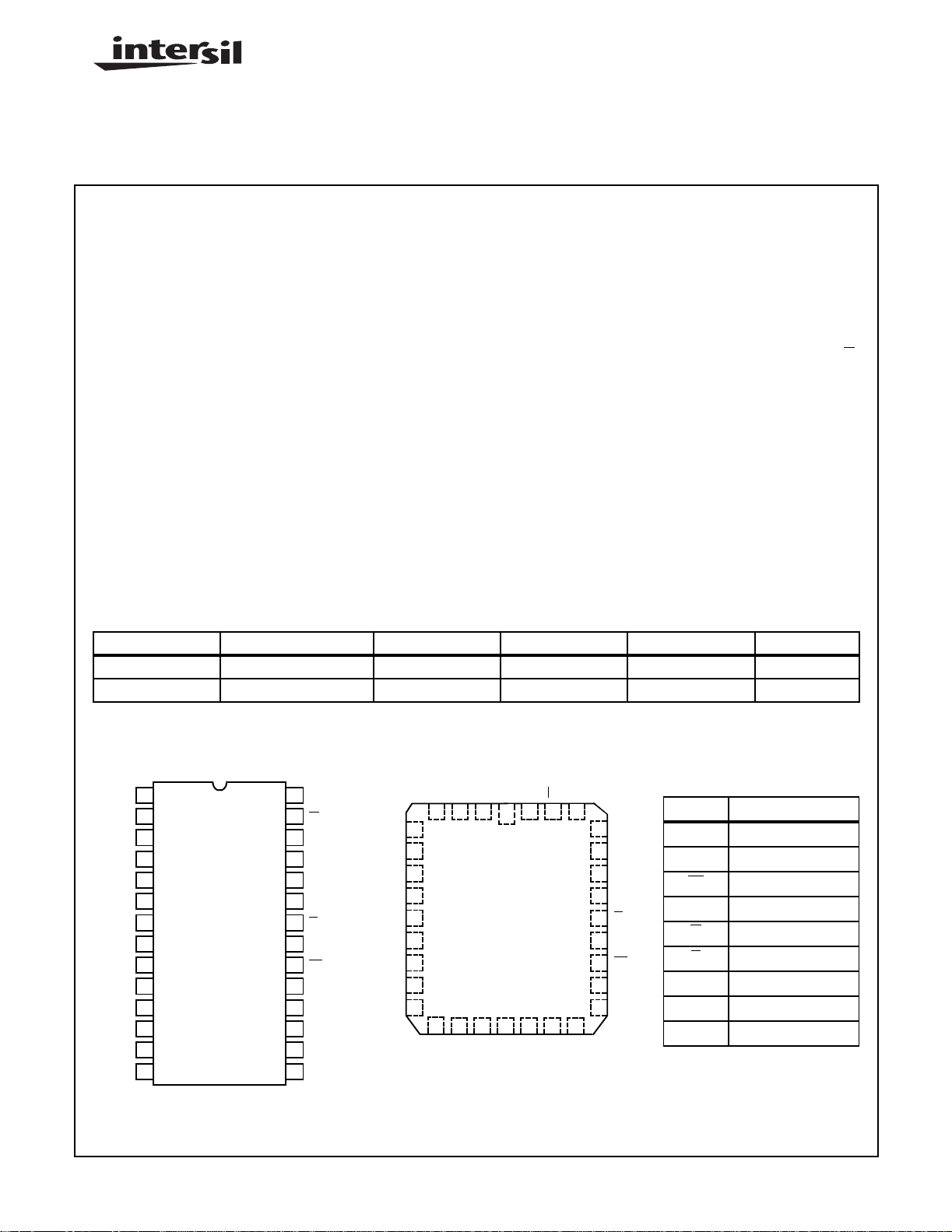
Pinouts
HM-65642/883 (CERDIP)
TOP VIEW
1
NC
2
A12
3
A7
4
A6
5
A5
6
A4
7
A3
8
A2
9
A1
10
A0
11
DQ0
12
DQ1
13
DQ2
14
GND
CAUTION: These devices are sensitive to electrostatic discharge; follow proper IC Handling Procedures.
1-888-INTERSIL or 321-724-7143
28
VCC
27
W
26
E2
25
A8
24
A9
23
A11
22
G
21
A10
20
E1
19
DQ7
18
DQ6
17
DQ5
16
DQ4
15
DQ3
| Intersil (and design) is a registered trademark of Intersil Americas Inc.
Copyright © Intersil Americas Inc. 2002. All Rights Reserved
A6
A5
A4
A3
A2
A1
A0
NC
DQ0
HM4-65642/883 (CLCC)
TOP VIEW
NC
A7
4 32 31 30
5
6
7
8
9
10
11
12
13
14
DQ1
NC
A12
1
3 2
16 17 18 19 20
15
NC
DQ2
GND
220
VCC
DQ3
E2
W
29
A8
28
A9
27
A11
26
NC
25
G
24
A10
23
E1
22
DQ7
21
DQ6
DQ4
DQ5
PIN DESCRIPTION
A Address Input
DQ Data Input/Output
E1
E2 Chip Enable
NC No Connections
GND Ground
VCC Power
W
G
Chip Enable
Write Enable
Output Enable
FN3004.2
HM-65642/883
www.BDTIC.com/Intersil
Absolute Maximum Ratings Thermal Information
Supply Voltage . . . . . . . . . . . . . . . . . . . . . . . . . . . . . . . . . . . . . +7.0V
Input or Output Voltage Applied for all Grades. . . . . . . GND -0.3V to
VCC +0.3V
Typical Derating Factor . . . . . . . . . . . 5mA/MHz Increase in ICCOP
ESD Classification . . . . . . . . . . . . . . . . . . . . . . . . . . . . . . . . Class 1
Thermal Resistance (Typical) θ
CERDIP Package . . . . . . . . . . . . . . . . 45oC/W 8oC/W
CLCC Package . . . . . . . . . . . . . . . . . . 55
Maximum Storage Temperature Range . . . . . . . . .-65
Maximum Junction Temperature. . . . . . . . . . . . . . . . . . . . . . +175
Maximum Lead Temperature (Soldering 10s). . . . . . . . . . . . +300
JA
o
C/W 10oC/W
Die Characteristics
Gate Count . . . . . . . . . . . . . . . . . . . . . . . . . . . . . . . . 101,000 Gates
CAUTION: Stresses above those listed in “Absolute Maximum Ratings” may cause permanent damage to the device. This is a stress only rating and operation
of the device at these or any other conditions above those indicated in the operational sections of this specification is not implied.
Operating Conditions
Operating Voltage Range. . . . . . . . . . . . . . . . . . . . . +4.5V to +5.5V
Operating Temperature Range. . . . . . . . . . . . . . . . -55
Input Low Voltage. . . . . . . . . . . . . . . . . . . . . . . . . . . . -0.3V to +0.8V
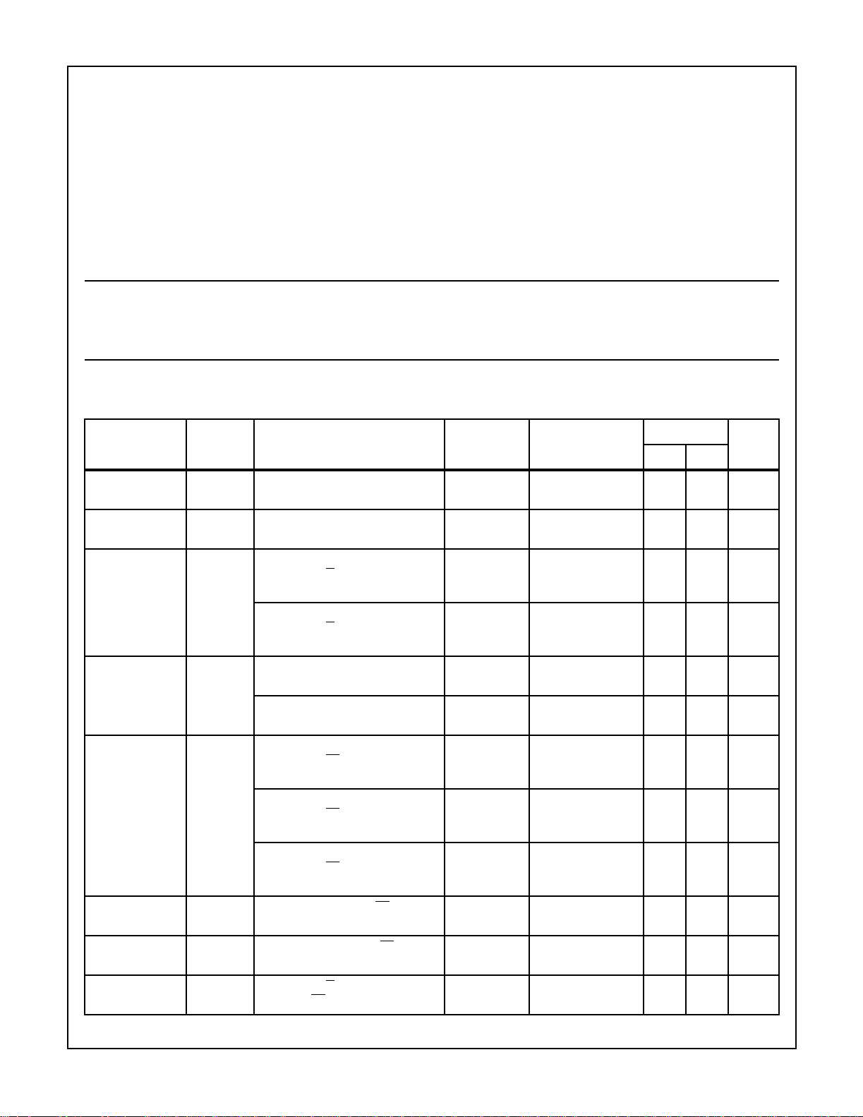
TABLE 1. HM-65642/883 DC ELECTRICAL PERFORMANCE SPECIFICATIONS
Device Guaranteed and 100% Tested
PARAMETER SYMBOL
High Level Output
Voltage
Low Level Output
Voltage
High Impedance
Output Leakage
Current
Input Leakage
Current
Standby Supply
Current
VOH 1 VCC = 4.5V, IO = -1.0mA 1, 2, 3 -55
VOL VCC = 4.5V, IO = 4.0mA 1, 2, 3 -55
IIOZ HM-65642B/883, HM-65642/883
VCC = 5.5V, G
VI/O = GND or VCC
HM-65642C/883
VCC = 5.5V, G
VI/O = GND or VCC
II HM-65642B/883, HM-65642/883
VCC = 5.5V, VI = GND or VCC
HM-65642C/883
VCC = 5.5V, VI = GND or VCC
ICCSB1 HM-65642B/883
VCC = 5.5V, E1
E2 = GND +0.3V
HM-65642/883
VCC = 5.5V, E1
E2 = GND +0.3V
HM-65642C/883
VCC = 5.5V, E1
E2 = GND +0.3V
o
C to +125oC
(NOTE 1)
CONDITIONS
= 2.2V,
= 2.2V,
= VCC -0.3V or
= VCC -0.3V or
= VCC -0.3V or
Input High Voltage. . . . . . . . . . . . . . . . . . . . . . . +2.2V to VCC +0.3V
Data Retention Supply Voltage. . . . . . . . . . . . . . . . . . . . . . . . . 2.0V
Input Rise and Fall Time. . . . . . . . . . . . . . . . . . . . . . . . . . 40ns Max.
GROUP A
SUBGROUPS TEMPERATURE
o
C ≤ TA ≤
o
C
+125
o
C ≤ TA ≤
o
C
+125
o
1, 2, 3 -55
1, 2, 3 -55
1, 2, 3 -55
1, 2, 3 -55
1, 2, 3 -55
1, 2, 3 -55
1, 2, 3 -55
C ≤ TA ≤
o
+125
o
C ≤ TA ≤
o
+125
o
C ≤ TA ≤
o
+125
o
C ≤ TA ≤
o
+125
o
C ≤ TA ≤
o
+125
o
C ≤ TA ≤
o
+125
o
C ≤ TA ≤
o
+125
C
C
C
C
C
C
C
LIMITS
2.4 - V
-0.4 V
-1.0 +1.0 µA
-2.0 +2.0 µA
-1.0 +1.0 µA
-2.0 +2.0 µA
- 100 µA
- 250 µA
- 400 µA
θ
JC
o
C to +150oC
UNITSMIN MAX
o
o
C
C
Standby Supply
Current
Enable Supply
Current
Operating Supply
Current
ICCSB VCC = 5.5V, IO = 0mA, E1
E2 = 0.8V
ICCEN VCC = 5.5V, IO = 0mA, E1
ICCOP VCC = 5.5V, G
E2 = 2.2V
f = 1MHz, E1
= 5.5V, (Note 2),
= 0.8V, E2 = 2.2V
= 2.2V or
=0.8V,
1, 2, 3 -55oC ≤ TA ≤
1, 2, 3 -55oC ≤ TA ≤
1, 2, 3 -55
o
+125
o
+125
o
C ≤ TA ≤
o
+125
C
C
C
221
-5mA
-5mA
-20mA
HM-65642/883
www.BDTIC.com/Intersil
TABLE 1. HM-65642/883 DC ELECTRICAL PERFORMANCE SPECIFICATIONS (Continued)
Device Guaranteed and 100% Tested
PARAMETER SYMBOL
Data Retention
ICCDR HM-65642B/883
Supply Current
VCC = 2.0V, E1
CONDITIONS
= VCC -0.3V or
E2 = GND +0.3V
HM-65642/883
(NOTE 1)
VCC = 2.0V, E1
= VCC -0.3V or
E2 = GND +0.3V
HM-65642C/883
VCC = 2.0V, E1
= VCC -0.3V or
E2 = GND +0.3V
Functional Test FT VCC = 4.5V (Note 3) 7, 8A, 8B -55
NOTES:
1. All voltages referenced to device GND.
2. Typical derating 5mA/MHz increase in ICCOP.
3. Tested as follows: f = 2MHz, VIH = 2.4V, VIL = 0.4V, IOH = -4.0mA, IOL = 4.0mA, VOH ≥ 1.5V, and VOL ≤ 1.5V.
GROUP A
SUBGROUPS TEMPERATURE
o
1, 2, 3 -55
1, 2, 3 -55
1, 2, 3 -55
C ≤ TA ≤
o
+125
o
C ≤ TA ≤
o
+125
o
C ≤ TA ≤
o
+125
o
C ≤ TA ≤
o
+125
C
C
C
C
LIMITS
UNITSMIN MAX
-75µA
- 150 µA
- 250 µA
-- -
PARAMETERS SYMBOL
Read/Write/
Cycle Time
Address Access
Time
Output Enable
Access Time
Chip Enable
Access Time
Write Recovery
Time
Chip Enable to
End-of-Write
Address Setup
Time
Write Enable
Pulse Width
Data Setup Time TDVWH
TAVAX VCC = 4.5V and
TAVQV VCC = 4.5V and
TGLQV VCC = 4.5V and
TE1LQV
TE2HQV
TWHAX
TE1HAX
TE2LAX
TE1LE1H
TE2HE2L
TAVWL
TAVE1L
TAVE2H
TWLWH VCC = 4.5V and
TDVE1H
TDVE2L
TABLE 2. HM-65642/883 AC ELECTRICAL PERFORMANCE SPECIFICATIONS
LIMITS
(NOTES 1, 2)
CONDITIONS
5.5V
5.5V
5.5V
VCC = 4.5V and
5.5V
VCC = 4.5V and
5.5V
VCC = 4.5V and
5.5V
VCC = 4.5V and
5.5V
5.5V
VCC = 4.5V and
5.5V
GROUP A
SUB-
GROUPS TEMPERATURE
o
9, 10, 11 -55
9, 10, 11 -55
9, 10, 11 -55
9, 10, 11 -55
9, 10, 11 -55
9, 10, 11 -55
9, 10, 11 -55
9, 10, 11 -55
9, 10, 11 -55
C ≤ TA ≤ +125oC 150 - 150 - 200 - ns
o
C ≤ TA ≤ +125oC - 150 - 150 - 200 -
o
C ≤ TA ≤ +125oC - 70 - 70 - 70 ns
o
C ≤ TA ≤ +125oC - 150 - 150 - 200 ns
o
C ≤ TA ≤ +125oC10-10-10- ns
o
C ≤ TA ≤ +125oC 90 - 90 - 120 - ns
o
C ≤ TA ≤ +125oC0-0-0-ns
o
C ≤ TA ≤ +125oC 90 - 90 - 120 - ns
o
C ≤ TA ≤ +125oC60-60-80- ns
HM-
65642B/883
MIN MAX MIN MAX MIN MAX
HM-
65642/883
HM-
65642C/883
UNITS
222
HM-65642/883
www.BDTIC.com/Intersil
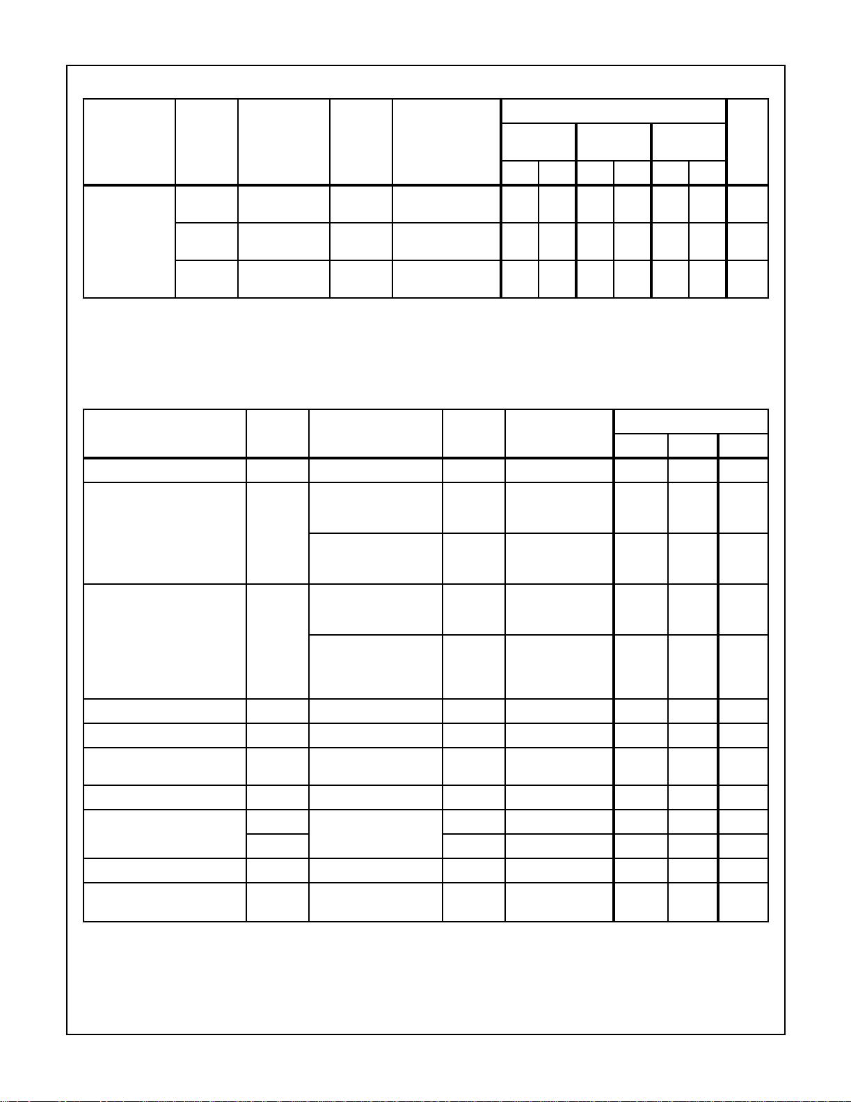
TABLE 2. HM-65642/883 AC ELECTRICAL PERFORMANCE SPECIFICATIONS (Continued)
LIMITS
PARAMETERS SYMBOL
Data Hold Time TWHDX VCC = 4.5V and
TE1HDX VCC = 4.5V and
TE2LDX VCC = 4.5V and
(NOTES 1, 2)
CONDITIONS
5.5V
5.5V
5.5V
GROUP A
SUB-
GROUPS TEMPERATURE
9, 10, 11 -55oC ≤ TA ≤ +125oC5-5-5-ns
9, 10, 11 -55
9, 10, 11 -55
o
C ≤ TA ≤ +125oC10-10-10- ns
o
C ≤ TA ≤ +125oC10-10-10- ns
HM-
65642B/883
MIN MAX MIN MAX MIN MAX
HM-
65642/883
HM-
65642C/883
UNITS
NOTES:
1. All voltages referenced to device GND.
2. AC measurements assume transition time ≤ 5ns; input levels = 0.0V to 3.0V; timing reference levels = 1.5V; output load = 1TTL equivalent
load and CL ≥ 50pF, for CL > 50pF, access times are derated 0.15ns/pF.
TABLE 3. HM-65642/883 ELECTRICAL PERFORMANCE SPECIFICATIONS
LIMITS
PARAMETER SYMBOL CONDITIONS NOTES TEMPERATURE
o
Output High Voltage VOH2 VCC = 4.5V, IO = -100µA1-55
Input Capacitance CIN VCC = Open, f = 1MHz, All
Measurements Referenced to Device Ground
1, 2 T
C ≤ TA ≤ +125oC VCC -0.4 - V
= +25oC - 12 pF
A
MIN MAX UNITS
VCC = Open, f = 1MHz, All
Measurements Referenced to Device Ground
I/O Capacitance CI/O VCC = Open, f = 1MHz, All
Write Enable to Output in High Z TWLQZ VCC = 4.5V and 5.5V 1 -55
Write Enable High to Output ON TWHQX VCC = 4.5V and 5.5V 1 -55
Chip Enable to Output ON TE1LQX
Output Enable to Output ON TGLQX VCC = 4.5V and 5.5V 1 -55
Chip Enable to Output in High Z TE1HQZ VCC = 4.5V and 5.5V 1 -55
Output Disable to Output in High Z TGHQZ VCC = 4.5V and 5.5V 1 -55
Output Hold from Address
TE2HQX
TE2LQZ 1 -55
TAXQX VCC = 4.5V and 5.5V 1 -55oC ≤ TA ≤ +125oC10 - ns
Measurements Referenced to Device Ground
VCC = 4.5V, VI/O = GND
or VCC, All Measurements
Referenced to Device
Ground
VCC = 4.5V and 5.5V 1 -55
1, 3 T
1, 2 T
1, 3 T
o
o
o
o
o
o
o
= +25oC - 10 pF
A
= +25oC - 14 pF
A
= +25oC - 12 pF
A
C ≤ TA ≤ +125oC - 50 ns
C ≤ TA ≤ +125oC5 - ns
C ≤ TA ≤ +125oC10 - ns
C ≤ TA ≤ +125oC5 - ns
C ≤ TA ≤ +125oC - 50 ns
C ≤ TA ≤ +125oC - 60 ns
C ≤ TA ≤ +125oC - 50 ns
Change
NOTES:
1. The parameters listed in Table 3 are controlled via design or process parameters and are not directly tested. These parameters are characterized upon initial design release and upon design changes which would affect these characteristics.
2. Applies to DIP device types only. For design purposes CIN = 6pF typical and CI/O = 7pF typical.
3. Applies to LCC device types only. For design purposes CIN = 4pF typical and CI/O = 5pF typical.
223

HM-65642/883
www.BDTIC.com/Intersil
TABLE 4. APPLICABLE SUBGROUPS
CONFORMANCE GROUPS GROUPS METHOD SUBGROUPS
Interim Test 1 100%/5004 -
Interim Test 100%/5004 1, 7, 9
PDA 100%/5004 1
Final Test 1 100%/5004 2, 3, 8A, 8B, 10, 11
Group A Samples/5005 1, 2, 3, 7, 8A, 8B, 9, 10, 11
Groups C and D Samples/5005 1, 7, 9
224

HM-65642/883
www.BDTIC.com/Intersil
Low Voltage Data Retention
Intersil CMOS RAMs are designed with battery backup in
mind. Data Retention voltage and supply current are guaranteed over the operating temperature range. The following
rules ensure data retention:
DATA RETENTION MODE
VCC
4.5V
VIH
E2
VCCOR
GND
FIGURE 1. DATA RETENTION
Read Cycles
1. The RAM must be kept disabled during data retention. This is accomplished by holding the E2 pin between -0.3V and GND.
2. During power-up and power-down transitions, E2 must be held
between -0.3V and 10% of VCC.
3. The RAM can begin operating one TAVAX after VCC reaches the
minimum operating voltage of 4.5V.
TAVAX
TAVAX
A
Q
ADDRESS 1
TAVQV TAXQX
DATA 1
FIGURE 2. READ CYCLE I: W, E2 HIGH; G, E1 LOW
ADDRESS 2
DATA 2
225

Read Cycles
www.BDTIC.com/Intersil
A
E1
HM-65642/883
TAVAX
TAVQV
E2
TE1LQV
TE1LQX
TE2HQX
G
TGLQV
TGLQX
Q
FIGURE 3. READ CYCLE II: W HIGH
TE1HQZ
TE2LQZTE2HQV
TGHQZ
226

Write Cycles
www.BDTIC.com/Intersil
A
HM-65642/883
TAVAX
E1
E2
TAVWL
W
D
TWLQZ
Q
FIGURE 4. WRITE CYCLE I: LATE WRITE
A
TAVE1L
W
TWLWH TWHAX
TWHQX
TWHDXTDVWH
TAVAX
TE1LE1H
TE1HAX
E1
E2
TDVE1H
D
FIGURE 5. WRITE CYCLE II: EARLY WRITE - CONTROLLED BY E1
TE1HDX
227

Write Cycles
www.BDTIC.com/Intersil
A
HM-65642/883
TAVAX
E1
E2
TAVE2H TE2LAX
W
D
FIGURE 6. WRITE CYCLE III: EARLY WRITE - CONTROLLED BY E2
TE2HE2L
TDVE2L
TE2LDX
All Intersil U.S. products are manufactured, assembled and tested utilizing ISO9000 quality systems.
Intersil Corporation’s quality certifications can be viewed at www.intersil.com/design/quality
Intersil products are sold by description only. Intersil Corporation reserves the right to make changes in circuit design, software and/or specifications at any time without
notice. Accordingly, the reader is cautioned to verify that data sheets are current before placing orders. Information furnished by Intersil is believed to be accurate and
reliable. However, no responsibility is assumed by Intersil or its subsidiaries for its use; nor for any infringements of patents or other rights of third parties which may result
from its use. No license is granted by implication or otherwise under any patent or patent rights of Intersil or its subsidiaries.
For information regarding Intersil Corporation and its products, see www.intersil.com
228

Test Circuit
www.BDTIC.com/Intersil
DUT
NOTE:
1. Test head capacitance.
Burn-In Circuits
NC
1
F15
F10
F9
F8
F7
F6
F5
F4
F3
F2
F2
F2
A12
A7
A6
A5
A4
A3
A2
A1
A0
DQ0
DQ1
DQ2
GND
2
3
4
5
6
7
8
9
10
11
12
13
14
(NOTE 1) C
HM-65642/883
CERDIP
TOP VIEW
L
+
1.5V IOLIOH
-
EQUIVALENT CIRCUIT
HM-65642/883
CLCC
TOP VIEW
VCC
F10
C
GND
VCC
28
W
27
E2
26
A8
25
A9
24
A11
23
G
22
A10
21
E1
20
DQ7
19
DQ6
18
DQ5
17
DQ4
16
DQ3
15
F1
F16
F11
F12
F14
F0
F13
F0
F2
F2
F2
F2
F2
F9
F8
F7
F6
F5
F4
F3
DQ0
A6
A5
A4
A3
A2
A1
A0
NC
5
6
7
8
9
10
11
12
13
F15
A12
A7
4 32 31 30
14 15 16 17 18 19 20
DQ1
3 2
DQ2
NC
1
GND
NC
NC
VCC
DQ3
F1
F16
E2
W
DQ4
DQ5
C
A8
29
A9
28
A11
27
NC
26
G
25
A10
24
E1
23
DQ7
22
DQ6
21
F11
F12
F14
F0
F13
F0
F2
F2
F2F2F2
NOTES:
F0 = 100kHz ±10%.
All resistors 47kΩ ±5%.
C = 0.01µF Min.
VCC = 5.5V ±0.5V.
VIH = 4.5V ±10%.
NOTES:
F0 = 100kHz ±10%.
C = 0.01µF Min.
VCC = 5.5V ±0.5V.
VIH = 4.5V ±10%.
VIL = -0.2V to +0.4V.
VIL = -0.2V to +0.4V.
229
F2
F2
F2

Die Characteristics
www.BDTIC.com/Intersil
DIE DIMENSIONS:
274.0 x 302.8 x 19 ±1mils
METALLIZATION:
Type: Si - Al
Thickness: 11k
Å ±2kÅ
Metallization Mask Layout
A8 A7 A12 VCC W E2 A8
A5
A4
A3
GLASSIVATION:
Type: SiO
Thickness: 8kÅ ±1kÅ
WORST CASE CURRENT DENSITY:
0.9 x 10
HM-65642/883
2
5
A/cm
2
A9
A11
G
A2
A1
A0
DQ6DQ5DQ4DQ3GNDDQ2DQ1DQ0
All Intersil U.S. products are manufactured, assembled and tested utilizing ISO9000 quality systems.
Intersil Corporation’s quality certifications can be viewed at www.intersil.com/design/quality
Intersil products are sold by description only. Intersil Corporation reserves the right to make changes in circuit design, software and/or specifications at any time without
notice. Accordingly, the reader is cautioned to verify that data sheets are current before placing orders. Information furnished by Intersil is believed to be accurate and
reliable. However, no responsibility is assumed by Intersil or its subsidiaries for its use; nor for any infringements of patents or other rights of third parties which may result
from its use. No license is granted by implication or otherwise under any patent or patent rights of Intersil or its subsidiaries.
For information regarding Intersil Corporation and its products, see www.intersil.com
230
A10
E1
DQ7
 Loading...