


HI7106
July 1998
Features
• Guaranteed Zero Reading for 0V Input on All Scales
• True Polarity at Zero for Precise Null Detection
• 1pA Typical Input Current
• True Differential Input and Reference,
Direct Display Drive
• Low Noise - Less Than 15µV
P-P
• On Chip Clock and Reference
• Low Power Dissipation - Typically Less Than 10mW
• No Additional Active Circuits Required
• Enhanced Display Stability
• Enhanced VCOM Reference Stability
Ordering Information
TEMP.
PART NO.
HI7106CPL 0 to 70 40 Ld PDIP E40.6
HI7106CM44 0 to 70 44 Ld MQFP Q44.10x10
HI7106C/D 0 to 70 DIE
RANGE (oC) PACKAGE PKG. NO.
31/2 Digit, LCD/LED Display, A/D Converter
Description
The Intersil HI7106 is a high performance, low power, 31/
digit A/D converter. Included are seven segment decoders,
display drivers, a reference, and a clock. The HI7106 is
designed to interface with a liquid crystal display (LCD) and
includes a multiplexed backplane drive.
The HI7106 brings together a combination of high accuracy,
versatility, and true economy. It features auto-zero to less
than 10µV, zero drift of less than 1µV/
o
C, input bias current
of 10pA (Max), and rollover error of less than one count.
True differential inputs and reference are useful in all systems, but give the designer an uncommon advantage when
measuring load cells, strain gauges and other bridge type
transducers. Finally, the true economy of single power supply
operation enables a high performance panel meter to be built
with the additionof only 10 passive components and a display.
2
Pinouts
(1’s)
(10’s)
(100’s)
(1000) AB4
(MINUS)
V+
D1
C1
B1
A1
F1
G1
E1
D2
C2
B2
A2
F2
E2
D3
B3
F3
E3
POL
1
2
3
4
5
6
7
8
9
10
11
12
13
14
15
16
17
18
19
20
HI7106
(PDIP)
TOP VIEW
40
39
38
37
36
35
34
33
32
31
30
29
28
27
26
25
24
23
22
21
OSC 1
OSC 2
OSC 3
TEST
REF HI
REF LO
+
C
REF
-
C
REF
COMMON
IN HI
IN LO
A-Z
BUFF
INT
VG2 (10’s)
C3
(100’s)
A3
G3
BP/GND
NC
NC
TEST
OSC 3
NC
OSC 2
OSC 1
V+
D1
C1
B1
HI7106
(MQFP)
TOP VIEW
+
-
REF
REF
C
REF HI
REF LO
44 43 42 41 40
1
2
3
4
5
6
7
8
9
10
11
12 13 14 15 16 17
A1 F1 G1 E1 D2 C2
COMMON
C
IN HI
IN LO
A-Z
BUFF
INT
39 38 37 36 35 34
2221201918
B2 A2 F2 E2 D3
V-
33
32
31
30
29
28
27
26
25
24
23
NC
G2
C3
A3
G3
BP/GND
POL
AB4
E3
F3
B3
CAUTION: These devices are sensitive to electrostatic discharge; follow proper IC Handling Procedures.
http://www.intersil.com or 407-727-9207
| Copyright © Intersil Corporation 1999
1
File Number 4551
HI7106
Absolute Maximum Ratings Thermal Information
Supply Voltage
HI7106, V+ to V- . . . . . . . . . . . . . . . . . . . . . . . . . . . . . . . . . . . 15V
Analog Input Voltage (Either Input) (Note 1). . . . . . . . . . . . . V+ to V-
Reference Input Voltage (Either Input) . . . . . . . . . . . . . . . . . V+ to V-
Clock Input
HI7106 . . . . . . . . . . . . . . . . . . . . . . . . . . . . . . . . . . . . TEST to V+
Operating Conditions
Temperature Range . . . . . . . . . . . . . . . . . . . . . . . . . . . .0oC to 70oC
CAUTION: Stresses above those listed in “Absolute Maximum Ratings” may cause permanent damage to the device. This is a stress only rating and operation
of the device at these or any other conditions above those indicated in the operational sections of this specification is not implied.
NOTES:
1. Input voltages may exceed the supply voltages provided the input current is limited to ±100µA.
2. θJA is measured with the component mounted on an evaluation PC board in free air.
Electrical Specifications (Note 3)
PARAMETER TEST CONDITIONS MIN TYP MAX UNIT
SYSTEM PERFORMANCE
Zero Input Reading V
Stability (Last Digit) Fixed Input Voltage (Note 6) -000.1 ±000.0 +000.1 Digital
Ratiometric Reading VlN = V
Rollover Error -V
Linearity Full Scale = 200mV or Full Scale = 2V Maximum
Common Mode Rejection Ratio VCM = 1V, VIN = 0V, Full Scale = 200mV (Note 6) - 50 - µV/V
Noise V
Leakage Current Input V
Zero Reading Drift V
Scale Factor Temperature Coefficient V
End Power Supply Character V+ Supply
Current
COMMON Pin Analog Common Voltage 25kΩ Between Common and
Temperature Coefficient of Analog Common 25kΩ Between Common and
DISPLAY DRIVER
Peak-To-Peak Segment Drive Voltage
Peak-To-Peak Backplane Drive Voltage
NOTES:
3. Dissipation rating assumes device is mounted with all leads soldered to printed circuit board.
4. Unless otherwise noted, specifications apply to both the HI7106 and ICL7107 at T
circuit of Figure 1.
5. Back plane drive is in phase with segment drive for ‘off’ segment, 180 degrees out of phase for ‘on’ segment. Frequency is 20 times
conversion rate. Average DC component is less than 50mV.
6. Not tested, guaranteed by design.
= 0.0V, Full Scale = 200mV -000.0 ±000.0 +000.0 Digital
IN
, V
REF
REF
= +VlN≅ 200mV
IN
Difference in Reading for Equal Positive and
Negative Inputs Near Full Scale
Deviation from Best Straight Line Fit (Note 6)
= 0V, Full Scale = 200mV
IN
(Peak-To-Peak Value Not Exceeded 95% of Time)
= 0 (Note 6) - 1 10 pA
lN
= 0, 0oC To 70oC (Note 6) - 0.2 1 µV/oC
lN
= 199mV, 0oC To 70oC,
IN
(Ext. Ref. 0ppm/oC) (Note 6)
V
= 0 - 0.6 1.8 mA
IN
Positive Supply (With Respect to + Supply)
Positive Supply (With Respect to + Supply)
V+ = to V- = 9V (Note 5) 4 5 6 V
Thermal Resistance (Typical, Note 2) θJA (oC/W)
PDIP Package. . . . . . . . . . . . . . . . . . . . . . . . . . . . . . . 50
MQFP Package. . . . . . . . . . . . . . . . . . . . . . . . . . . . . . 80
Maximum Junction Temperature. . . . . . . . . . . . . . . . . . . . . . . 150oC
Maximum Storage Temperature Range . . . . . . . . . .-65oC to 150oC
Maximum Lead Temperature (Soldering 10s). . . . . . . . . . . . . 300oC
(MQFP - Lead Tips Only)
Reading
Reading
= 100mV 999 999/10001000 Digital
Reading
- ±0.2 ±1 Counts
- ±0.2 ±1 Counts
-15- µV
- 1 5 ppm/oC
2.4 2.8 3.2 V
- 80 - ppm/
=25oC, f
A
CLOCK
= 48kHz. HI7106 is tested in the
o
C
2
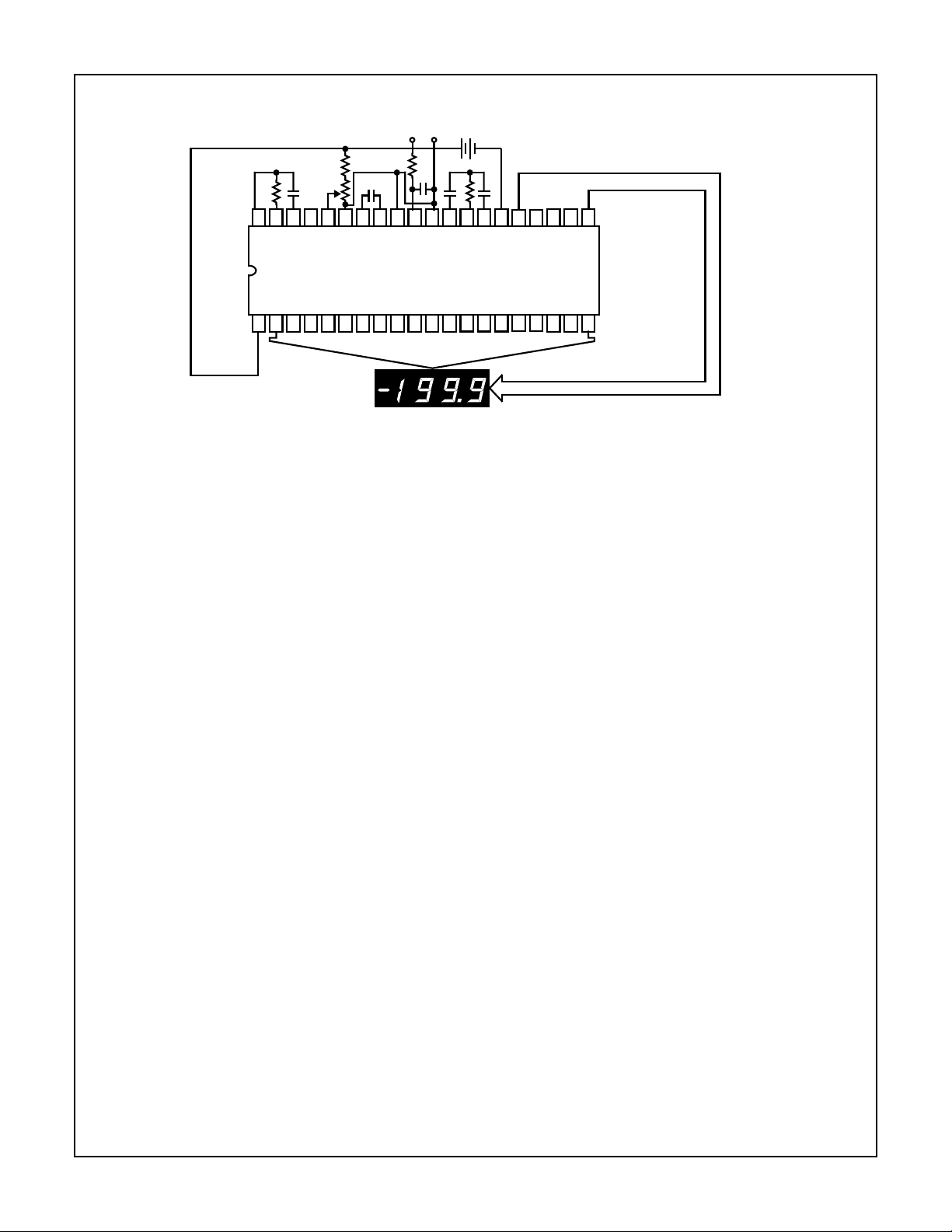
Typical Application and Test Circuit
HI7106
+-
R
C
+
REF
C
G1
1
5
-
REF
COM
C
E1
D2C2B2
HI7106
DISPLAY
R
1
R
C
4
OSC 3
TEST
4
REF HI
REF LO
F1
A1
R
3
4039383736353433323130
OSC 1
OSC 2
V+
D1C1B1
123456789
IN
C
5
C
R
2
IN HI
IN LO
101112
9V
+
-
C
2
3
28
29
27262524232221
V-
INT
A-Z
BUFF
F2
E2
A2
D3
13
14151617181920
DISPLAY
C3
G2
F3
B3
A3
E3
G3
AB4
BP
POL
FIGURE 1. HI7106 TEST CIRCUIT AND TYPICAL APPLICATION WITH LCD DISPLAY COMPONENTS
SELECTED FOR 200mV FULL SCALE
Design Information Summary Sheet
• OSCILLATOR FREQUENCY
f
= 0.45/RC
OSC
C
> 50pF; R
OSC
f
(Typ) = 48kHz
OSC
OSC
> 50kΩ
• OSCILLATOR PERIOD
t
= RC/0.45
OSC
• INTEGRATION CLOCK FREQUENCY
f
CLOCK
= f
OSC
/4
• INTEGRATION PERIOD
t
= 1000 x (4/f
INT
OSC
)
• 60/50Hz REJECTION CRITERION
t
INT/t60Hz
or t
lNT/t60Hz
= Integer
• OPTIMUM INTEGRATION CURRENT
I
= 4µA
INT
• FULL SCALE ANALOG INPUT VOLTAGE
V
(Typ) = 200mV or 2V
lNFS
• INTEGRATE RESISTOR
V
R
INT
---------------- -=
I
INFS
INT
• INTEGRATE CAPACITOR
t
()I
()
INT
C
INT
INT
--------------------------------=
V
INT
• INTEGRATOR OUTPUT VOLTAGE SWING
t
()I
()
INT
V
INT
INT
--------------------------------=
C
INT
•V
MAXIMUM SWING:
INT
(V- + 0.5V) < V
< (V+ - 0.5V), V
INT
• DISPLAY COUNT
V
IN
---------------
COUNT 1000
×=
V
REF
• CONVERSION CYCLE
t
CYC
t
CYC
when f
= t
= t
OSC
CL0CK
x 16,000
OSC
= 48kHz; t
x 4000
CYC
• COMMON MODE INPUT VOLTAGE
(V- + 1V) < V
< (V+ - 0.5V)
lN
• AUTO-ZERO CAPACITOR
0.01µF < C
AZ
< 1µF
• REFERENCE CAPACITOR
0.1µF < C
•V
COM
REF
< 1µF
Biased between Vi and V-.
COM
≅ V+ - 2.8V
•V
Regulation lost when V+ to V- < ≅6.8V
If V
the V
is externally pulled down to (V+ to V-)/2,
COM
circuit will turn off.
COM
• HI7106 POWER SUPPLY: SINGLE 9V
V+ - V- = 9V
Digital supply is generated internally
V
≅ V+ - 4.5V
GND
• HI7106 DISPLAY: LCD
Type: Direct drive with digital logic supply amplitude.
= 333ms
C1 = 0.1µF
C
C
C
C
R
R
R
R
R
(Typ) = 2V
INT
= 0.47µF
2
= 0.22µF
3
= 100pF
4
= 0.02µF
5
= 24kΩ
1
= 47kΩ
2
= 100kΩ
3
= 1kΩ
4
= 1MΩ
5
3

HI7106
Typical Integrator Amplifier Output Waveform (INT Pin)
AUTO ZERO PHASE
(COUNTS)
2999 - 1000
SIGNAL INTEGRATE
PHASE FIXED
1000 COUNTS
TOTAL CONVERSION TIME = 4000 x t
Detailed Description
Analog Section
Figure 2 shows the Analog Section for the HI7106. Each
measurement cycle is divided into three phases. They are
(1) auto-zero (A-Z), (2) signal integrate (INT) and (3) de-integrate (DE).
Auto-Zero Phase
During auto-zero three things happen. First, input high and
low are disconnected from the pins and internally shorted to
analog COMMON. Second, the reference capacitor is
charged to the reference voltage. Third, a feedback loop is
closed around the system to charge the auto-zero capacitor
C
to compensate for offset voltages in the buffer amplifier,
AZ
integrator,and comparator. Since the comparator is included
in the loop, the A-Z accuracy is limited only by the noise of
DE-INTEGRATE PHASE
0 - 1999 COUNTS
= 16,000 x t
CLOCK
OSC
the system. In any case, the offset referred to the input is
less than 10µV.
Signal Integrate Phase
During signal integrate, the auto-zero loop is opened, the
internal short is removed, and the internal input high and low
are connected to the external pins. The converter then
integrates the differential voltage between IN HI and IN LO
for a fixed time. This differential voltage can be within a wide
common mode range: up to 1V from either supply. If, on the
other hand, the input signal has no return with respect to the
converter power supply, IN LO can be tied to analog
COMMON to establish the correct common mode voltage. At
the end of this phase, the polarity of the integrated signal is
determined.
IN HI
COMMON
IN LO
STRAY STRAY
C
+
REF HI
REF
V+
31
32
30
34
10mA
INT
A-Z
INT
C
REF
36
A-Z A-Z
DE- DE+
DE+
A-Z AND DE( )
DE-
REF LO
35
FIGURE 2. ANALOG SECTION OF HI7106
R
INT
C
-
REF
33
-
+
INPUT
HIGH
N
V-
BUFFER
28 29 27
-
+
V+
1
2.8V
C
AZ
A-Z INT
INTEGRATOR
6.2V
INPUT
LOW
A-Z
-
+
COMPARATOR
C
INT
-
+
TO
DIGITAL
SECTION
4