HI5828
Data Sheet August 1999
12-Bit, 125+MSPS, CommLink™ Dual High
Speed CMOS D/A (2.7V-5.5V)
The HI5828is a Dual 12-bit, 125+MSPS (Mega Samples Per
Second), high speed, low power, D/A converter which is
implemented in an advanced CMOS process. Operating
from a single +3V to +5V supply, the converter provides
20mA of full scale output current and includes edge-triggered
CMOS input data latches. Low glitch energy and excellent
frequency domain performance is achieved by the HI5828’s
segmented current source architecture.
This device complements the CommLink HI5x60 and HI5x28
family of high speed converters, which includes 8, 10, 12,
and 14-bit devices
Ordering Information
TEMP.
PART
NUMBER
RANGE
(oC) PACKAGE PKG. NO.
CLOCK
SPEED
HI5828IN -40 to 85 48 Ld LQFP Q48.7x7A 125MSPS
HI5828EVAL2 25 Evaluation Platform 125MSPS
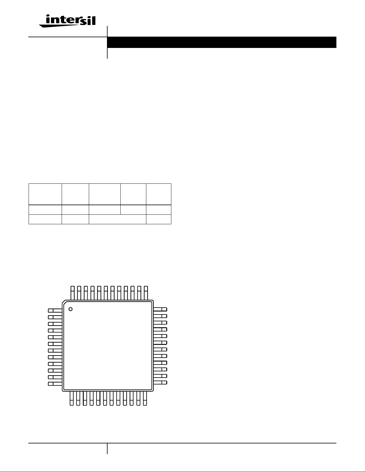
Pinout
HI5828
(LQFP)
TOP VIEW
File Number 4658.1
Features
• Throughput Rate . . . . . . . . . . . . . . . . . . . . . . .125+MSPS
• Low Power . . . . 312mW at 5V, 46mW at 3V (at 60MSPS)
• Integral Linearity Error
. . . . . . . . . . . . . . . . . . . ±0.75 LSB (Typ)
• Adjustable Full Scale Output Current. . . . . . 2mA to 20mA
• Internal 1.2V Bandgap Voltage Reference
• Single or Dual Power Supply from +3V to +5V
• Power Down Mode
• CMOS Compatible Inputs
• Excellent Spurious Free Dynamic Range
(76dBc, f
= 50MSPS, f
S
= 2.51MHz)
OUT
• Excellent Multitone Intermodulation Distortion
Applications
• Basestations (Cellular, WLL)
• Quadrature Modulation
• Wireless Communications Systems
• Direct Digital Frequency Synthesis
• Signal Reconstruction
• Medical/Test Instrumentation
ID5
ID4
ID3
ID2
ID1
(LSB) ID0
N.C.
N.C.
SLEEP
D
VDD
AGND
ICOMP2
ID6
1
2
3
4
5
6
7
8
9
10
11
12
13 14 15 16
VDD
A
ICOMP1
ID7
ID8
IOUTA
ID10
ID9
REFIO
IOUTB
N.C.
N.C.
ID11 (MSB)
AGND
FSADJ
REFLO
QD2
QD0 (LSB)
QD1
QOUTA
QOUTB
QCOMP1
• High Resolution Imaging Systems
• Arbitrary Waveform Generators
QD3
373839404142434445464748
36
35
34
33
32
31
30
29
28
27
26
25
2423222120191817
VDD
A
QD4
QD5
QD6
QD7
QD8
QD9
QD10
QD11 (MSB)
CLK
DGND
AGND
QCOMP2
1
CAUTION: These devices are sensitive to electrostatic discharge; follow proper IC Handling Procedures.
1-888-INTERSIL or 321-724-7143
CommLink™ is a trademark of Intersil Corporation.
| Copyright © Intersil Corporation 1999

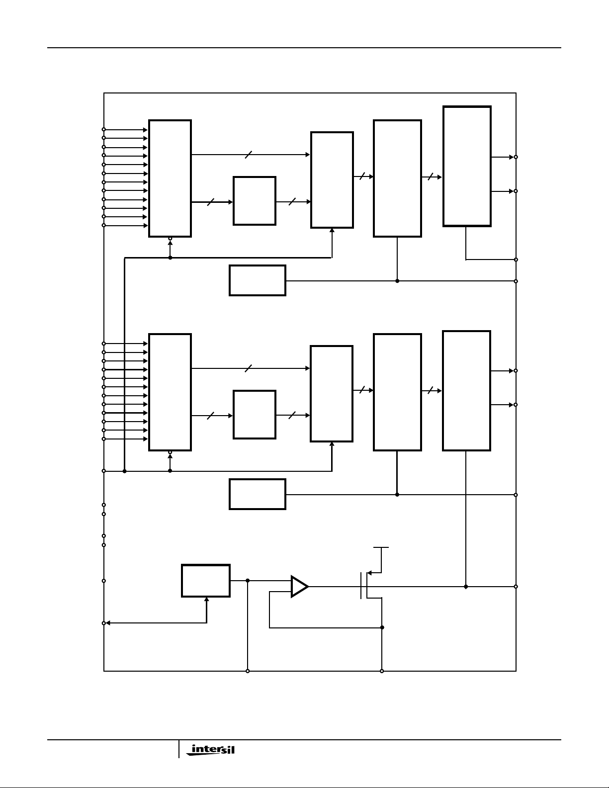
Functional Block Diagram
(LSB) QD0
QD1
QD2
QD3
QD4
QD5
QD6
QD7
QD8
QD9
QD10
(MSB) QD11
MASTER
LATCH
5
7
THERMO-
METER
DECODER
BIAS
GENERATION
HI5828
31
SLAVE
LATCH
38
SWITCH
DRIVERS
38
CURRENT
CELLS
7 LSBs
31 MSB
SEGMENTS
QOUTA
+
QOUTB
QCOMP1
QCOMP2
(LSB) ID0
ID1
ID2
ID3
ID4
ID5
ID6
ID7
ID8
ID9
ID10
(MSB) ID11
CLK
DVDD
DGND
AVDD
AGND
SLEEP
REFLO
MASTER
LATCH
5
BANDGAP
VOLTAGE
REFERENCE
7
THERMO-
METER
DECODER
BIAS
GENERATION
38
SLAVE
LATCH
31
-
+
SWITCH
DRIVERS
AVDD
38
CURRENT
CELLS
7 LSBs
31 MSB
SEGMENTS
+
IOUTA
IOUTB
ICOMP2
ICOMP1
REFIO FSADJ
2

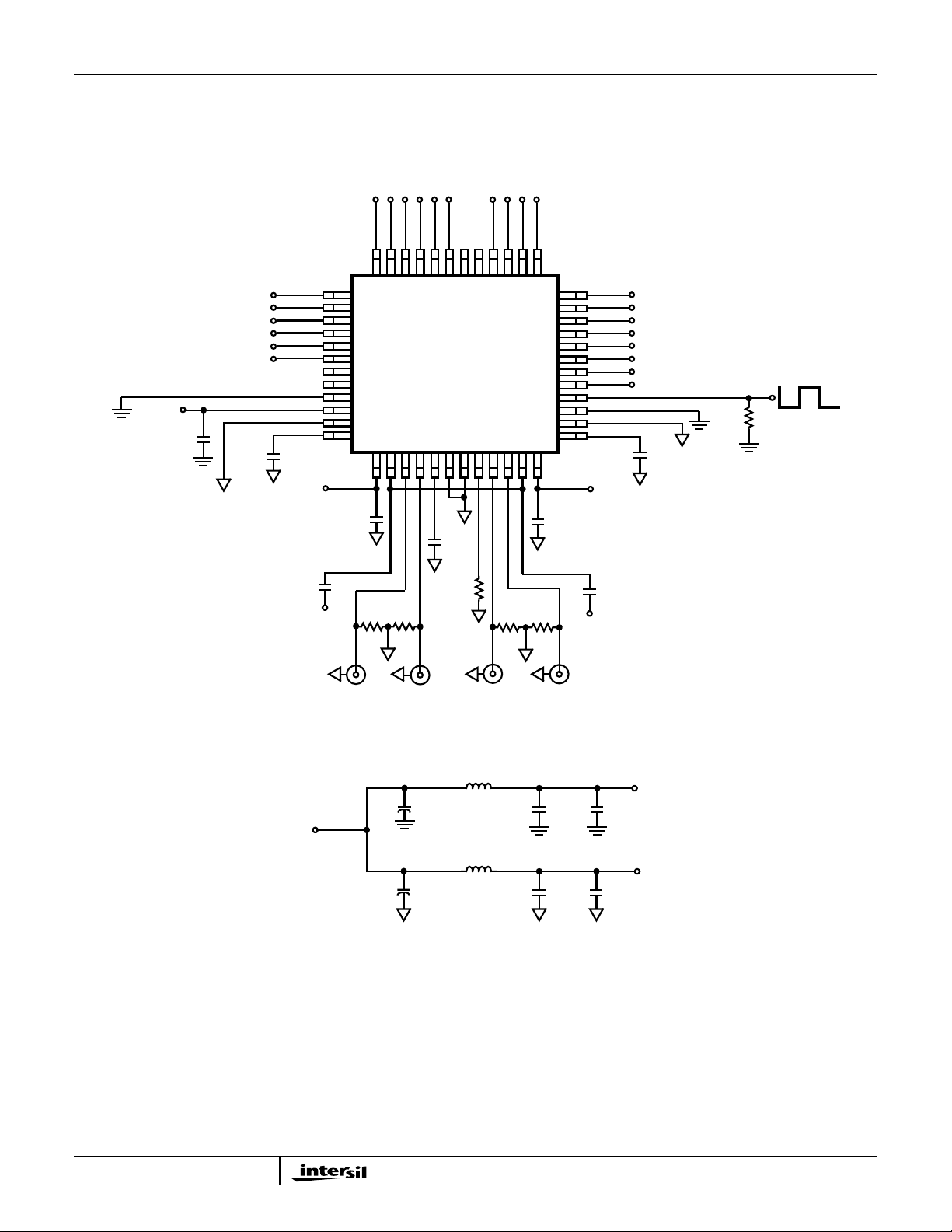
Typical Applications Circuit
ID5
ID4
ID3
ID2
ID1
ID0 (LSB)
SLEEP
DV
PP
C
0.1µF
1
C
0.1µF
ICOMP2
2
AV
PP
C
0.1µF
HI5828
QD0 (LSB)
QD1
QD2
CLK
DGND
AGND
R
4
50Ω
QD3
373839404142434445464748
36
35
34
33
32
31
30
29
28
27
26
25
2423222120191817
A
VDD
C
5
0.1µF
QCOMP1
R
5
50Ω
AV
PP
QCOMP2
AV
PP
C
8
0.1µF
QD4
QD5
QD6
QD7
QD8
QD9
QD10
QD11 (MSB)
C
3
0.1µF
R
50Ω
1
ID8
ID9
ID10
ID6
ID7
ID11 (MSB)
1
N.C.
2
3
N.C.
4
5
6
7
N.C.
N.C.
8
9
10
D
VDD
11
A
VDD
C
0.1µF
12
4
AGND
13 14 15 16
REFIO
REFLO
C
6
0.1µF
AGND
FSADJ
ICOMP1
7
R
2
50Ω
AV
PP
50Ω
R
SET
1.91kΩ
R
3
CONN
(IOUTA)
2
CONN
(QOUTB)
BEAD
FERRITE
L
1
10µH
CONN
1
(IOUTB)
C
+
11
10µF
3
CONN
(QOUTA)
C
9
0.1µF
4
DV
(DIGITAL POWER PLANE)
C
1µF
PP
10
+5V OR +3V POWER SOURCE
FERRITE
+
C
14
10µF
BEAD
L
2
10µH
C
12
0.1µF
C
1µF
AV
(ANALOG POWER PLANE)
PP
13
NOTE: Separate analog and digital grounds should be used, in which case the grounds should be tied together at a single point near the device.
The analog and digital grounds should be connected together by a thin single trace and never connected together by an inductor.
3

HI5828
Pin Descriptions
PIN NO. PIN NAME PIN DESCRIPTION
11, 19, 26 AGND Analog Ground.
13, 24 A
28 CLK Clock Input. The master and slave latches shown in the functional block diagram are simple D-latches.
27 DGND Connect to Digital Ground.
10 D
20 FSADJ Full Scale Current Adjust. Use a resistor to analog ground to adjust full scale output current. Full Scale
14, 23 ICOMP1, QCOMP1 Compensation Pin for Use in Reducing Bandwidth/Noise. Each pin should be individually decoupled to
12, 25 ICOMP2, QCOMP2 Compensation Pin for Internal Bias Generation. Each pin should be individually decoupled to AGND with
VDD
VDD
Analog Supply (+2.7V to +5.5V).
Input data to the DAC passes through the “master” latches when the clock is low and is latched into the
“master” latches when the clock is high. Data presented to the “slave” latch passes through when the
clock is logic high and is latched into the “slave”latches when the clock is logic low. Adequate setup time
must be allowed for the MSBs to pass through the thermometerdecoder before the clock goes high. This
master-slave arrangement comprises an edge-triggered flip-flop, with the DAC being updated on the
rising clock edge. It is recommended that the clock edge be skewed such that setup time is larger than
hold time for optimum spectral performance.
Digital Supply (+2.7V to +5.5V).
Output Current = 32 x V
on the REFIO pin (refer to the functional block diagram); which is typically 1.2V if the internal reference
is used.
AVDD with a 0.1µF capacitor. To minimize crosstalk, the part was designed so that these pins must be
connected externally, ideally directly under the device packaging. The voltage on these pins is used to
drive the gates of the PMOS devices that make up the current cells. Only the ICOMP1 pin is driven and
therefore QCOMP1 needs to be connected to ICOMP1, but de-coupled separately to minimize crosstalk.
If placed equally close to both pins, then only one decoupling capacitor might be necessary.
a 0.1µF capacitor. The voltage generated at these pins represents the voltage used to supply power to
the switch drivers (refer to the functional block diagram) which is 2.0V nominal. This arrangement helps
to minimize clock feedthrough to the current cell transistors for reduced glitch energy and improved
spectral performance.
FSADJ/RSET
. Where V
is the voltage at this pin. V
FSADJ
tracks the voltage
FSADJ
43-48, 1-6,
29-40
15, 22 IOUTA, QOUTA Current Outputs of the Device.Full scale output current is achievedwhen all input bits are set to binary 1.
16, 21 IOUTB, QOUTB Complementary Current Outputs of the Device. Full scale output current is achieved on the
7, 8, 41, 42 N.C. No Connection. Future LSBs for dual 14-bit DAC.
17 REFIO Reference voltage input if Internal reference is disabled. The internal reference is not intended to drive an
18 REFLO Reference Low Select. When the internal reference is enabled, this pin serves as the precision ground
9 SLEEP ControlPin for Power-Down Mode. Sleep Mode is active high; connect to ground for Normal Mode. The
ID11-ID0, QD11-QD0 Digital Data Input Ports. Bit 11 is Most Significant Bit (MSB) and bit 0 is the Least Significant Bit (LSB).
complementary outputs when all input bits are set to binary 0.
external load. Use 0.1µF cap to ground when internal reference is enabled.
reference point for the internal voltage reference circuitry and therefore needs to havea good connection
to analog ground to enable internal 1.2V reference. To disable the internal reference circuitry this pin
should be connected to A
Sleep pin has internal 25µA (nominal) active pulldown current.
VDD
.
4
 Loading...