

Intersil Corporation HI5702 Datasheet
HI5702
August 1997
Features
• Sampling Rate . . . . . . . . . . . . . . . . . . . . . . . . . 40 MSPS
• 8.3 Bits Guaranteed at f
= 10MHz
IN
• Low Power
• Wide Full Power Input Bandwidth . . . . . . . . . . 250MHz
• Sample and Hold Not Required
• Single-Ended or Differential Input
• Input Signal Range . . . . . . . . . . . . . . . . . . . . . . . . 1.25V
• Single Supply Voltage . . . . . . . . . . . . . . . . . . . . . . . .+5V
• TTL Compatible Interface
Applications
• Professional Video Digitizing
• Medical Imaging
• Digital Communication Systems
• High Speed Data Acquisition
10-Bit, 40 MSPS A/D Converter
Description
The HI5702 is a monolithic, 10-bit, analog-to-digital
converter fabricated in a BiCMOS process. It is designed for
high speed applications where wide bandwidth and low
power consumption are essential. Its 40 MSPS speed is
made possible by a fully differential pipeline architecture
which also eliminates the need for an external sample and
hold circuit. The HI5702 has excellent dynamic performance
while consuming <650mW power at 40 MSPS. Data output
latches are provided which present valid data to the output
bus with a latency of 7 clock cycles.
Refer to the HI5703, HI5746, or HI5767 data sheets for low er
power consumption.
Ordering Information
PART
NUMBER
HI5702KCB 40 MSPS 0 to 70 28 Ld SOIC (W) M28.3
HI5702JCB 36 MSPS 0 to 70 28 Ld SOIC (W) M28.3
SAMPLE
RATE
TEMP.
RANGE (oC) PACKAGE
PKG.
NO.
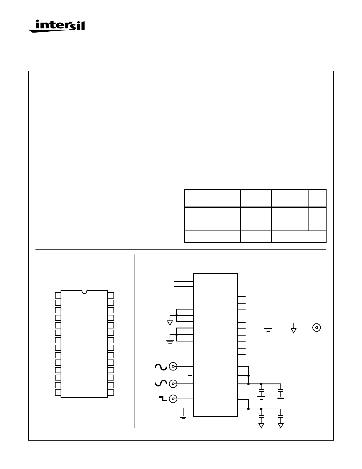
Pinout
DV
CC
DGND
DV
CC
DGND
AV
CC
AGND
V
+
REF
-
V
REF
+
V
IN
-
V
IN
V
CM
AGND
AV
CC
AGND
1
2
3
4
5
6
7
8
9
10
11
12
13
14
HI5702
(SOIC)
TOP VIEW
HI5702-EV2 25 Evaluation Board
Typical Application Schematic
HI5702
3.25V
2.0V
28
D0
27
D1
26
D2
25
D3
24
D4
23
DV
CC
22
CLK
21
DGND
20
D5
19
D6
18
D7
17
D8
16
D9
15
DFS
V
IN
VIN-
CLOCK
+
V
+ (7)
REF
V
- (8)
REF
(LSB) (28) D0
AGND (12)
AGND (6)
AGND (14)
DGND (2)
DGND (21)
DGND (4)
(MSB) (16) D9
V
+ (9)
IN
VCM(11)
V
- (10)
IN
CLK (22)
DFS (15)
(27) D1
(26) D2
(25) D3
(24) D4
(20) D5
(19) D6
(18) D7
(17) D8
(1) DV
(3) DV
(23) DV
(13) AV
(5) AV
CC
CC
CC
CC
CC
D0
D1
D2
D3
D4
D5
D6
D7
D8
D9
DGND
0.1µF
0.1µF 10µF
AGND
10µF AND 0.1µF CAPS
ARE PLACED AS CLOSE
TO PART AS POSSIBLE
+
10µF
+
BNC
CAUTION: These devices are sensitive to electrostatic discharge; follow proper IC Handling Procedures.
1-888-INTERSIL or 321-724-7143 | Copyright © Intersil Corporation 1999
4-1505
File Number 3745.4
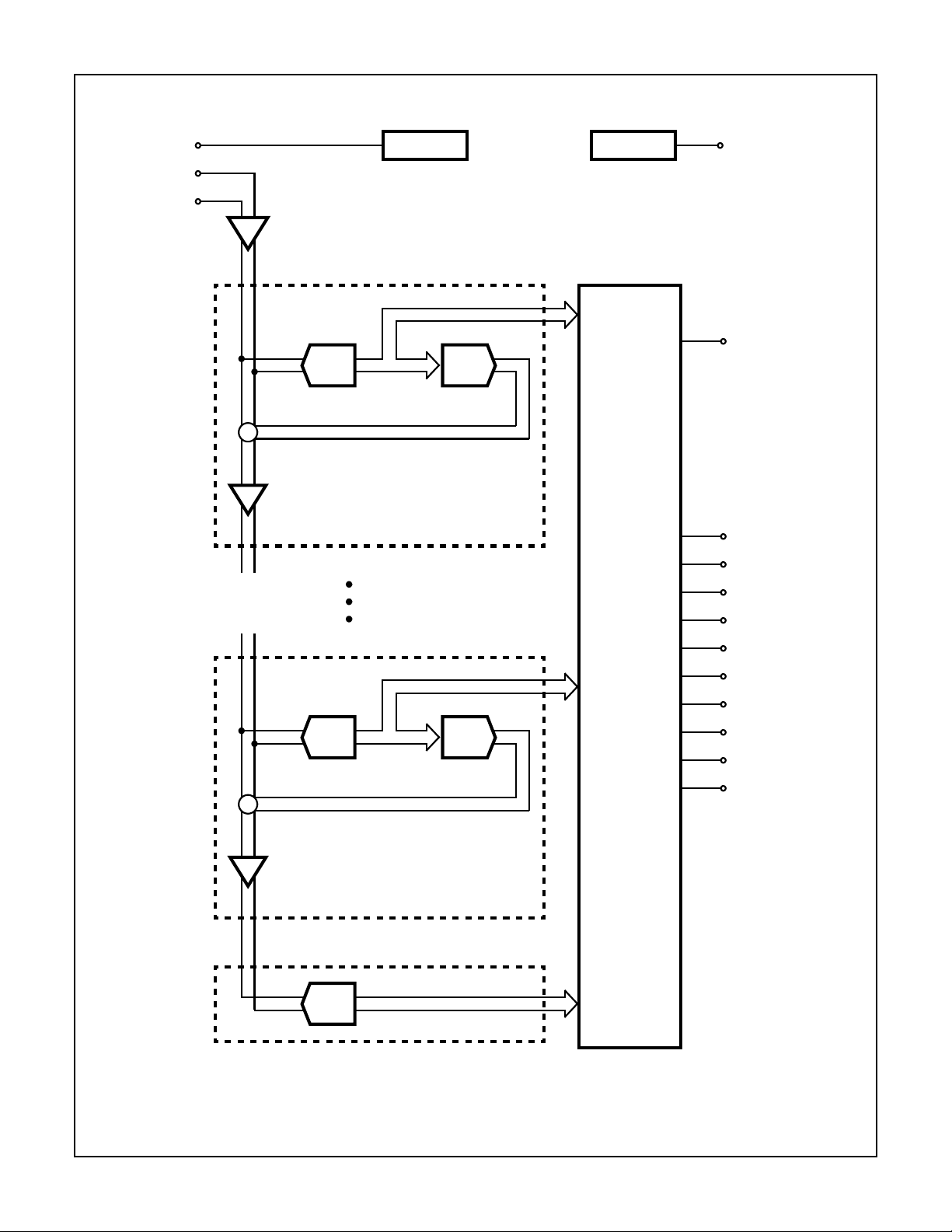
Functional Block Diagram
HI5702
V
VIN-
V
CM
IN
BIAS
+
S/H
STAGE 1
X2
2-BIT
FLASH
+
-
∑
2-BIT
DAC
CLOCK
CLK
DFS
D9 (MSB)
D8
D7
X2
D6
STAGE 9
2-BIT
FLASH
+
-
∑
STAGE 10
1-BIT
FLASH
2-BIT
DAC
DIGITAL DELAY
AND
DIGITAL ERROR
CORRECTION
D5
D4
D3
D2
D1
D0 (LSB)
AV
CC
AGND DV
CC
DGND V
4-1506
+V
REF
REF
-
HI5702
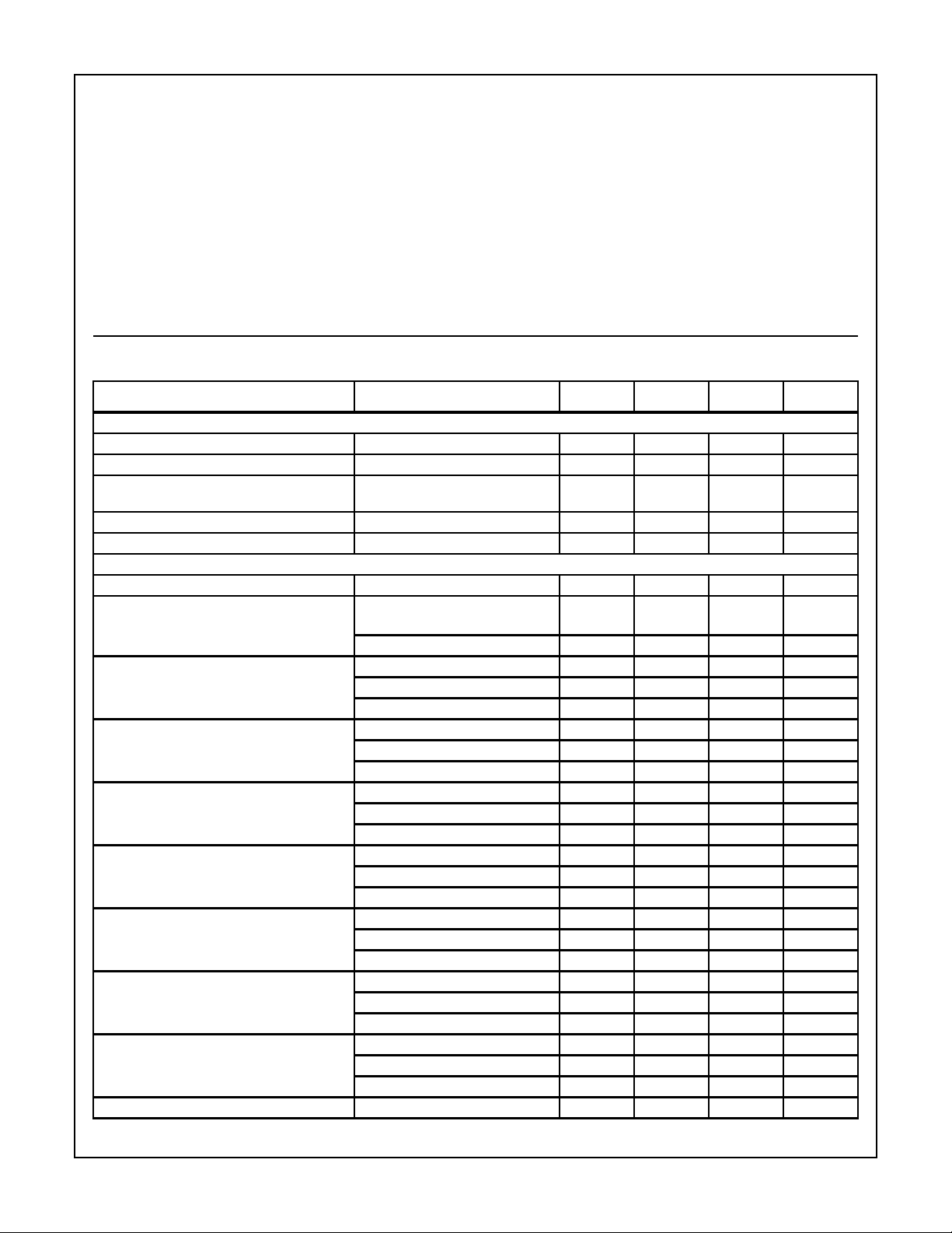
Absolute Maximum Ratings Thermal Information
Supply Voltage, AVCC or DVCC to AGND or DGND. . . . . . . . . . +6V
DGND to AGND . . . . . . . . . . . . . . . . . . . . . . . . . . . . . . . . . . . . . . . .0.3V
Digital I/O Pins . . . . . . . . . . . . . . . . . . . . . . . . . . . . . DGND to DV
Analog I/O Pins. . . . . . . . . . . . . . . . . . . . . . . . . . . . . AGND to AV
Operating Conditions
Temperature Range
HI5702KCB/JCB. . . . . . . . . . . . . . . . . . . . . . . . . . . . .0oC to 70oC
CAUTION: Stresses above those listed in “Absolute Maxim um Ratings” ma y cause permanent damage to the device . This is a stress only rating and oper ation of
the device at these or any other conditions above those indicated in the operational sections of this specification is not implied.
NOTE:
9. θJA is measured with the component mounted on an evaluation PC board in free air.
Thermal Resistance (Typical, Note 1) θJA (oC/W)
SOIC Package. . . . . . . . . . . . . . . . . . . . . . . . . . . . . 70
CC
Maximum Junction Temperature. . . . . . . . . . . . . . . . . . . . . . . 150oC
CC
Maximum Storage Temperature Range . . . . . . . . . -65oC to 150oC
Maximum Lead Temperature (Soldering, 10s) . . . . . . . . . . . . 300oC
(SOIC - Lead Tips Only)
Electrical Specifications AV
PARAMETER TEST CONDITIONS MIN TYP MAX UNITS
ACCURACY
Resolution 10 - - Bits
Integral Linearity Error, INL f
Differential Linearity Error, DNL
(Guaranteed No Missing Codes)
Offset Error, V
Full Scale Error, FSE fIN = DC - 2 - LSB
DYNAMIC CHARACTERISTICS
Minimum Conversion Rate No Missing Codes - 0.5 - MSPS
Maximum Conversion Rate No Missing Codes
Effective Number of Bits, ENOB f
Signal to Noise and Distribution Ratio,
SINAD
--------------------------------------------------------------=
RMS Noise + Distortion
Signal to Noise Ratio, SNR fIN = 1MHz - 56 - dB
RMS Signal
-------------------------------- -=
RMS Noise
Total Harmonic Distortion, THD fIN = 1MHz - -64 - dBc
2nd Harmonic Distortion fIN = 1MHz - -75 - dBc
3rd Harmonic Distortion fIN = 1MHz - -66 - dBc
Spurious Free Dynamic Range, SFDR fIN = 1MHz - 66 - dBc
Intermodulation Distortion, IMD f1 = 1MHz, f2 = 1.02MHz - -59 - dBc
OS
RMS Signal
= DVCC = +5V; V
CC
= 20pF; TA = 25oC; Unless Otherwise Specified
C
L
= DC - ±1 ±2.0 LSB
IN
fIN = DC - ±0.5 ±1 LSB
fIN = DC - 3 - LSB
HI5702KCB 40 - - MSPS
HI5702JCB 36 - - MSPS
= 1MHz - 9.0 - Bits
IN
fIN = 5MHz - 9.0 - Bits
fIN = 10MHz 8.3 8.8 - Bits
fIN = 1MHz - 57 - dB
fIN = 5MHz - 57 - dB
fIN = 10MHz 51 56 - dB
fIN = 5MHz - 56 - dB
fIN = 10MHz 51 55 - dB
fIN = 5MHz - -63 - dBc
fIN = 10MHz - -60 - dBc
fIN = 5MHz - -75 - dBc
fIN = 10MHz - -73 - dBc
fIN = 5MHz - -64 - dBc
fIN = 10MHz - -63 - dBc
fIN = 5MHz - 64 - dBc
fIN = 10MHz 54 63 - dBc
+ = 3.25V; V
REF
REF
- = 2V; fS = Specified Clock Frequency at 50% Duty Cycle;
4-1507
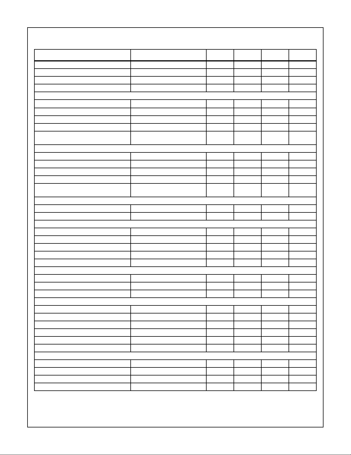
HI5702
Electrical Specifications AV
= DVCC = +5V; V
CC
+ = 3.25V; V
REF
- = 2V; fS = Specified Clock Frequency at 50% Duty Cycle;
REF
CL = 20pF; TA = 25oC; Unless Otherwise Specified (Continued)
PARAMETER TEST CONDITIONS MIN TYP MAX UNITS
Differential Gain Error fS = 17.72MHz, 6 Step, Mod Ramp - 0.5 1 %
Differential Phase Error fS = 17.72MHz, 6 Step, Mod Ramp - 0.25 0.5 Degree
Transient Response - 1 - Cycle
Overvoltage Recovery 0.2V Overdrive - 1 - Cycle
ANALOG INPUT
Analog Input Resistance, R
Analog Input Capacitance, C
Analog Input Bias Current, I
IN
IN
B
(Note 3) - 1
-
MΩ
-7-pF
(Note 3) -50 - +50 µA
Full Power Input Bandwidth - 250 - MHz
Analog Input Common Mode Range
Differential Mode (Note 2) 0.625 - 4.375 V
(VIN++ VIN-) / 2
REFERENCE INPUT
Total Reference Resistance, R
L
200 400 - Ω
Reference Current - 3 6 mA
Positive Reference Input, V
Negative Reference Input, V
Reference Common Mode Voltage
(V
REF
++ V
REF
-) / 2
+ (Note 2) - 3.25 3.3 V
REF
- (Note 2) 1.95 2.0 - V
REF
(Note 2) 2.575 2.625 2.675 V
COMMOM MODE VOLTAGE
Common Mode Voltage Output, V
CM
- 2.8 - V
Max Output Current - - 1 mA
DIGITAL INPUTS
Input Logic High Voltage, V
Input Logic Low Voltage, V
Input Logic High Current, I
Input Logic Low Current, I
Input Capacitance, C
IN
IH
IL
IH
IL
VIN = 5V - - 10.0 µA
VIN = 0V - - 10.0 µA
2.0 - - V
- - 0.8 V
-7-pF
DIGITAL OUTPUTS
Output Logic Sink Current, I
OL
Output Logic Source Current, I
Output Capacitance, C
OUT
OH
VO = 0.4V 3.2 - - mA
VO = 2.4V -0.2 - - mA
-5-pF
TIMING CHARACTERISTICS
Aperture Delay, t
Aperture Jitter, t
AP
AJ
Data Output Delay, t
Data Output Hold, t
Data Latency, t
LAT
OD
H
For a Valid Sample (Note 2) - - 7 Cycles
-5-ns
-5-ps
-6-ns
-5-ns
Power-Up Initialization Data Invalid Time (Note 2) - - 20 Cycles
POWER SUPPLY CHARACTERISTICS
Supply Current, I
CC
VIN = 0V - 120 130 mA
Power Dissipation VIN = 0V - 600 650 mW
Offset Error PSRR, ∆V
OS
AVCCor DVCC = 5V ±5% - 0.2 - LSB
Gain Error PSRR, ∆FSE AVCC or DVCC = 5V ±5% - 1 - LSB
NOTES:
10. Parameter guaranteed by design or characterization and not production tested.
11. With the clock off.
4-1508
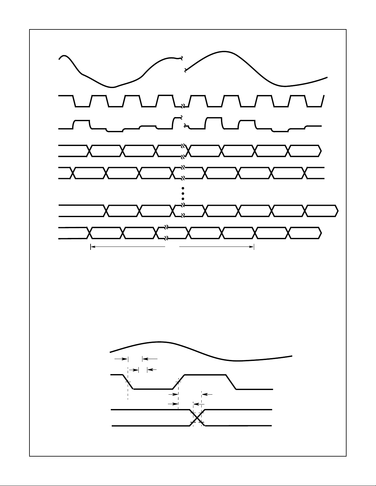
Timing Waveforms
ANALOG
INPUT
HI5702
CLOCK
INPUT
S
N - 1HN - 1SN
HNS
N + 1HN + 1SN + 2
INPUT
S/H
1ST
STAGE
2ND
STAGE
10TH
STAGE
DAT A
UTPUT
B
2, N - 2
B
1, N - 1
D
N - 7
B
2, N - 1
B
10, N - 5
B
D
1, N
N - 6
B
2, N
B
10, N - 4
B
NOTES:
1. SN: N-th sampling period.
2. HN: N-th holding period.
3. B
: M-th stage digital output corresponding to N-th sampled input.
M, N
4. DN: Final data output corresponding to N-th sampled input.
FIGURE 8. HI5702 INTERNAL CIRCUIT TIMING
1, N + 1
t
LAT
S
N + 5HN + 5SN + 6HN + 6SN + 7HN + 7SN + 8HN + 8
B
1, N + 4
D
N - 2
B
2, N + 4
B
10, N
B
1, N + 5
D
N - 1
B
2, N + 5
B
10, N + 1
B
1, N + 6
D
N
B
2, N + 6
B
10, N + 2
B
1, N + 7
D
N + 1
B
10, N + 3
ANALOG
INPUT
CLOCK
INPUT
DAT A
OUTPUT
1.5V
t
AP
t
AJ
1.5V
t
OD
t
H
2.0V
DATA N - 1
0.8V
FIGURE 9. INPUT-TO-OUTPUT TIMING
4-1509
DATA N
 Loading...