


HI5675
Data Sheet April 1999 File Number 4711
8-Bit, 20MSPS, Flash A/D Converter
The HI5675 is an 8-bit, analog-to-digital converter built in an
advanced CMOS process. The low power, low differential
gain and phase, high sampling rate, and single 5V supply
make the HI5675 ideal for video and imaging applications.
The adoption of a 2-step flash architecture achieves low
power consumption (60mW) at a maximum conversion
speed of 20MSPS with only a 2.5 clock cycle data latency.
The HI5675 also features digital output enable/disable and a
built in voltage reference. The HI5675 can be configured to
use the internal reference or an external reference if higher
precision is required.
Ordering Information
TEMP.
PART NUMBER
RANGE (oC) PACKAGE PKG. NO.
HI5675JCB -40 to 85 24 Ld SOIC M24.2-S
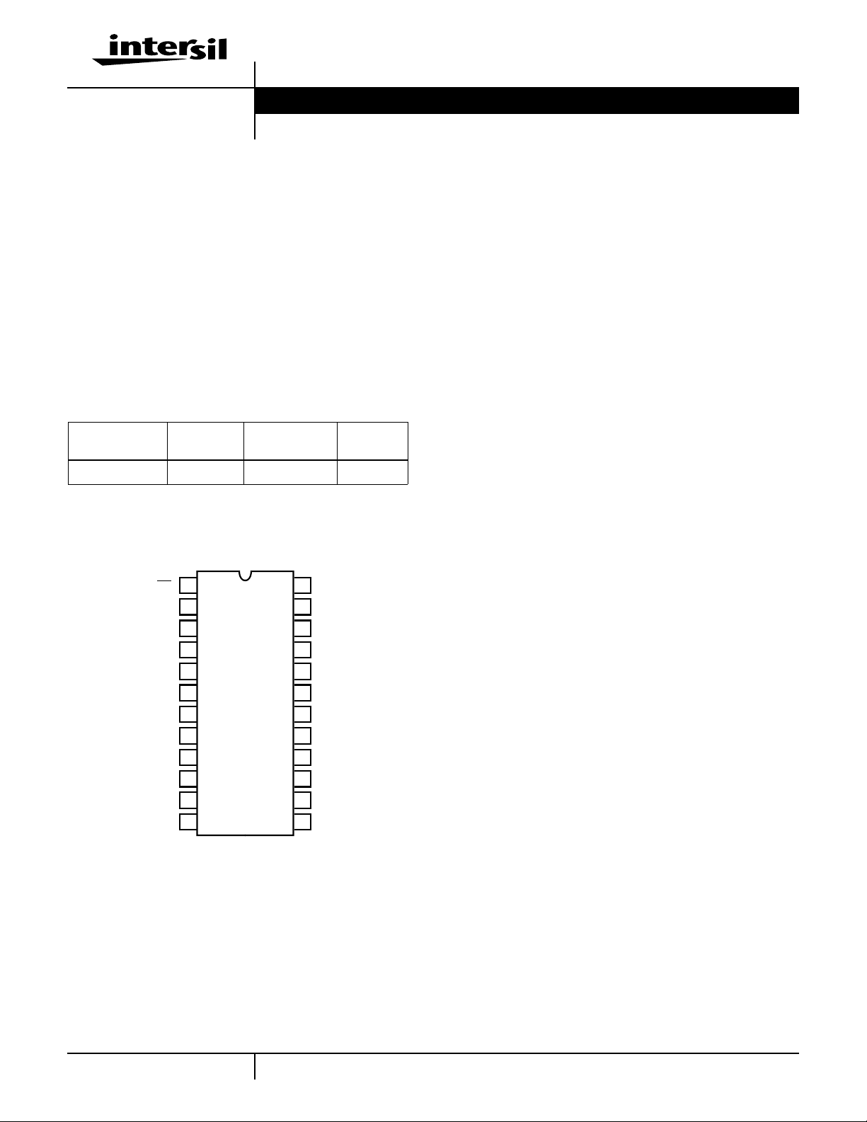
Pinout
HI5675 (SOIC)
TOP VIEW
Features
• Resolution . . . . . . . . . . . . . . . . . . . .8-Bit ±0.3 LSB (DNL)
• Maximum Sampling Frequency . . . . . . . . . . . . . .20MSPS
• Low Power Consumption . . . . . . . . . . . . . . . . . . . . .60mW
(Reference Current Excluded)
• Built-In Sample and Hold Circuit
• Built-In Reference Voltage Self Bias Circuit
• Three-State TTL Compatible Output
• Single +5V Power Supply
• Low Input Capacitance. . . . . . . . . . . . . . . . . . . 11pF (Typ)
• Reference Impedance . . . . . . . . . . . . . . . . . . . 300Ω (Typ)
• Low Cost
• Direct Replacement for TLC5510 and ADC1175
Applications
• Video Digitizing
• PC Video Capture
• Image Scanners
OE
DV
SS
D0 (LSB)
D1
D2
D3
D4
D5
D6
D7 (MSB)
DV
DD
CLK
1
2
3
4
5
6
7
8
9
10
11
12
24
DV
SS
23
V
RB
22
V
RBS
21
AV
SS
20
AV
SS
19
V
IN
18
AV
DD
17
V
RT
16
V
RTS
15
AV
DD
14
AV
DD
13
DV
DD
• TV Set Top Boxes
• Multimedia
• Personal Communication Systems (PCS)
1
CAUTION: These devices are sensitive to electrostatic discharge; follow proper IC Handling Procedures.
1-888-INTERSIL or 321-724-7143
| Copyright © Intersil Corporation 1999

Functional Block Diagram
HI5675
1
OE
DV
2
SS
DV
D1
D2
D3
D4
D5
D6
DD
CLK
3
4
5
6
7
8
9
10
11
12
LOWER
DAT A
LATCHES
UPPER
DAT A
LATCHES
CLOCK GENERATOR
D0 (LSB)
D7 (MSB)
Typical Application Schematic
LOWER
ENCODER
(4-BIT)
LOWER
ENCODER
(4-BIT)
UPPER
ENCODER
(4-BIT)
LOWER
COMPARATORS
WITH S/H (4-BIT)
LOWER
COMPARATORS
WITH S/H (4-BIT)
UPPER
COMPARATORS
WITH S/H (4-BIT)
REFERENCE VOLTAGE
24
DV
23
V
V
22
0.6V (Typ)
21
AV
20
AV
19
V
18
AV
V
17
V
16
2.6V (Typ)
15
AV
14
AV
DV
13
SS
RB
RBS
SS
SS
IN
DD
RT
RTS
DD
DD
DD
HC04
+5V
R11
ICL8069
: Ceramic Chip Capacitor 0.1µF
†
R12
V
IN
CA158A
+
-
R3
+
-
R1
R4
R13
R5
CA158A
HA2544
+
-
R2
C11
0.1µF
C12
0.1µF
C9
4.7µF
C10
0.1µF
C7
4.7µF
C8
+
CLOCK IN
+5V
+
13
14
15
16
17
18
†
+5V
19
20
21
22
23
24
HI5675
12
11
10
9
8
7
6
5
4
3
2
1
CLK
D7 (MSB)
D6
D5
D4
D3
D2
D1
D0 (LSB)
: Analog GND
: Digital GND
NOTE: It is necessary that AVDDand DVDDpins be driven from the same supply. The gain of analog input signal can be changed by adjusting the
ratio of R2 to R1.
2

HI5675
Pin Descriptions
PIN
NUMBER SYMBOL DESCRIPTION
1 OE When OE = Low, Data is valid. When OE = High, D0 to D7 pins high impedance.
2, 24 DV
3-10 D0 to D7 D0 (LSB) to D7 (MSB) Output.
11, 13 DV
12 CLK Clock Input.
16 V
17 V
23 V
14, 15, 18 AV
19 V
20, 21 AV
22 V
SS
DD
RTS
RT
RB
DD
IN
SS
RBS
Digital GND.
Digital +5V. (Connect to AVDDto avoid Latchup).
Shorted with VRT generates, +2.6V.
Reference Voltage (Top).
Reference Voltage (Bottom).
Analog +5V. Digital +5V. (Connect to DVDDto avoid Latchup).
Analog Input.
Analog GND.
Shorted with VRB generates +0.6V.
3