


HI5634
PRELIMINARY
Data Sheet May 1999
High Performance Programmable
Phase-Locked Loop for LCD Applications
The HI5634 is a low cost but very high-performance
frequency generator for line-locked and genlocked high
resolution video applications. Utilizing an advanced low
voltage CMOS mixed signal technology, the HI5634 is an
effective clock solution for video projectors and displays at
resolutions from VGA to beyond UXGA
The HI5634 offers pixel clock outputs in both differential (to
250MHz) and single-ended (to 150MHz) formats. Digital
phase adjustment circuitry allows user control of the pixel
clock phase relative to the recovered sync signal. A second
differential output at half the pixel clock rate enables
deMUXing of multiplexed A/D converters. The FUNC pin
provides either the regenerated input from the phase-locked
loop (PLL) divider chain output or a re-synchronized and
sharpened input HSYNC.
The advanced PLL utilizes either its internal programmable
feedback divider or an external divider. The device is
programmed by a standard I
2
C-bus® serial interface.
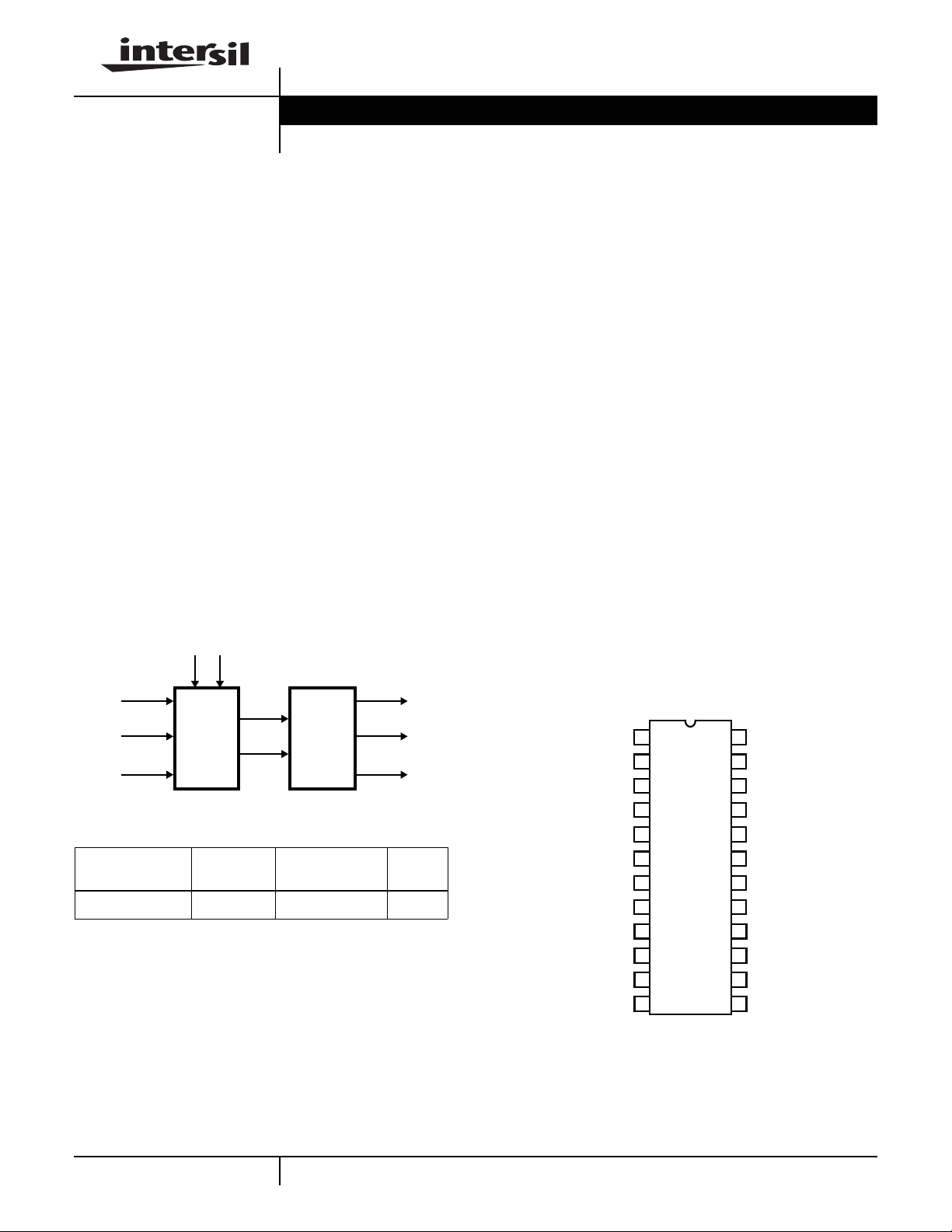
Simplified Block Diagram
File Number
Features
• Pixel Clock Frequencies up to 250MHz
• Very Low Jitter
• Digital Phase Adjustment (DPA) for Clock Outputs
• Balanced PECL Differential Outputs
• Single-Ended SSTL_3 Clock Outputs
• Double-Buffered PLL/DPA Control Registers
• Independent Software Reset for PLL/DPA
• External or Internal Loop Filter Selection
• Uses 3.3V Supply. Inputs are 5V Tolerant.
2
C-bus Serial Interface can Run at Either Low Speed
•I
(100kHz) or High Speed (400kHz)
• Lock Detection
Applications
• LCD Monitors and Video Projectors
• Genlocking Multiple Video Subsystems
• Frequency Synthesis
4745
LOOP FILTER
OSC
HSYNC
2
I
C INTERFACE
PHASE
LOCKED
LOOP
DIGITAL
PHASE
ADJUST
Ordering Information
TEMP.
PART NUMBER
HI5634CB 0 to 70 24 Ld SOIC M24.3
RANGE (oC) PACKAGE
PKG.
CLK
CLK/2
FUNC
NO.
Pinout
VDDD
VSSD
SDA
SCL
PDEN
EXTFB
HSYNC
EXTFIL
EXTFILRET
VDDA
VSSA
OSC
1
2
3
4
5
6
7
8
9
10
11
12
HI5634
(SOIC)
TOP VIEW
24
IREF
23
CLK/2+ (PECL)
22
CLK/2- (PECL)
21
CLK+ (PECL)
20
CLK- (PECL)
19
VSSQ
18
VDDQ
17
CLK (SSTL)
16
CLK/2 (SSTL)
15
FUNC (SSTL)
14
LOCK/REF (SSTL)
2
CADR
13
I
1
CAUTION: These devices are sensitive to electrostatic discharge; follow proper IC Handling Procedures.
http://www.intersil.com or 407-727-9207
I2C Bus is a Trademark of Philips Corporation.
| Copyright © Intersil Corporation 1999

HI5634
Pin Descriptions
PIN NO. PIN NAME TYPE DESCRIPTION COMMENTS
1 VDDD PWR Digital Supply 3.3V to Digital Sections
2 VSSD PWR Digital Ground
3 SDA IN/OUT Serial Data I2C-Bus (Note 1)
4 SCL IN Serial Clock I2C-Bus (Note 1)
5 PDEN IN PFD Enable Suspends Charge Pump (Note1)
6 EXTFB IN External Feedback In External Divider Input to PFD (Note1)
7 HSYNC IN Horizontal Sync Clock Input to PLL (Note1)
8 EXTFIL IN External Filter External PLL Loop Filter
9 EXTFILRET IN External Filter Return External PLL Loop Filter Return
10 VDDA PWR Analog Supply 3.3V for Analog Circuitry
11 VSSA PWR Analog Ground Ground for Analog Circuitry
12 OSC IN Oscillator Input From Crystal Oscillator Package (Notes 1, 2)
13 I2CADR IN I2C Address Chip I2C Address Select
Low = 4Dh Read, 4Ch Write
High = 4Fh Read, 4Eh Write
14 LOCK/REF (SSTL) OUT Lock Indicator/Reference Displays PLL or DPA Lock or REF Input
15 FUNC (SSTL) OUT Function Output SSTL_3 Selectable HSYNC Output
16 CLK/2 (SSTL) OUT Pixel Clock/2 Out SSTL_3 Driver to ADC DeMUX Input
17 CLK (SSTL) OUT Pixel Clock Out SSTL_3 Driver to ADC
18 VDDQ PWR Output Driver Supply 3.3V to Output Drivers
19 VSSQ PWR Output Driver Ground Ground for Output Drivers
20 CLK- (PECL) OUT Pixel Clock Out Inverted PECL Driver to ADC. Open Drain Output.
21 CLK+ (PECL) OUT Pixel Clock Out PECL Driver to ADC. Open Drain Output.
22 CLK/2- (PECL) OUT Pixel Clock/2 Out Inverted PECLDriverto ADC DeMUXInput.Open Drain
Output.
23 CLK/2+ (PECL) OUT Pixel Clock/2 Out PECL Driver to ADC DeMUX Input. Open DrainOutput.
24 IREF IN Reference Current Reference Current for PECL Outputs
NOTES:
1. These LVTTL inputs are 5V tolerant.
2. Connect to ground if unused.
2

Block Diagram
HI5634
EN_DLS
REG 0[7]
EXTFIL (8) XFILRET (9)
EN_PLS
REG 0[6]
IREF (24)
BIAS
PECL
VCO
FILTER
SELECT
PUMP
CHARGE
PSD
FIL_SEL
REG 4[7]
OUT_SCL
REG 6[6-7]
REG 1[4-5]
POST
DIVIDER
SCALER
INT FILTER
OE_TCK
CLK (17)
OUTPUT
SCALER
REG 6[1]
CLK+ (21)
+
OE_PCK
REG 6[0]
CLK- (20)
OE_T2
REG 6[3]
CLK/2 (16)
PHASE
DIGITAL
OE_P2
REG 6[2]
CLK/2+ (23)
CLK/2- (22)
+
ADJUST
OE_F
REG 6[4]
FUNC (15)
PDEN (5)
OSC_DIV
REG 7[0-6]
LOCK
LOCK/REF (14)
PDEN
REG 0[0]
PD_POL
REG 0[1]
OSC
DIVIDER
OSC (12)
LOGIC
REG 0[2]
REF_POL
1
FREQ
PHASE/
MUX
0
HSYNC (7)
DETECTOR
IN_SEL
PLL_LOCK
PFD
REG 7[7]
FBK_SEL
REG 12[1]
DPA_LOCK
REG 1[0-2]
REG 0[3]
FBK_POL
REG 0[4]
REG 12[0]
MUX
1
0
EXTFB (6)
FEEDBACK
DIVIDER
FBD1
REG 3[0-3]
FBD0
REG 2[0-7]
DPA_OS
C
2
I
SDA (3)
DPA_RES
REG 4[0-5]
REG 5[0-1]
INTERFACE
SCL (4)
CADR (13)
2
I
CK2_INV
REG 6[5]
POWER
1
ON
MUX
0
RESET
REG 0[5]
FUNC_SEL
3
HI5634
Absolute Maximum Ratings Thermal Information
VDDA, VDDD, VDDQ (Measured to VSS) . . . . . . . . . . . . . . . . . 4.3V
Digital Inputs . . . . . . . . . . . . . . . . . . . . . . . . . .VSSD -0.3V to +5.5V
Analog Outputs . . . . . . . . . . . . . . . . . . VSSA -0.3V to VDDA +0.3V
Digital Pouts. . . . . . . . . . . . . . . . . . . . . VSSQ -0.3V to VDDQ +0.3V
ESD Rating
Human Body Model (Per MIL-STD-883 Method 3015.7). . . >2kV
Operating Conditions
Temperature Range . . . . . . . . . . . . . . . . . . . . . . . . . . . 0oC to 70oC
Voltage Range (VDDA, VDDD, VDDQ to VSS) . . . . . . 3.0V to 3.6V
CAUTION: Stresses above those listed in “Absolute Maximum Ratings” may cause permanent damage to the device. This is a stress only rating and operationofthe
device at these or any other conditions above those indicated in the operational sections of this specification is not implied.
NOTE:
3. θJA is measured with the component mounted on an evaluation PC board in free air.
Electrical Specifications Per Operating Conditions Listed Above, Unless Otherwise Specified
PARAMETER SYMBOL TEST CONDITIONS MIN TYP MAX UNITS
DC SUPPLY CURRENT
Supply Current, Digital IDDD VDDD = 3.6V - - 25 mA
Supply Current, Output Drivers IDDQ VDDQ = 3.6V, No Output Drivers Enabled - - 6 mA
Supply Current, Analog IDDA VDDA = 3.6V - - 5 mA
DIGITAL INPUTS (SDA, SCL, PDEN, EXTFB, HSYNC, OSC, I
Input High Voltage V
Input Low Voltage V
IH
IL
Input Hysteresis 0.2 - 0.6 V
Input High Current I
Input Low Current I
Input Capacitance C
VIH = VDD - - ±10 µA
IH
VIL = 0 - - ±200 µA
IL
IN
SDA (IN OUTPUT MODE: SDA IS BIDIRECTIONAL)
Output Low Voltage V
OL
I
OUT
Determined by the External Pull-up Resistor.
PECL OUTPUTS (CLK+, CLK-, CLK/2+, CLK/2-)
Output High Voltage V
Output Low Voltage (Note 4) V
OHIOUT
I
OL
OUT
SSTL_3 OUTPUTS (CLK, CLK/2, FUNC, LOCK/REF)
Output Resistance R
1 < VO< 2V - - 80 Ω
O
AC INPUT CHARACTERISTICS
HSYNC Input Frequency f
OSC Input Frequency f
HSYNC
OSC
Reg 7[7] = 0 0.008 - 10 MHz
Reg 7[7] = 1 0.02 - 100 MHz
TIMING CHARACTERISTICS (Note 5)
REF Output Transition Times t
PECL CLK Output Transition Times t
SSTL CLK Output Transition Times t
FUNC Output Transition Times t
HSYNC to REF Delay t
REF to PECL Clock Delay t
Rise Time/Fall Time - 2.8/1.8 - ns
r
Rise Time/Fall Time - 1.0/1.2 - ns
P
Rise Time/Fall Time - 1.6/0.7 - ns
S
Rise Time/Fall Time - 1.2/1.0 - ns
F
0
1
2
CADR)
= 3mA. VOH = 6.0V Maximum, as
= 0 - - VDD V
= Programmed Value 1.0 - - V
Thermal Resistance (Typical, Note 3) θJA (oC/W)
SOIC Package . . . . . . . . . . . . . . . . . . . . . . . . . . . . . 80
Maximum Junction Temperature (Plastic Package) . . . . . . . .150oC
Maximum Storage Temperature Range. . . . . . . . . . -65oC to 150oC
Maximum Lead Temperature (Soldering 10s) . . . . . . . . . . . . 260oC
(SOIC - Lead Tips Only)
2 - 5.5 V
VSS-0.3 - 0.8 V
- - 10 pF
- - 0.4 V
11.3 11.5 12 ns
-1.0 0.8 2.2 ns
4
HI5634
Electrical Specifications Per Operating Conditions Listed Above, Unless Otherwise Specified (Continued)
PARAMETER SYMBOL TEST CONDITIONS MIN TYP MAX UNITS
PECL Clock Duty Cycle t2, t
PECL Clock to SSTL Clock Delay t
PECL Clock to FUNC Delay t
PECL Clock to PECL Clock/2 Delay t
PECL Clock to SSTL Clock/2 Delay t
SSTL Clock Duty Cycle t
NOTES:
must not fall below the minimum specified level or the I
4. V
OL
5. Measured at 3.6V 0oC, 135MHzoutput frequency, PECLClock lines to 75Ω termination, SSTL Clock lines unterminated, 20pF load. Transition
times vary based on termination. See the “Output Timing Diagram” for details.
3
4
5
6
7
, t
8
9
value may not be maintained.
OUT
45 50 55 %
0.2 0.75 1.2 ns
1.5 1.9 2.3 ns
1.0 1.3 1.5 ns
1.1 1.4 1.8 ns
45 50 55 %
Application Information
Overview
The HI5634 addresses stringent graphics system line locked
and genlocked applications and provides the clock signals
required by high-performance video A/D converters. Included
are a phase locked loop (PLL) with a 500MHz voltage
controlled oscillator (VCO), a digital phase adjustment to
provide a user programmed pixel cloc k dela y, the means for
deMUXing multiplexed A/D Con v erters, and both balanced
programmable(PECL) and single-ended (SSTL_3)high-speed
clock outputs.
Phase-Locked Loop
The phase-locked loop is optimized for line-locked
applications, forwhich the inputs are horizontal syncsignals.
A high-performance Schmitt trigger preconditions the
HSYNC input, whose pulses can be degraded if they are
from a remote source. This preconditioned HSYNC signal is
provided as a clean reference signal with a short transition
time (in contrast, the signal that a typical PC graphics card
provides has a transition time of tens of nanoseconds).
A second high frequency input such as a crystal oscillator
and a 7-bit programmable divider can be selected. This
selection allows the loop to operate from a local source and
is also useful for evaluating intrinsic jitter.
A 12-bit programmable feedback divider completes the loop.
Designers can substitute an external divider.
Either the conditioned HSYNC input or the loop output
(recovered HSYNC) is available at the FUNC pin, aligned to
the edge of the pixel clock.
Automatic Power-On-Reset Detection
The HI5634has automatic power-on-resetdetection circuitry
and itresets itself if the supplyvoltage drops belowthreshold
values. No external connection to a reset signal is required.
Digital Phase Adjustment
The digital phase adjustment allows addition of a
programmable delay to the pixel clock output, relative to the
recovered HSYNC signal. The ability to add delays is
particularly useful when multiple video sources must be
synchronized. A delay of up to one pixel clock period is
selectable in the following increments:
1/64 period for pixel clock rates to 40MHz
1/32 period for pixel clock rates to 80MHz
1/16 period for pixel clock rates to 160MHz
Output Drivers and Logic Inputs
The HI5634 utilizes low voltage TTL (LVTTL) inputs as well
as SSTL_3 (EIA/JESD8-8) and low voltage PECL (pseudoECL) outputs, operating at 3.3V supply voltage. The LVTTL
inputs are 5V tolerant. The SSTL_3 and differential PECL
output drivers drive resistive terminations or transmission
lines. Atlower clock frequencies,the SSTL_3 outputs can be
operated unterminated.
I2C-busSerial Interface
The HI5634 utilizes the industry standard I2C-bus serial
interface. The interface uses 12 registers: one write-only,
eight read/write, and three read-only. Two HI5634 devices
can be addressed,according to the state ofthe I
2
CADR pin.
When the pin is low, the read address is 4Dh, and the write
address is 4Ch. When the pin is high, the read address is
4Fh, and the write address is 4Eh. The I
2
C-bus serial
interface canrunat either low speed (100kHz) or highspeed
(400kHz) and provides 5V tolerant input.
PC Board Layout
Use a PC board with at least four layers: one power, one
ground, and two signal. No special cutouts are required for
power and ground planes. All supply voltages must be
suppliedfrom a commonsource andmust rampup together.
Flux and other board surface debris can degrade the
performance of the external loop filter. Ensure that the
HI5634 area of the board is free of contaminants.
5