

Page 1
®
www.BDTIC.com/Intersil
HA-2539
Data Sheet May 2003 FN2896.5
600MHz, Very High Slew Rate
Operational Amplifier
The Intersil HA-2539 represents the ultimate in high slew
rate, wideband, monolithic operational amplifiers. It has
been designed and constructed with the Intersil High
Frequency Bipolar Dielectric Isolation process and features
dynamic parameters never before available from a truly
differential device.
With a 600V/µs slew rate and a 600MHz gain bandwidth
product, the HA-2539 is ideally suited for use in video and
RF amplifier designs, in closed loop gains of 10 or greater.
Full ±10V swing coupled with outstanding AC parameters
and complemented by high open loop gain makes the
devices useful in high speed data acquisition systems.
For further design assistance please refer to Application Note
AN541 (Using the HA-2539 Very High Slew Rate Wideband
Operational Amplifiers) and Application Note AN556 (Thermal
Safe-Operating-Areas For High Current Operational Amplifiers.
For military grade product information, the HA-2539/883 data
sheet is available upon request.
Part Number Information
Features
• Very High Slew Rate . . . . . . . . . . . . . . . . . . . . . . 600V/µs
• Open Loop Gain. . . . . . . . . . . . . . . . . . . . . . . . . . . 15kV/V
• Wide Gain-Bandwidth (AV ≥ 10). . . . . . . . . . . . . . 600MHz
• Power Bandwidth. . . . . . . . . . . . . . . . . . . . . . . . . 9.5MHz
• Low Offset Voltage. . . . . . . . . . . . . . . . . . . . . . . . . . . 8mV
• Input Voltage Noise . . . . . . . . . . . . . . . . . . . . . . 6nV/√Hz
• Output Voltage Swing . . . . . . . . . . . . . . . . . . . . . . . ±10V
• Monolithic Bipolar Dielectric Construction
Applications
• Pulse and Video Amplifiers
• Wideband Amplifiers
• High Speed Sample-Hold Circuits
• RF Oscillators
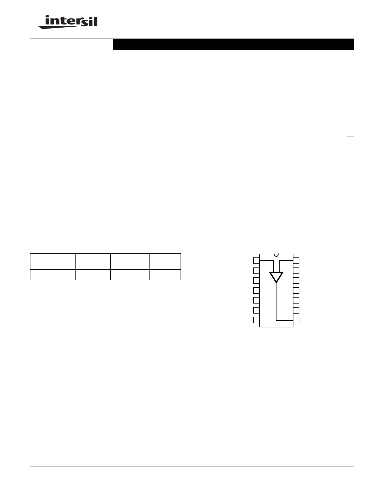
Pinout
HA-2539 (PDIP)
TOP VIEW
PART NUMBER
HA3-2539-5 0 to 75 14 Ld PDIP E14.3
TEMP.
RANGE (oC) PACKAGE PKG. NO.
+IN
1
+
2
NC
3
V-
4
NC
5
NC
6
NC
7
NC
NOTE: No-Connection (NC) leads may be tied to a ground plane
for better isolation and heat dissipation.
14
-IN
-
13
NC
12
NC
11
NC
10
+V
9
NC
8
OUTPUT
1
CAUTION: These devices are sensitive to electrostatic discharge; follow proper IC Handling Procedures.
1-888-INTERSIL or 321-724-7143
| Intersil (and design) is a registered trademark of Intersil Americas Inc.
All other trademarks mentioned are the property of their respective owners.
Copyright © Intersil Americas Inc. 2003. All Rights Reserved
Page 2
HA-2539
www.BDTIC.com/Intersil
Absolute Maximum Ratings Thermal Information
Supply Voltage Between V+ and V- Terminals . . . . . . . . . . . . . 35V
Differential Input Voltage . . . . . . . . . . . . . . . . . . . . . . . . . . . . . . . 6V
Peak Output Current . . . . . . . . . . . . . . . . . . . . . . . . . . . . . . . . 50mA
Continuous Output Current . . . . . . . . . . . . . . . . . . . . . . . 33mA
RMS
Operating Conditions
Temperature Range
HA-2539-5 . . . . . . . . . . . . . . . . . . . . . . . . . . . . . . . . 0
CAUTION: Stresses above those listed in “Absolute Maximum Ratings” may cause permanent damage to the device. This is a stress only rating and operation of the
device at these or any other conditions above those indicated in the operational sections of this specification is not implied.
NOTES:
1. Maximum power dissipation with load conditions must be designed to maintain the maximum junction temperature below 150
package. By using Application Note AN556 on Safe Operating Area equations, along with the thermal resistances, proper load conditions can
be determined. Heat sinking is recommended above 75
2. θJA is measured with the component mounted on a low effective thermal conductivity test board in free air. See Tech Brief TB379 for details.
o
C to 75oC
o
C.
Thermal Resistance (Typical, Note 2) θ
PDIP Package . . . . . . . . . . . . . . . . . . . 95 N/A
Maximum Internal Quiescent Power Dissipation (Note 1)
Maximum Junction Temperature (Plastic Package) . . . . . . . .150
Maximum Storage Temperature Range . . . . . . . . . -65
Maximum Lead Temperature (Soldering 10s). . . . . . . . . . . . 300
(oC/W) θJC (oC/W)
JA
o
C to 150oC
o
C for the plastic
o
o
C
C
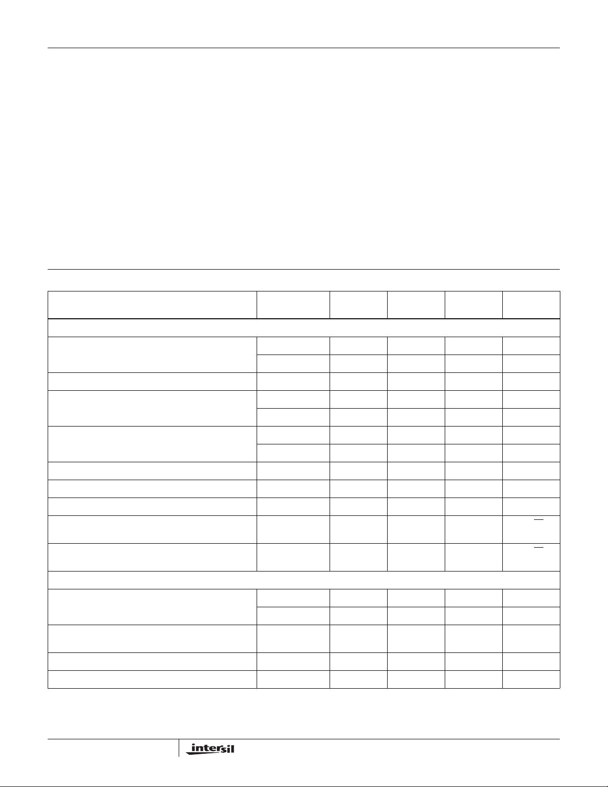
Electrical Specifications V
PARAMETER
INPUT CHARACTERISTICS
Offset Voltage 25 - 8 15 mV
Average Offset Voltage Drift Full - 20 - µV/
Bias Current 25 - 5 20 µA
Offset Current 25 - 1 6 µA
Input Resistance 25 - 10 - kΩ
Input Capacitance 25 - 1 - pF
Common Mode Range Full ±10.0 - - V
Input Current Noise
(f = 1kHz, R
Input Voltage Noise
(f = 1kHz, R
TRANSFER CHARACTERISTICS
SOURCE
SOURCE
= 0Ω)
= 0Ω)
= ±15V, RL = 1kW, CL < 10pF, Unless Otherwise Specified
SUPPLY
TEMP.
o
(
C) MIN TYP MAX UNITS
Full - 13 20 mV
Full - - 25 µA
Full - - 8 µA
25 - 6 - pA/√Hz
25 - 6 - nV/√Hz
o
C
Large Signal Voltage Gain
(Note 3)
Common Mode Rejection Ratio
(Note 4)
Minimum Stable Gain 25 10 - - V/V
Gain Bandwidth (Notes 5, 6) 25 - 600 - MHz
25 10 15 - kV/V
Full 5 - -- kV/V
Full 60 72 - dB
2
Page 3
HA-2539
www.BDTIC.com/Intersil
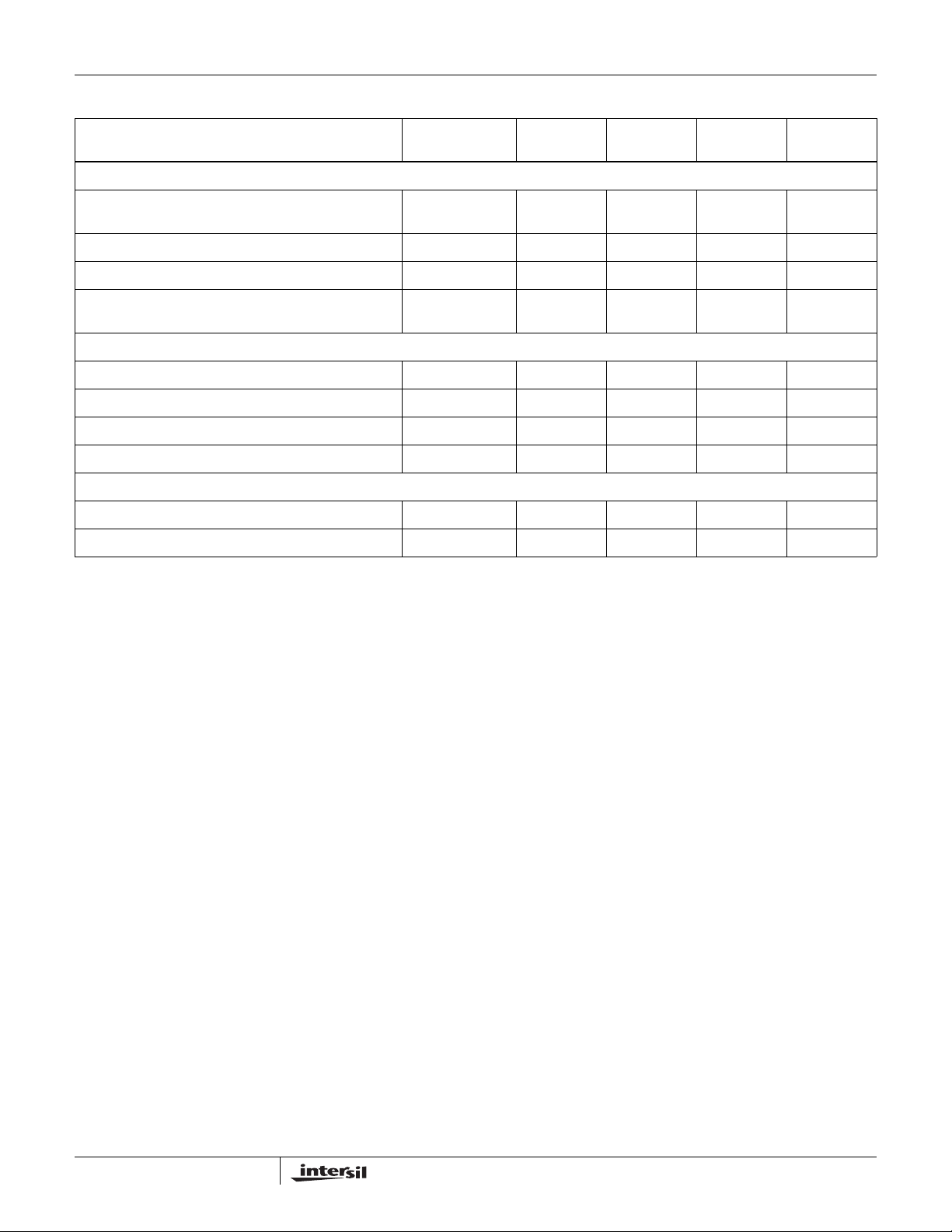
Electrical Specifications V
PARAMETER
OUTPUT CHARACTERISTICS
Output Voltage Swing
(Notes 3, 10)
Output Current (Note 3) 25 ±10 ±20 - mA
Output Resistance 25 - 30 - Ω
Full Power Bandwidth
(Notes 3, 7)
TRANSIENT RESPONSE (Note 8)
Rise Time 25 - 7 - ns
Overshoot 25 - 15 - %
Slew R a t e 25 550 600 - V/µs
Settling Time: 10V Step to 0.1% 25 - 180 - ns
POWER REQUIREMENTS
Supply Current Full - 20 25 mA
Power Supply Rejection Ratio (Note 9) Full 60 70 - dB
= ±15V, RL = 1kW, CL < 10pF, Unless Otherwise Specified (Continued)
SUPPLY
TEMP.
o
(
C) MIN TYP MAX UNITS
Full ±10.0 - - V
25 8.7 9.5 - MHz
NOTES:
= 1kΩ, VO = ±10V.
3. R
L
= ±10.0V.
4. V
CM
= 90mV.
5. V
O
6. A
= 10.
V
7. Full Power Bandwidth guaranteed based on slew rate measurement using: .
8. Refer to Test Circuits section of data sheet.
9. V
10. Guaranteed range for output voltage is ±10V. Functional operation outside of this range is not guaranteed.
= +5V, -15V and +15V, -5V.
SUPPLY
FPBW
Slew Rate
---------------------------- -=
2π V
PEAK
3
Page 4

Test Circuits and Waveforms
www.BDTIC.com/Intersil
HA-2539
IN
A
B
+
900Ω
100Ω
FIGURE 1. TEST CIRCUIT
OUT
NOTES:
11. V
12. A
13. C
= ±15V.
S
= +10.
V
≤ 10pF.
L
Vertical Scale: A = 0.5V/Div., B = 5.0V/Div.
Horizontal Scale: 50ns/Div.
FIGURE 2. LARGE SIGNAL RESPONSE FIGURE 3. SMALL SIGNAL RESPONSE
0.001µF
V+
INPUT
200Ω
500Ω
SETTLE
POINT
1µF
-
+
0.001µF
V-
1µF
2kΩ
5kΩ
Vertical Scale: Input = 10mV/Div., Output = 50mV/Div.
Horizontal Scale: 20ns/Div.
NOTES:
14. A
= -10.
V
15. Load Capacitance should be less than 10pF.
OUTPUT
<10pF
PROBE
MONITOR
FIGURE 4. SETTLING TIME CIRCUIT
16. It is recommended that resistors be carbon composition and that
feedback and summing network ratios be matched to 0.1%.
17. SETTLE POINT (Summing Node) capacitance should be less
than 10pF. For optimum settling time results, it is recommended
that the test circuit be constructed directly onto the device pins.
A Tektronix 568 Sampling Oscilloscope with S-3A sampling
heads is recommended as a settle point monitor.
4
Page 5

Schematic Diagram
www.BDTIC.com/Intersil
R
23
Q
P22
R
R
22
+INPUT
Q
P23
-INPUT
Z
1
R
D
Z1
HA-2539
V+
R
N7
4
Q
P6
Q
N9
Q
P8
Q
N10
Q
N16
R
18
OUTPUT
R
19
Q
P11
R
24
25
Q
N14
R
1
2
Q
P18
Q
V-
Q
N21
R
21
V+
Q
N20
P19
Q
P28
Q
R
13
Q
P25
V-
V+
Q
N25
R
Q
N1
R
6
R
8
Q
P3
10
P17
R
3
R
5
Q
P5
C
Q
N2
R
7
R
9
Q
P4
Q
N15
1
R
Q
Q
N12
R
16
Q
N13
D
Z2
R
R
11
12
Q
N29
R
14
R
15
R
17
V-
5
Page 6

Typical Applications
www.BDTIC.com/Intersil
20 - 100pF
20Ω
+
-
SET A
HA-2539
HA-2539
R
1
= 1+
V
R
1
R
2
= 5
R
2
R
1
-
+
SET AV =
R
2
Z
IN
-R
2
= -3
R
1
FIGURE 5. FREQUENCY COMPENSATION BY OVERDAMPING FIGURE 6. STABILIZATION USING Z
R5 1kΩ R4 10kΩ
INPUT
10kΩ
R
1
3900pF
C
1
-
+
HA-5170
0.039µF
C
2
1kΩ
R
2
R
3
1kΩ
HA-2539
-
+
OUTPUT
IN
FIGURE 7. REDUCING DC ERRORS; COMPOSITE AMPLIFIER FIGURE 8. DIFFERENTIAL GAIN ERROR (3%) HA-2539 20dB
VIDEO GAIN BLOCK
Typical Performance Curves
14
12
10
8
6
4
INPUT BIAS CURRENT (µA)
2
0
-80 -40 0 40 80 120 160
OFFSET VOLTAGE
BIAS CURRENT
TEMPERATURE (
o
C)
FIGURE 9. INPUT OFFSET VOLTAGE AND BIAS CURRENT vs
TEMPERATURE
7
R
6
5
4
3
2
| OFFSET VOLTAGE (mV)
IO
|V
1
0
25
20
15
10
5
NOISE VOLTAGE (nV/√Hz)
VOLTAGE NOISE
0
10 100 1K 10K 100K
= 0Ω
SOURCE
FREQUENCY (Hz)
VS = ±15V
CURRENT NOISE
50
40
30
20
10
0
FIGURE 10. INPUT NOISE VOLTAGE AND NOISE CURRENT vs
FREQUENCY
)
NOISE CURRENT (pA/√Hz
6
Page 7

Typical Performance Curves (Continued)
www.BDTIC.com/Intersil
+40µV
+30µV
+20µV
HA-2539
100
+10µV
0µV
-10µV
-20µV
-30µV
-40µV
Vertical Scale: 10mV/Div.
Horizontal Scale: 50ms/Div.
80
60
CMRR (dB)
40
20
0
1K 10K 100K 1M 10M
FREQUENCY (Hz)
FIGURE 11. BROADBAND NOISE (0.1Hz TO 1MHz) FIGURE 12. COMMON MODE REJECTION RATIO vs
FREQUENCY
100
100
80
60
PSRR (dB)
40
20
80
60
40
GAIN (dB)
20
PHASE
0
GAIN
0
45
90
135
180
PHASE (DEGREES)
0
1K 10K 100K 1M 10M
FREQUENCY (Hz)
FIGURE 13. POWER SUPPLY REJECTION RATIO vs
-20
1K 10K 100K 1M 10M100 100M
FREQUENCY (Hz)
FIGURE 14. OPEN LOOP GAIN/PHASE vs FREQUENCY
FREQUENCY
28
100
VS = ±15V
90
80
70
60
50
40
30
20
CLOSED LOOP GAIN (dB)
10
0
-10
1K 10K 100K 1M 10M100 100M
FREQUENCY (Hz)
24
)
P-P
20
16
12
8
OUTPUT VOLTAGE (V
4
0
1K 10K 100K 1M 10M 100M
VS = ±15V
VS = ±10V
VS = ±5V
FREQUENCY (Hz)
FIGURE 15. CLOSED LOOP FREQUENCY RESPONSE FIGURE 16. OUTPUT VOLTAGE SWING vs FREQUENCY
225
7
Page 8

Typical Performance Curves (Continued)
www.BDTIC.com/Intersil
HA-2539
1.4
28
)
24
P-P
20
16
12
8
4
OUTPUT VOLTAGE SWING (V
0
0 200 400 600 800 1K 1.2K
RESISTANCE (Ω)
1.3
C
o
1.2
1.1
1.0
0.9
0.8
NORMALIZED PARAMETERS
REFERRED TO VALUES AT 25
0.7
0.6
-80 -40 0 40 80 120 160
BANDWIDTH
TEMPERATURE (
o
C)
SLEW RATE
FIGURE 17. OUTPUT VOLTAGE SWING vs LOAD RESISTANCE FIGURE 18 . NORMALIZED A C PARAMETE RS vs TEMPE RATUR E
28
10
8
6
4
2
0
-2
-4
-6
-8
OUTPUT VOLTAGE STEP (V)
-10
10mV
10mV
1mV
1mV
24
20
16
12
SUPPLY CURRENT (mA)
VS = ±15V
VS = ±5V
8
4
0 40 80 120 160 200 240
SETTLING TIME (ns)
FIGURE 19. SETTLING TIME FOR VARIOUS OUTPUT STEP
VOLTAGES
0
-80 -40 0 40 80 120 160
TEMPERATURE (
o
C)
FIGURE 20. POWER SUPPLY CURRENT vs TEMPERATURE
8
Page 9

Die Characteristics
www.BDTIC.com/Intersil
HA-2539
DIE DIMENSIONS:
62 mils x 76 mils x 19 mils
1575µm x 1930µm x 483µm
METALLIZATION:
Type: Al, 1% Cu
Thickness: 16kÅ ±2kÅ
PASSIVATION:
Type: Nitride (Si
Silox Thickness: 12k
Nitride Thickness: 3.5kÅ ±1.5kÅ
) over Silox (SiO2, 5% Phos.)
3N4
Å ±2kÅ
Metallization Mask Layout
V-
SUBSTRATE POTENTIAL (POWERED UP):
V-
TRANSISTOR COUNT:
30
PROCESS:
Bipolar Dielectric Isolation
+IN
OUTPUT
V+
-IN
9
Page 10

Dual-In-Line Plastic Packages (PDIP)
www.BDTIC.com/Intersil
HA-2539
N
D1
-C-
E1
-B-
A1
A2
E
A
L
e
C
C
L
e
A
C
e
B
INDEX
AREA
BASE
PLANE
SEATING
PLANE
NOTES:
1. Controlling Dimensions: INCH. In case of conflict between English
and Metric dimensions, the inch dimensions control.
2. Dimensioning and tolerancing per ANSI Y14.5M-1982.
3. Symbols are defined in the “MO Series Symbol List” in Section 2.2 of
Publication No. 95.
4. Dimensions A, A1 and L are measured with the package seated in
JEDEC seating plane gauge GS-3.
5. D, D1, and E1 dimensions do not include mold flash or protrusions.
Mold flash or protrusions shall not exceed 0.010 inch (0.25mm).
6. E and are measured with the leads constrained to be perpendicular to datum .
7. e
strained. e
8. B1 maximum dimensions do not include dambar protrusions. Dambar
protrusions shall not exceed 0.010 inch (0.25mm).
9. N is the maximum number of terminal positions.
10. Corner leads (1, N, N/2 and N/2 + 1) for E8.3, E16.3, E18.3, E28.3,
E42.6 will have a B1 dimension of 0.030 - 0.045 inch (0.76 -
1.14mm).
12 3 N/2
-A-
D1
B1
B
e
A
and eC are measured at the lead tips with the leads uncon-
B
D
e
0.010 (0.25) C AM BS
-C-
must be zero or greater.
C
E14.3 (JEDEC MS-001-AA ISSUE D)
14 LEAD DUAL-IN-LINE PLASTIC PACKAGE
INCHES MILLIMETERS
SYMBOL
A - 0.210 - 5.33 4
A1 0.015 - 0.39 - 4
A2 0.115 0.195 2.93 4.95 -
B 0.014 0.022 0.356 0.558 B1 0.045 0.070 1.15 1.77 8
C 0.008 0.014 0.204 0.355 -
D 0.735 0.775 18.66 19.68 5
D1 0.005 - 0.13 - 5
E 0.300 0.325 7.62 8.25 6
E1 0.240 0.280 6.10 7.11 5
e 0.100 BSC 2.54 BSC -
e
A
e
B
L 0.115 0.150 2.93 3.81 4
N14 149
0.300 BSC 7.62 BSC 6
- 0.430 - 10.92 7
NOTESMIN MAX MIN MAX
Rev. 0 12/93
All Intersil U.S. products are manufactured, assembled and tested utilizing ISO9000 quality systems.
Intersil Corporation’s quality certifications can be viewed at www.intersil.com/design/quality
Intersil products are sold by description only. Intersil Corporation reserves the right to make changes in circuit design, software and/or specifications at any time without
notice. Accordingly, the reader is ca utioned to verify that data she ets are current before pl acing orders. Information fur nished by Intersil is believed to be accurate and
reliable. However, no responsibility is assumed by Intersil or its subsidiaries for its use; nor for any infringements of patents or other rights of third parties which may result
from its use. No license is granted by implication or othe rwise under any patent or patent rights of Intersil or its subsidia ries.
For information regarding Intersil Corporation and its products, see www.intersil.com
10
 Loading...