


查询EL5203IS-T13供应商
®
EL5102, EL5103, EL5202, EL5203, EL5302
Data Sheet October 3, 2005
400MHz Slew Enhanced VFAs
The EL5x02 and EL5x03 families represent high-speed
VFAs based on a CFA amplifier architecture. This gives the
typical high slew rate benefits of a CFA family along with the
stability and ease of use associated with the VFA type
architecture. With slew rates of 3500V/µs this family of
devices enables the use of voltage feedback amplifiers in a
space where the only alternative has been current feedback
amplifiers. This family will also be available in single, dual,
and triple versions, with 200MHz, 400MHz, and 750MHz
versions. These are all available in single, dual, and triple
versions.
Both families operate on single 5V or ±5V supplies from
minimum supply current. EL5x02 also features an output
enable function, which can be used to put the output in to a
high-impedance mode. This enables the outputs of multiple
amplifiers to be tied together for use in multiplexing
applications.
Typical applications for these families will include cable
driving, filtering, A-to-D and D-to-A buffering, multiplexing
and summing within video, communications, and
instrumentation designs.
FN7331.4
Features
• Operates off 3V, 5V, or ±5V applications
• Power-down to 0µA (EL5x02)
• -3dB bandwidth = 400MHz
• ±0.1dB bandwidth = 50MHz
• Low supply current = 5mA
• Slew rate = 3500V/µs
• Low offset voltage = 5mV max
• Output current = 140mA
VOL
= 2000
•A
• Diff gain/phase = 0.01%/0.01°
• Pb-Free plus anneal available (RoHS compliant)
Applications
• Video amplifiers
• PCMCIA applications
•A/D drivers
• Line drivers
• Portable computers
• High speed communications
• RGB applications
• Broadcast equipment
• Active filtering
1
CAUTION: These devices are sensitive to electrostatic discharge; follow proper IC Handling Procedures.
1-888-INTERSIL or 321-724-7143
| Intersil (and design) is a registered trademark of Intersil Americas Inc.
Copyright © Intersil Americas Inc. 2002-2005. All Rights Reserved.
All other trademarks mentioned are the property of their respective owners.
EL5102, EL5103, EL5202, EL5203, EL5302
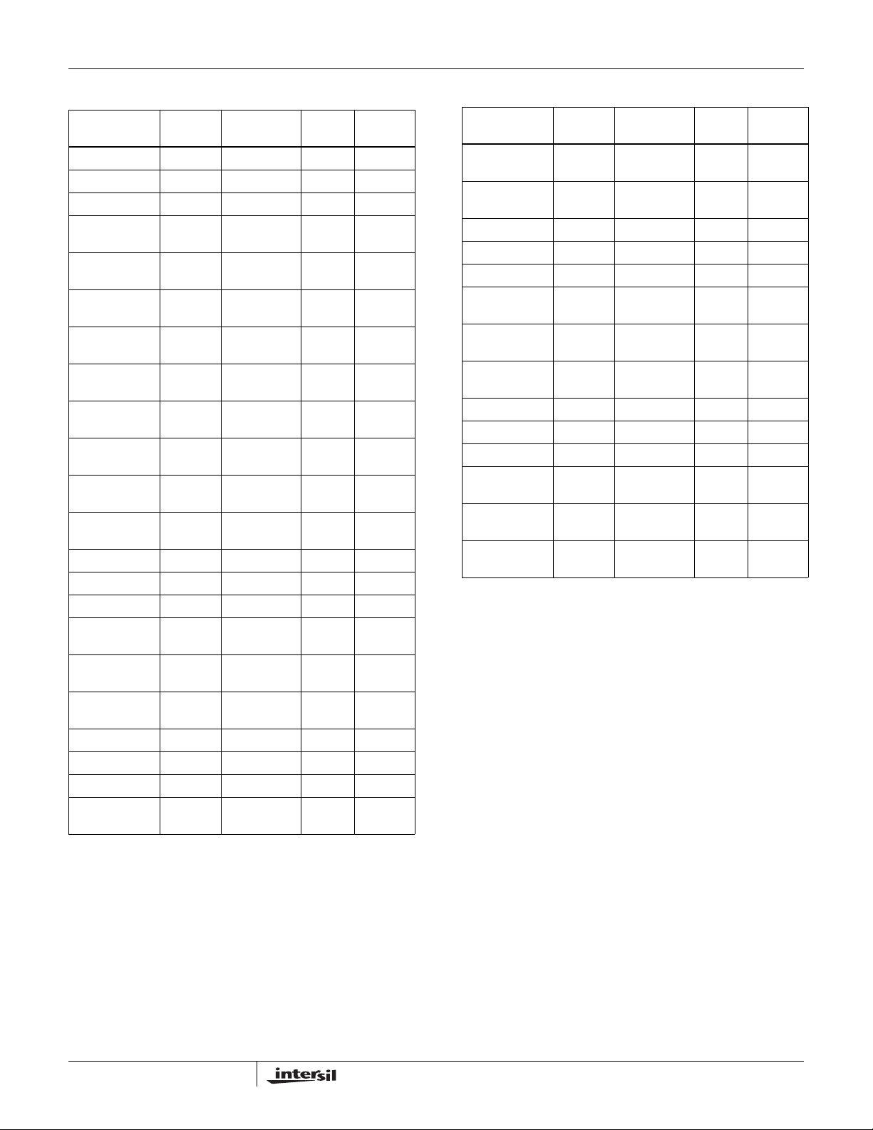
Ordering Information
PART
PART NUMBER
EL5102IS 5102IS 8 Ld SO - MDP0027
EL5102IS-T7 5102IS 8 Ld SO 7” MDP0027
EL5102IS-T13 5102IS 8 Ld SO 13” MDP0027
EL5102ISZ
(See Note)
EL5102ISZ-T7
(See Note)
EL5102ISZ-T13
(See Note)
EL5102IW-T7 q 6 Ld SOT-23 7”
EL5102IW-T7A q 6 Ld SOT-23 7”
EL5103IC-T7 B 5 Ld SC-70 7”
EL5103IC-T7A B 5 Ld SC-70 7”
EL5103IW-T7 g 5 Ld SOT-23 7”
EL5103IW-T7A g 5 Ld SOT-23 7”
EL5202IY BRAAA 10 Ld MSOP - MDP0043
EL5202IY-T7 BRAAA 10 Ld MSOP 7” MDP0043
EL5202IY-T13 BRAAA 10 Ld MSOP 13” MDP0043
EL5202IYZ
(See Note)
EL5202IYZ-T7
(See Note)
EL5202IYZ-T13
(See Note)
EL5203IS 5203IS 8 Ld SO - MDP0027
EL5203IS-T7 5203IS 8 Ld SO 7” MDP0027
EL5203IS-T13 5203IS 8 Ld SO 13” MDP0027
EL5203ISZ
(See Note)
MARKING PACKAGE
5102ISZ 8 Ld SO
(Pb-free)
5102ISZ 8 Ld SO
(Pb-free)
5102ISZ 8 Ld SO
(Pb-free)
BAAAD 10 Ld MSOP
(Pb-free)
BAAAD 10 Ld MSOP
(Pb-free)
BAAAD 10 Ld MSOP
(Pb-free)
5203ISZ 8 Ld SO
(Pb-free)
TAPE &
REEL
13” MDP0027
(3K pcs)
(250 pcs)
(3K pcs)
(250 pcs)
(3K pcs)
(250 pcs)
13” MDP0043
DWG. #
- MDP0027
7” MDP0027
MDP0038
MDP0038
P5.049
P5.049
MDP0038
MDP0038
- MDP0043
7” MDP0043
- MDP0027
PKG.
Ordering Information (Continued)
PART
PART NUMBER
EL5203ISZ-T7
(See Note)
EL5203ISZ-T13
(See Note)
EL5203IY BSAAA 8 Ld MSOP - MDP0043
EL5203IY-T7 BSAAA 8 Ld MSOP 7” MDP0043
EL5203IY-T13 BSAAA 8 Ld MSOP 13” MDP0043
EL5203IYZ
(See Note)
EL5203IYZ-T7
(See Note)
EL5203IYZ-T13
(See Note)
EL5302IU 5302IU 16 Ld QSOP - MDP0040
EL5302IU-T7 5302IU 16 Ld QSOP 7” MDP0040
EL5302IU-T13 5302IU 16 Ld QSOP 13” MDP0040
EL5302IUZ
(See Note)
EL5302IUZ-T7
(See Note)
EL5302IUZ-T13
(See Note)
NOTE: Intersil Pb-free products employ special Pb-free material sets;
molding compounds/die attach materials and 100% matte tin plate
termination finish, which are RoHS compliant and compatible with both
SnPb and Pb-free soldering operations. Intersil Pb-free products are
MSL classified at Pb-free peak reflow temperatures that meet or
exceed the Pb-free requirements of IPC/JEDEC J STD-020.
MARKING PACKAGE
5203ISZ 8 Ld SO
(Pb-free)
5203ISZ 8 Ld SO
(Pb-free)
BAAAE 8 Ld MSOP
(Pb-free)
BAAAE 8 Ld MSOP
(Pb-free)
BAAAE 8 Ld MSOP
(Pb-free)
5302IUZ 16 Ld QSOP
(Pb-free)
5302IUZ 16 Ld QSOP
(Pb-free)
5302IUZ 16 Ld QSOP
(Pb-free)
TAPE &
REEL
7” MDP0027
13” MDP0027
- MDP0043
7” MDP0043
13” MDP0043
- MDP0040
7” MDP0040
13” MDP0040
PKG.
DWG. #
2
FN7331.4
October 3, 2005
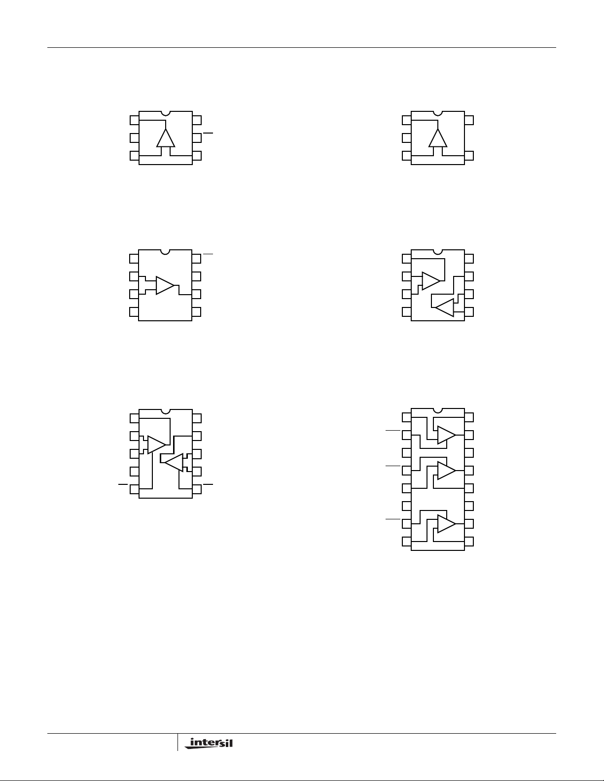
Pinouts
EL5102
(6 LD SOT-23)
TOP VIEW
EL5102, EL5103, EL5202, EL5203, EL5302
EL5103
(5 LD SOT-23)
TOP VIEW
OUT
VS-
IN+
NC
IN-
IN+
VS-
1
2
+-
3
EL5102
(8 LD SO)
TOP VIEW
1
2
-
+
3
4
EL5202
(10 LD MSOP)
TOP VIEW
6
VS+
CE
5
4
IN-
VS-
1
2
3
5
VS+OUT
-+
IN-IN+
4
EL5203
(8 LD SO, MSOP)
TOP VIEW
8
CE
7
VS+
OUT
6
NC
5
OUTA
INA-
INA+
VS-
1
2
+
3
4
VS+
8
OUTB
7
INB-
6
INB+
+
5
EL5302
(16 LD QSOP)
TOP VIEW
1
OUT
2
IN-
IN+
VS-
CE CE
+
3
4
5 6
10
+
1
VS+
OUT
9
IN-
8
IN+
7
7
INA+
CEA
2
3
VS-
CEB
4
INB+
5
NC
6
CEC
7
8 9
INC+
16
INA-
-
+
+
-
+
-
15
14
13
12
11
10
OUTA
VS+
OUTB
INB-
NC
OUTC
INC-
3
FN7331.4
October 3, 2005
EL5102, EL5103, EL5202, EL5203, EL5302
Absolute Maximum Ratings (T
Supply Voltage between V
Maximum Supply Slewrate between V
Input Voltage . . . . . . . . . . . . . . . . . . . . . . . . . . . . . . . . . . . . . . . ±V
Differential Input Voltage . . . . . . . . . . . . . . . . . . . . . . . . . . . . . . .±4V
Maximum Continuous Output Current . . . . . . . . . . . . . . . . . . . 80mA
CAUTION: Stresses above those listed in “Absolute Maximum Ratings” may cause permanent damage to the device. This is a stress only rating and operation of the
device at these or any other conditions above those indicated in the operational sections of this specification is not implied.
IMPORTANT NOTE: All parameters having Min/Max specifications are guaranteed. Typical values are for information purposes only. Unless otherwise noted, all tests
are at the specified temperature and are pulsed tests, therefore: T
+ and GND . . . . . . . . . . . . . . . . . 13.2V
S
DC Electrical Specifications V
= 25°C)
A
+ and VS- . . . . . . . . . 1V/µs
S
J
= +5V, VS- = -5V, TA = 25°C, RL = 500Ω, V
S+
= TC = T
S
A
Maximum Current into I
Power Dissipation . . . . . . . . . . . . . . . . . . . . . . . . . . . . . See Curves
+, IN-, CE . . . . . . . . . . . . . . . . . . . . . ±5mA
N
Storage Temperature Range. . . . . . . . . . . . . . . . . .-65°C to +150°C
Ambient Operating Temperature Range . . . . . . . . . .-40°C to +85°C
Operating Junction Temperature. . . . . . . . . . . . . . . . . . . . . . . 150°C
ENABLE
= +5V, unless otherwise specified.
PARAMETER DESCRIPTION CONDITIONS MIN TYP MAX UNIT
V
OS
Offset Voltage EL5102, EL5103, EL5202, EL5203 1 5 mV
EL5302 2 8 mV
TCV
OS
IB Input Bias Current V
I
OS
TCI
OS
Offset Voltage Temperature Coefficient Measured from T
= 0V -12 2 12 µA
IN
Input Offset Current V
Input Bias Current Temperature
= 0V -8 1 8 µA
IN
Measured from T
MIN
MIN
to T
to T
MAX
MAX
10 µV/°C
50 nA/°C
Coefficient
PSRR Power Supply Rejection Ratio V
CMRR Common Mode Rejection Ratio V
= ±4.75V to ±5.25V -70 -80 dB
S
= -3V to 3.0V -60 -80 dB
CM
CMIR Common Mode Input Range Guaranteed by CMRR test -3 ±3.3 3 V
R
IN
C
IN
I
S,ON
I
S,OFF
AVOL Open Loop Gain V
V
OUT
I
OUT
V
-ON CE Pin Voltage for Power-up (VS+)-5 (VS+)-3 V
CE
V
-OFF CE Pin Voltage for Shut-down (VS+)-1 VS+V
CE
I
-ON Pin Current - Enabled CE = 0V -1 0 +1 µA
EN
I
-OFF Pin Current - Disabled CE = +5V 1 14 25 µA
EN
Input Resistance Common mode 200 400 kΩ
Input Capacitance SO package 1 pF
Supply Current - Enabled per amplifier 4.6 5.2 5.8 mA
Supply Current - Shut-down per amplifier VS++10+25µA
V
--257-1µA
S
= ±2.5V, RL = 1kΩ to GND 58 66 dB
OUT
V
= ±2.5V, RL = 150Ω to GND 60 dB
OUT
Output Voltage Swing RL = 1kΩ to GND ±3.5 ±3.9 V
R
= 150Ω to GND ±3.4 ±3.7 V
L
Output Current AV = 1, RL = 10Ω to 0V ±80 ±150 mA
4
FN7331.4
October 3, 2005

EL5102, EL5103, EL5202, EL5203, EL5302
Closed Loop AC Electrical Specifications V
PARAMETER DESCRIPTION CONDITIONS MIN TYP MAX UNIT
= +5V, VS- = -5V, TA = 25°C, V
S+
ENABLE
GND pin, unless otherwise specified. (Note 1)
= +5V, AV = +1, RF = 0Ω, RL = 150Ω to
BW -3dB Bandwidth (V
SR Slew Rate A
t
R,tF
Rise Time, Fall Time ±0.1V step 2.8 ns
OUT
= 400mV
)AV = 1, RF = 0Ω 400 MHz
P-P
= +2, RL = 100Ω, V
V
R
= 500Ω, V
L
OUT
= -3V to +3V 4000 V/µs
= -3V to +3V 1100 2200 5000 V/µs
OUT
OS Overshoot ±0.1V step 10 %
t
S
dG Differential Gain (Note 2) A
dP Differential Phase (Note 2) A
e
N
i
N
t
DIS
t
EN
0.1% Settling Time VS = ±5V, RL = 500Ω, AV = 1, V
= 2, RF = 1kΩ 0.01 %
V
= 2, RF = 1kΩ 0.01 °
V
= ±3V 20 ns
OUT
Input Noise Voltage f = 10kHz 12 nV/√Hz
Input Noise Current f = 10kHz 11 pA/√Hz
Disable Time (Note 3) 50 ns
Enable Time (Note 3) 25 ns
NOTES:
1. All AC tests are performed on a “warmed up” part, except slew rate, which is pulse tested.
2. Standard NTSC signal = 286mV
, f = 3.58MHz, as VIN is swept from 0.6V to 1.314V.RL is DC coupled.
P-P
3. Disable/Enable time is defined as the time from when the logic signal is applied to the ENABLE pin to when the supply current has reached half
its final value.
5
FN7331.4
October 3, 2005

EL5102, EL5103, EL5202, EL5203, EL5302
Typical Performance Curves
5
V
=±5V
S
4
=+1
A
V
R
=0
F
3
=500Ω
R
L
2
C
=+3.3pF
L
1
0
-1
-2
-3
NORMALIZED GAIN (dB)
-4
-5
0.1 1 10 100 1000
-3dB BW @ 438MHz
FREQUENCY (MHz)
240
VS=±5V
=+1
A
180
V
=0
R
F
=500Ω
R
120
L
C
=+3.3pF
L
60
0
PHASE (°)
-60
-120
-180
-240
0.1 1 10 100 1000
FREQUENCY (MHz)
FIGURE 1. GAIN vs FREQUENCY (-3dB BANDWIDTH) FIGURE 2. PHASE vs FREQUENCY
0.5
VS=±5V
0.4
=+1
A
V
0.3
R
=0
F
=500Ω
R
L
0.2
=+3.3pF
C
L
0.1
0
-0.1
-0.2
-0.3
NORMALIZED GAIN (dB)
-0.4
-0.5
1 10 100
FREQUENCY (MHz)
0.1dB BW @ 35MHz
70
V
=±5V
S
=500Ω
R
60
50
40
GAIN (dB)
30
20
L
GAIN=40dB or 100
FREQ.=1.64 MHz
GAIN BW PRODUCT=1.64x100=164MHz
0 1 10 100
FREQUENCY (MHz)
FIGURE 3. 0.1dB BANDWIDTH FIGURE 4. GAIN BANDWIDTH PRODUCT
300
VS=±5V
R
=500Ω
L
250
200
150
100
GAIN-BANDWIDTH PRODUCT (MHz)
50
2.0 2.5 3.0 3.5 4.0 4.5 5.0 5.5 6.0
SUPPLY VOLTAGES (±V)
FIGURE 5. GAIN BANDWIDTH PRODUCT vs SUPPLY
VOLTAGES
5
VS=±5V
4
R
=500Ω
L
=+3.3pF
C
L
3
2
1
0
-1
-2
-3
NORMALIZED GAIN (dB)
-4
-5
0.1 1 10 100 1000
AV=+5
=1.6K, RG=400
R
F
FREQUENCY (MHz)
AV=+2
R
F=RG
=400Ω
AV=+1
R
=0
F
FIGURE 6. GAIN vs FREQUENCY FOR VARIOUS +A
V
6
FN7331.4
October 3, 2005

EL5102, EL5103, EL5202, EL5203, EL5302
Typical Performance Curves (Continued)
5
AV=+1
4
=0
R
F
=500Ω
R
3
L
C
=+3.3pF
L
2
1
0
-1
-2
-3
NORMALIZED GAIN (dB)
-4
-5
0.1 1 10 100 1000
FREQUENCY (MHz)
VS=±6
VS=±5V
VS=±4V
VS=±3V
VS=±2.5V
FIGURE 7. GAIN vs FREQUENCY FOR VARIOUS ±V
5
VS=±5V
4
=+2
A
V
=402Ω
R
3
F
C
=+3.9pF
L
2
1
0
-1
-2
-3
NORMALIZED GAIN (dB)
-4
-5
0.1 10 100 1000
RL=50Ω
RL=70Ω
R
=150
L
1
FREQUENCY (MHz)
RL=500Ω
RL=1kΩ
Ω
FIGURE 9. GAIN vs FREQUENCY FOR VARIOUS
R
(AV = +2)
LOAD
5
VS=±5V
4
=+1
A
V
=0
R
3
F
C
=+3.3pF
L
2
1
0
-1
-2
-3
NORMALIZED GAIN (dB)
-4
-5
0.1 1 10 100 1000
FREQUENCY (MHz)
S
FIGURE 8. GAIN vs FREQUENCY FOR VARIOUS
R
LOAD (AV
5
V
=±5V
S
4
A
=+5
V
=402Ω
R
3
F
=+3.9pF
C
L
2
1
0
-1
-2
-3
NORMALIZED GAIN (dB)
-4
-5
0.1 1 10 100
= +1)
FREQUENCY (MHz)
RL=500Ω
RL=150Ω
RL=75Ω
RL=50Ω
RL=50Ω
RL=75Ω
RL=150Ω
RL=1kΩ
RL=500Ω
RL=1kΩ
FIGURE 10. GAIN vs FREQUENCY FOR VARIOUS
R
(AV = +5)
LOAD
5
VS=±5V
4
=+1
A
V
=0
R
F
3
=500Ω
R
L
2
1
0
-1
-2
-3
NORMALIZED GAIN (dB)
-4
-5
0.1 1 10 100 1000
FREQUENCY (MHz)
CL=15pF
C
=8.2pF
L
CL=3.3pF
CL=27pF
CL=0pF
FIGURE 11. GAIN vs FREQUENCY FOR VARIOUS
C
(AV =+1)
LOAD
7
5
V
=±5V
S
4
=+2
A
V
=400Ω
R
F
3
R
=500Ω
L
2
1
0
-1
-2
-3
NORMALIZED GAIN (dB)
-4
-5
0.1 1 10 100 1000
CL=33pF
=18pF
C
L
CL=8.2pF
CL=0pF
FREQUENCY (MHz)
CL=47pF
FIGURE 12. GAIN vs FREQUENCY FOR VARIOUS
C
(AV = +2)
LOAD
FN7331.4
October 3, 2005

EL5102, EL5103, EL5202, EL5203, EL5302
Typical Performance Curves (Continued)
5
V
=±5V
S
4
=+5
A
V
R
=400Ω
3
F
=500Ω
R
L
2
1
0
-1
-2
-3
NORMALIZED GAIN (dB)
-4
-5
0.1 1 10 100
CL=150pF
=100pF
C
L
CL=56pF
CL=0pF
FREQUENCY (MHz)
CL=220pF
FIGURE 13. GAIN vs FREQUENCY FOR VARIOUS
C
(AV =+5)
LOAD
5
=±5V
V
S
4
=+2
A
V
=500Ω
R
L
3
=+8pF
C
L
2
1
0
-1
-2
-3
NORMALIZED GAIN (dB)
-4
-5
0.1 1 10 100 1000
RF= 680Ω
RF=402Ω
RF=274Ω
RF=100Ω
FREQUENCY (MHz)
RF=1.0kΩ
5
VS=±5V
4
A
=+1
V
=500Ω
R
L
3
C
=+3pF
L
2
1
0
-1
-2
-3
NORMALIZED GAIN (dB)
-4
-5
0.1 1 10 100 1000
FREQUENCY (MHz)
RF=100Ω
RF=50Ω
RF=150Ω
RF=25Ω
RF=0Ω
FIGURE 14. GAIN vs FREQUENCY FOR VARIOUS R
5
=±5V
V
S
4
=+5
A
V
=500Ω
R
L
3
C
=+12pF
L
2
1
0
-1
-2
-3
NORMALIZED GAIN (dB)
-4
-5
0.1 1 10 100
RF=100Ω
RF=1kΩ
RF=402Ω
FREQUENCY (MHz)
RF=4kΩ
RF=2kΩ
(AV = +1)
F
FIGURE 15. GAIN vs FREQUENCY FOR VARIOUS R
5
V
=±5V
S
4
=+2
A
V
=RG=402Ω
R
3
F
R
=500Ω
L
2
=+8pF
C
L
1
0
-1
-2
-3
NORMALIZED GAIN (dB)
-4
-5
0.1 1 10 100 1000
CIN=3.3pF
CIN=2.2pF
CIN=1pF
FREQUENCY (MHz)
CIN=4.7pF
CIN=0pF
FIGURE 17. GAIN vs FREQUENCY FOR VARIOUS C
(A
= +2)
V
8
(AV = +2) FIGURE 16. GAIN vs FREQUENCY FOR VARIOUS RF (AV = +5)
F
5
=±5V
V
S
4
A
=+5
V
=402Ω
R
3
G
=1600Ω
R
L
2
=+12pF
C
L
1
0
-1
-2
-3
NORMALIZED GAIN (dB)
-4
-5
0.1 1 10 100
(-)
IN
FIGURE 18. GAIN vs FREQUENCY FOR VARIOUS C
(A
FREQUENCY (MHz)
= +5)
V
CIN=8.2pF
CIN=6.8pF
CIN=0pF
C
CIN=4.7pF
IN
=10pF
(-)
IN
FN7331.4
October 3, 2005

EL5102, EL5103, EL5202, EL5203, EL5302
Typical Performance Curves (Continued)
80
70
60
50
40
30
20
GAIN (dB)
10
0
VCC=+5V
-10
-20
=-5V
V
EE
10 100 1K 10K 100K 1M 10M 100M 1G
FREQUENCY (Hz)
GAIN
PHASE
-45
0
45
90
135
180
225
270
315
360
405
PHASE (°)
FIGURE 19. OPEN LOOP GAIN AND PHASE vs FREQUENCY
-10
AV=+5
-20
=±5V
V
S
-30
-40
-50
-60
CMRR (dB)
-70
-80
-90
-100
-110
1K 10K 1M 500M
100K 100M10M
FREQUENCY (Hz)
AV=+2
V
=±5V
S
10
1
0.1
OUTPUT IMPEDANCE (Ω)
0.01
10K 100K 10M 100M
1M
FREQUENCY (Hz)
FIGURE 20. OUTPUT IMPEDANCE/PHASE vs FREQUENCY
10
AV=+1
0
=±5V
V
S
-10
-20
-30
-40
PSRR (dB)
-50
-60
+PSRR
-70
-80
-PSRR
-90
1K 10K 1M 500M
100K
FREQUENCY (Hz)
100M10M
FIGURE 21. CMRR vs FREQUENCY
10
9
8
7
6
5
4
=±5V
V
3
S
=+2
A
V
2
1
0
MAX OUTPUT VOLTAGE SWING (Vp-p)
=402Ω
R
F=RG
=8pF
C
L
0.1 1 10 100 1000
R
LOAD
FREQUENCY (MHz)
=150Ω
R
LOAD
=1kΩ
FIGURE 23. MAX OUTPUT VOLTAGE SWING vs FREQUENCY
9
FIGURE 22. PSRR vs FREQUENCY
30
VS=±5V
25
=+1
A
V
20
=0
R
F
15
=500Ω
R
L
10
5
0
-5
-10
-15
GROUP DELAY (ns)
-20
-25
-30
0.1 1 10 100 1000
FREQUENCY (MHz)
FIGURE 24. GROUP DELAY vs FREQUENCY
FN7331.4
October 3, 2005

EL5102, EL5103, EL5202, EL5203, EL5302
Typical Performance Curves (Continued)
-10
V
=±5V
S
-20
A
=+1
V
=0
R
F
-30
CHIP DISABLED
OUTPUT to INPUT
-40
-50
-60
-70
ISOLATION (dB)
INPUT to OUTPUT
-80
-90
-100
0.1 1 10 100 1000
FREQUENCY (MHz)
FIGURE 25. INPUT AND OUTPUT ISOLATION
-30
V
=±5V
S
=+1
A
-40
V
R
=0
F
=500Ω
R
L
-50
=3.3pF
C
L
=2Vp-p
V
OUT
-60
-70
-80
-90
HARMONIC DISTORTION (dBc)
-100
0.1 1 10 100
FUNDAMENTAL FREQUENCY (MHz)
T.H.D
2nd HD
3rd HD
10
=±5V
V
S
0
A
=+1
V
-10
=0
R
F
-20
R
=500Ω
L
-30
-40
-50
-60
GAIN (dB)
-70
NOTE:
This was done on the
EL5203 (Dual Op-Amps)
B in to A Out
A in to B Out
-80
-90
-100
-110
-120
0.1 1 10 100 1000
FREQUENCY (MHz)
FIGURE 26. CHANNEL TO CHANNEL ISOLATION
-20
=±5V
V
S
A
=+5
-30
V
=402Ω
R
G
-40
=1600Ω
R
F
R
=500Ω
L
-50
=12pF
C
L
-60
-70
THD (dBc)
-80
-90
-100
012345678
FIN=10MHz
FIN=1MHz
OUTPUT VOLTAGES (Vp-p)
FIGURE 27. HARMONIC DISTORTION vs FREQUENCY
6
5
ENABLE SIGNAL
4
3
2
OUTPUT SIGNAL
1
0
AMPLITUDE (V)
-1
-2
-3
-600
-400 -200 0 200 400 600 800 10001200 1400 1600
TIME (ns)
V
A
R
R
V
=±5V
S
=+1
V
=0
F
=500Ω
L
OUT
=2Vp-p
FIGURE 29. TURN-ON TIME
10
FIGURE 28. TOTAL HARMONIC DISTORTION vs OUTPUT
VOLTAGES
6
VS=±5V
A
=+1
5
V
=0
R
F
4
=500
Ω
R
L
V
=2Vp-p
OUT
3
2
DISABLE SIGNAL
OUTPUT SIGNAL
1
0
AMPLITUDE (V)
-1
-2
-3
-600 -400 -200 0 200 400 600 800 1000120014001600
TIME (ns)
FIGURE 30. TURN-OFF TIME
FN7331.4
October 3, 2005

EL5102, EL5103, EL5202, EL5203, EL5302
Typical Performance Curves (Continued)
VS=±5V
100
10
NOISE VOLTAGE (nV/√Hz)
1
10 100 10K 100K
1K
FREQUENCY (Hz)
FIGURE 31. EQUIVALENT NOISE VOLTAGE vs FREQUENCY
5
=±5V
V
S
4
A
V
R
G
3
2
1
0
AMPLITUDE (V)
-1
-2
-3
-20 0 20 40 60 80 100 120 140 160
=+5
=25Ω
T
RISE
R
=500Ω
L
=5pF
C
L
V
OUT
=1.243ns
=4.0V
T
FALL
TIME (ns)
=1.167ns
0.5
=±5V
V
S
A
=+1
0.4
V
=0
R
F
0.3
0.2
0.1
0.0
-0.1
AMPLITUDE (V)
-0.2
-0.3
-20 0 20 40 60 80 100 120 140 160
T
R
L
C
L
V
OUT
RISE
=500Ω
=3.3pF
=400mV
=0.923ns
TIME (ns)
T
FALL
=0.9ns
FIGURE 32. SMALL SIGNAL STEP RESPONSE_RISE AND
FALL TIME
6.0
AV=+1
5.8
=0
R
F
=500Ω
R
L
5.6
=3.3pF
C
L
5.4
5.2
5.0
4.8
4.6
4.4
SUPPLY CURRENT (mA)
4.2
4.0
2.5 3.0 3.5 4.0 4.5 5.0 5.5 6.0
Please note that the curve showed
positive Current. The negative current was almost the same.
SUPPLY VOLTAGE (V)
FIGURE 33. LARGE SIGNAL STEP RESPONSE_RISE AND
FALL TIME
10
=±5V
V
S
0
=+5
A
V
=1600Ω
R
-10
F
=100Ω
R
L
-20
=12pF
C
L
-30
f1=1dBm
-40
@ 0.95MHz
-50
2f1-f2=-76.8dBm
-60
@ 0.85MHz
-70
AMPLITUDE (dBm)
-80
-90
-100
0.8 0.9 1.0 1.1 1.2
FREQUENCY (MHz)
Delta IM=(1)-(-77)=78dB
IP3=1+(78/2)=40dBm
f2=1dBm
@ 1.05MHz
2f2-f1=-77.0dBm
@ 1.15MHz
FIGURE 35. THIRD ORDER IMD INTERCEPT (IP3)
11
FIGURE 34. SUPPLY CURRENT vs SUPPLY VOLTAGE
50
45
40
35
30
25
IP3 (dBm)
20
15
10
5
0
110100
FIGURE 36.
FREQUENCY (MHz)
THIRD ORDER IMD INTERCEPT vs FREQUENCY
VS=±5V
=+5
A
V
=1600Ω
R
F
=100Ω
R
L
=12pF
C
L
FN7331.4
October 3, 2005

EL5102, EL5103, EL5202, EL5203, EL5302
Typical Performance Curves (Continued)
JEDEC JESD51-7 HIGH EFFECTIVE THERMAL
CONDUCTIVITY TEST BOARD
1.2
1.087W
1
0.8
0.6
543mW
0.4
0.2
POWER DISSIPATION (W)
0
0 255075100 150
M
S
O
θ
P
J
A
8
=
/
1
1
1
0
5
°
C
/
W
S
O
T
2
3-
θ
AMBIENT TEMPERATURE (°C)
5/6
J
A
=
230°
C
/W
85
125
FIGURE 37. PACKAGE POWER DISSIPATION vs AMBIENT
TEMPERATURE
JEDEC JESD51-3 LOW EFFECTIVE THERMAL
CONDUCTIVITY TEST BOARD
0.7
607mW
0.6
488mW
0.5
0.4
0.3
0.2
POWER DISSIPATION (W)
0.1
0
SOT23-5/6
θJA=256°C/W
0 255075100 150
AMBIENT TEMPERATURE (°C)
MSOP8/10
θJA=206°C/W
85
125
JEDEC JESD51-7 HIGH EFFECTIVE THERMAL
CONDUCTIVITY TEST BOARD
1.4
1.136W
1.2
1.116W
1
0.8
0.6
0.4
POWER DISSIPATION (W)
0.2
0
0 255075100 150
QSOP16
θJA=112°C/W
AMBIENT TEMPERATURE (°C)
SO8
θJA=110°C/W
12585
FIGURE 38. PACKAGE POWER DISSIPATION vs AMBIENT
TEMPERATURE
JEDEC JESD51-3 LOW EFFECTIVE THERMAL
CONDUCTIVITY TEST BOARD
1
791mW
0.8
781mW
0.6
0.4
0.2
POWER DISSIPATION (W)
0
θJA=160°C/W
0 255075100 150
AMBIENT TEMPERATURE (°C)
QSOP16
θJA=158°C/W
SO8
12585
FIGURE 39. PACKAGE POWER DISSIPATION vs AMBIENT
TEMPERATURE
FIGURE 40. PACKAGE POWER DISSIPATION vs AMBIENT
TEMPERATURE
All Intersil U.S. products are manufactured, assembled and tested utilizing ISO9000 quality systems.
Intersil Corporation’s quality certifications can be viewed at www.intersil.com/design/quality
Intersil products are sold by description only. Intersil Corporation reserves the right to make changes in circuit design, software and/or specifications at any time without
notice. Accordingly, the reader is cautioned to verify that data sheets are current before placing orders. Information furnished by Intersil is believed to be accurate and
reliable. However, no responsibility is assumed by Intersil or its subsidiaries for its use; nor for any infringements of patents or other rights of third parties which may result
from its use. No license is granted by implication or otherwise under any patent or patent rights of Intersil or its subsidiaries.
For information regarding Intersil Corporation and its products, see www.intersil.com
12
FN7331.4
October 3, 2005

Copyright © Each Manufacturing Company.
All Datasheets cannot be modified without permission.
This datasheet has been download from :
www.AllDataSheet.com
100% Free DataSheet Search Site.
Free Download.
No Register.
Fast Search System.
www.AllDataSheet.com
 Loading...