

Page 1
查询EL4543供应商
®
EL4543
Data Sheet October 26, 2005
Triple Differential Twisted-Pair Driver with
Common-Mode Sync Encoding
The EL4543 is a high bandwidth triple differential amplifier
with integrated encoding of video sync signals. The inputs
are suitable for handling high speed video or other
communications signals in either single-ended or differential
form, and the common-mode input range extends all the way
to the negative rail enabling ground-referenced signalling in
single supply applications. The high bandwidth enables
differential signalling onto standard twisted-pair or coax with
very low harmonic distortion, while internal feedback
ensures balanced gain and phase at the outputs reducing
radiated EMI and harmonics.
Embedded logic encodes standard video horizontal and
vertical sync signals onto the common mode of the twisted
pair(s), transmitting this additional information without the
requirement for additional buffers or transmission lines. The
EL4543 enables significant system cost savings when
compared with discrete line driver alternatives.
FN7325.5
Features
• Fully differential inputs, outputs, and feedback
• 350MHz -3dB bandwidth
• 1200V/µs slew rate
• -75dB distortion at 5MHz
• Single 5V to 12V operation
• 50mA minimum output current
• Low power - 36mA total typical supply current
• Pb-free plus anneal available (RoHS compliant)
Applications
• Twisted-pair drivers
• Differential line drivers
• VGA over twisted-pair
• Transmission of analog signals in a noisy environment
The EL4543 is available in a 24 Ld QSOP package and is
specified for operation over the -40°C to +85°C temperature
range.
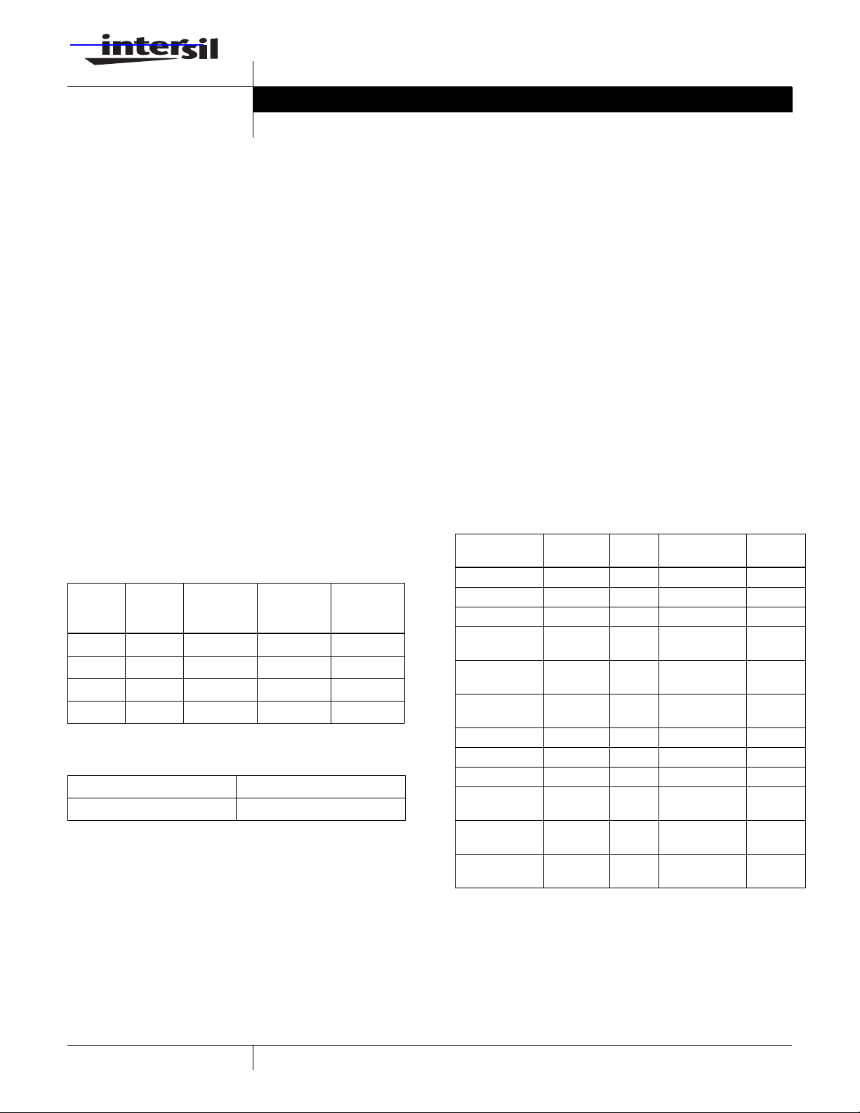
TABLE 1. SYNC SIGNAL ENCODING
COMMON
MODE A
HV
Low High 3.0 2.0 2.5
Low Low 2.5 3.0 2.0
High Low 2.0 3.0 2.5
High High 2.5 2.0 3.0
TABLE 2. INPUT LOGIC THRESHOLD (+5V SUPPLY)
V
, max 0.8V
LO
V
, min 2V
HI
(RED)
COMMON
MODE B
(GREEN)
COMMON
MODE C
(BLUE)
Ordering Information
PART
NUMBER
EL4543IU EL4543IU - 24 Ld QSOP MDP0040
EL4543IU-T7 EL4543IU 7” 24 Ld QSOP MDP0040
EL4543IU-T13 EL4543IU 13” 24 Ld QSOP MDP0040
EL4543IUZ
(See Note)
EL4543IUZ-T7
(See Note)
EL4543IUZ-T13
(See Note)
EL4543IL 4543IL - 20 Ld 4x4 QFN* MDP0046
EL4543IL-T7 4543IL 7” 20 Ld 4x4 QFN* MDP0046
EL4543IL-T13 4543IL 13” 20 Ld 4x4 QFN* MDP0046
EL4543ILZ
(See Note)
EL4543ILZ-T7
(See Note)
EL4543ILZ-T13
(See Note)
NOTE: Intersil Pb-free plus anneal products employ special Pb-free
material sets; molding compounds/die attach materials and 100% matte tin
plate termination finish, which are RoHS compliant and compatible with
both SnPb and Pb-free soldering operations. Intersil Pb-free products are
MSL classified at Pb-free peak reflow temperatures that meet or exceed
the Pb-free requirements of IPC/JEDEC J STD-020.
*20 Ld 4x4 QFN, exposed pad 2.7 x 2.7mm
PAR T
MARKING
EL4543IUZ - 24 Ld QSOP
EL4543IUZ 7” 24 Ld QSOP
EL4543IUZ 13” 24 Ld QSOP
4543ILZ - 20 Ld 4x4 QFN*
4543ILZ 7” 20 Ld 4x4 QFN*
4543ILZ 13” 20 Ld 4x4 QFN*
TAPE &
REEL PACKAGE
(Pb-Free)
(Pb-Free)
(Pb-Free)
(Pb-Free)
(Pb-Free)
(Pb-Free)
PKG.
DWG. #
MDP0040
MDP0040
MDP0040
MDP0046
MDP0046
MDP0046
1
CAUTION: These devices are sensitive to electrostatic discharge; follow proper IC Handling Procedures.
1-888-INTERSIL or 1-888-468-3774
| Intersil (and design) is a registered trademark of Intersil Americas Inc.
Copyright © Intersil Americas Inc. 2004, 2005. All Rights Reserved.
All other trademarks mentioned are the property of their respective owners.
Page 2
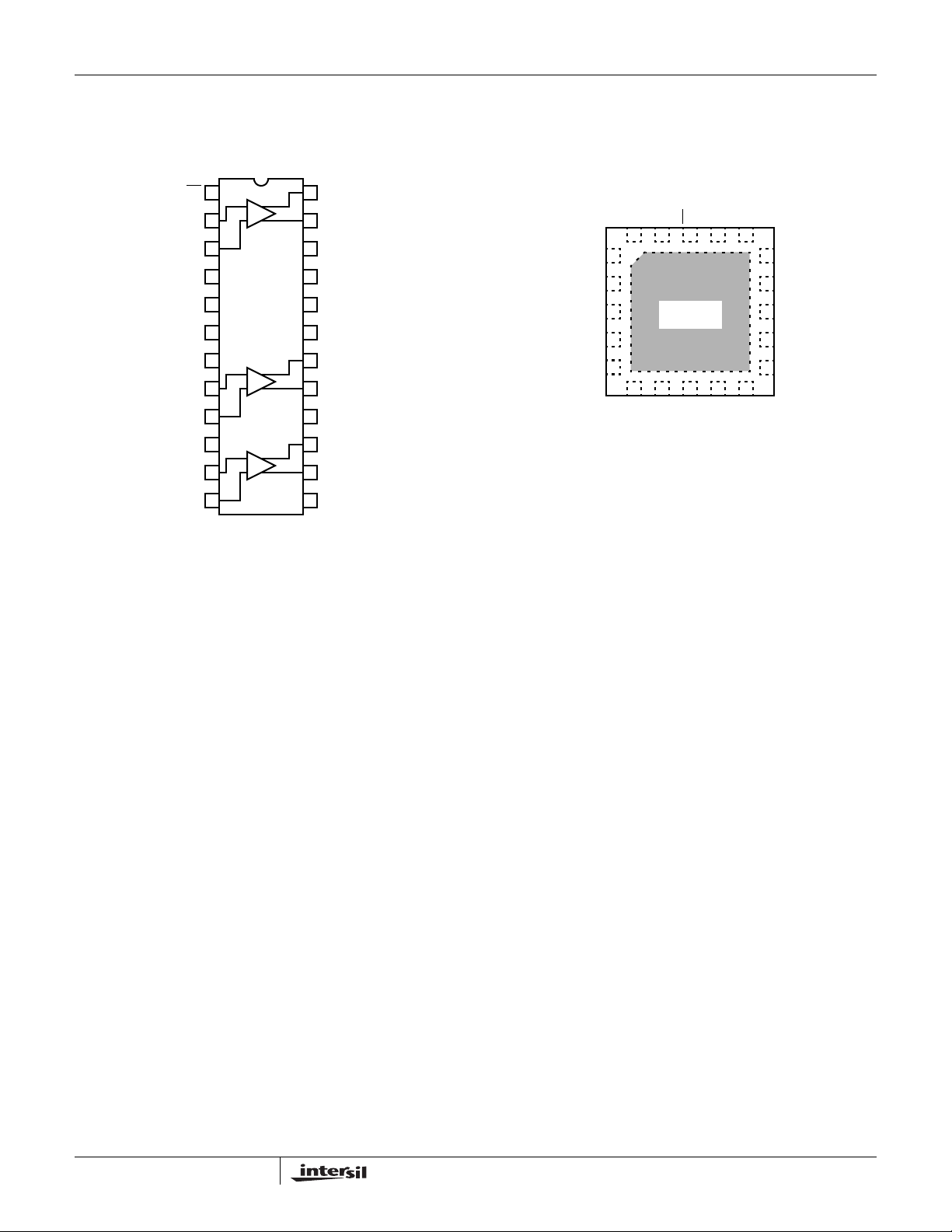
Pinouts
EL4543
(24 LD QSOP)
TOP VIEW
EL4543
EL4543
(20 LD QFN)
TOP VIEW
EN
VINA+
VINA-
NC
VSYNC
HSYNC
NC
VINB+
VINB-
NC
VINC+
VINC-
1
+
2
-
3
4
5
6
7
+
8
-
9
10
+
11
-
12
24
23
22
21
20
19
18
17
16
15
14
13
VOUTA+
VOUTA-
NC
VS+
VS-
NC
VOUTB+
VOUTB-
NC
VOUTC+
VOUTC-
NC
VSYNC
HSYNC
NC
VINB+
VINB-
PAD
EN
18
8
NC
VOUTA+
17
16 VOUTA-
9
10VOUTC+
VOUTC-
15
VS+
VS-
14
NC
13
VOUTB+
12
11 VOUTB-
VINA-
VINA+
20
19
1
2
6
VINC+
THERMAL
7
VINC-
3
4
5
2
FN7325.5
October 26, 2005
Page 3
EL4543
Absolute Maximum Ratings (T
Supply Voltage (V
Maximum Output Continuous Current . . . . . . . . . . . . . . . . . . ±70mA
Storage Temperature Range . . . . . . . . . . . . . . . . . .-65°C to +150°C
+ & VS-). . . . . . . . . . . . . . . . . . . . . . . . . . . .+12V
S
= 25°C)
A
Ambient Operating Temperature . . . . . . . . . . . . . . . . -40°C to +85°C
V
+, V
IN
V
IN
. . . . . . . . . . . . . . . V
INB
- - V
. . . . . . . . . . . . . . . . . . . . . . . . . . . . . . . . . . . . . . . . . . ±5V
INB
- + 0.8V (min) to VS+ - 0.8V (max)
S
Operating Junction Temperature . . . . . . . . . . . . . . . . . . . . . . +135°C
CAUTION: Stresses above those listed in “Absolute Maximum Ratings” may cause permanent damage to the device. This is a stress only rating and operation of the
device at these or any other conditions above those indicated in the operational sections of this specification is not implied.
IMPORTANT NOTE: All parameters having Min/Max specifications are guaranteed. Typ values are for information purposes only. Unless otherwise noted, all tests are
at the specified temperature and are pulsed tests, therefore: T
Electrical Specifications V
+ = +5V, VS- = 0V, TA = 25°C, VIN = 0V, RL = 150Ω, unless otherwise specified.
S
= TC = T
J
A
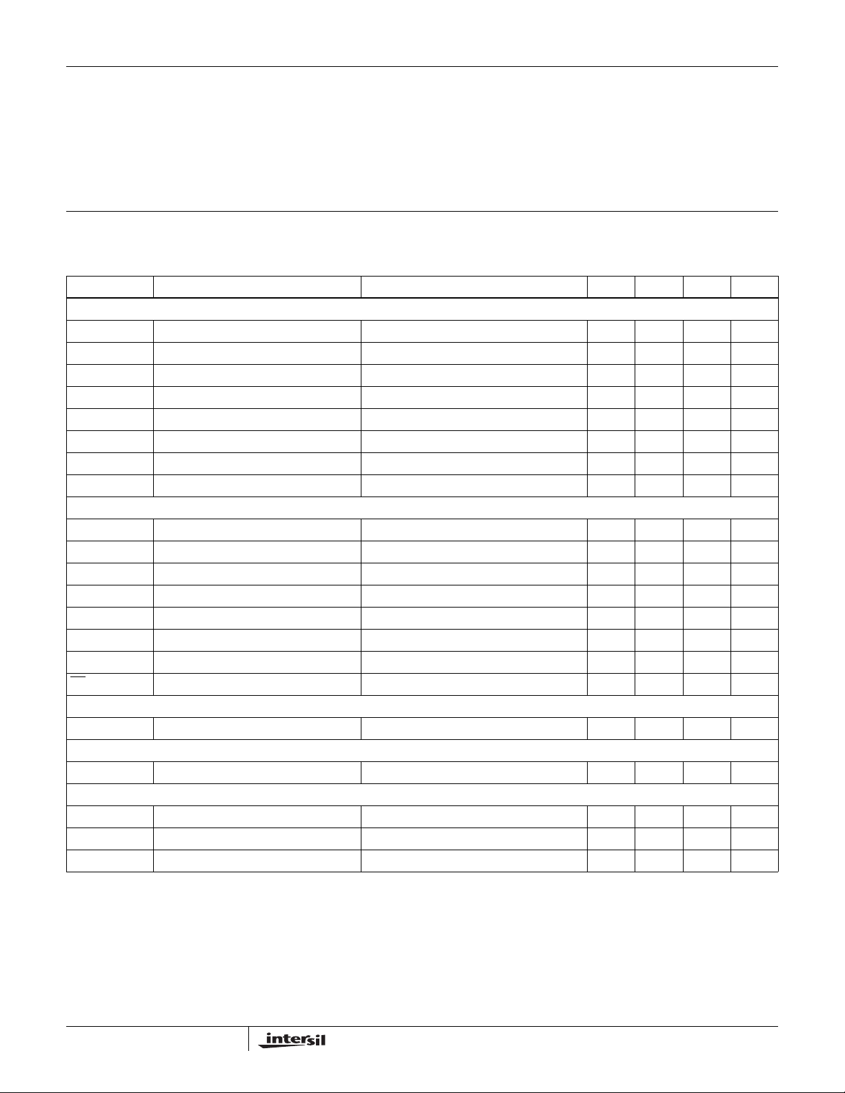
PARAMETER DESCRIPTION CONDITIONS MIN TYP MAX UNIT
AC PERFORMANCE
BW (-3dB) -3dB Bandwidth V
OUT
= 2V
P-P
350 MHz
SR Differential Slew Rate RL = 200Ω 600 1000 V/µs
T
STL
Settling Time to 0.1% 13.6 ns
GBW Gain Bandwidth Product 700 MHz
HD2 2nd Harmonic Distortion f = 20MHz, R
HD3 3rd Harmonic Distortion f = 20MHz, R
= 200Ω -70 dBc
L
= 200Ω -70 dBc
L
dP Differential Phase @ 3.58MHz 0.01 °
dG Differential Gain @ 3.58MHz 0.01 %
INPUT CHARACTERISTICS
V
OS
I
IN
Z
IN
V
DIFF
V
CM
V
N
CMRR Input Common Mode Rejection Ratio V
EN
Input Referred Offset Voltage -10 2 10 mV
Input Bias Current (VIN+, VIN+) -30 -15 -10 µA
Differential Input Impedance 180 kΩ
Differential Input Range ±0.75 V
Input Common Mode Voltage Range 0 2.3 V
Input Referred Voltage Noise 27 nV/√Hz
= 0 to 2V 60 80 dB
CM
Threshold 1.4 V
OUTPUT CHARACTERISTICS
I
OUT
Output Peak Current 40 60 mA
DC PERFORMANCE
A
V
Voltage Gain VIN = 0.8V
P-P
1.82 1.96 2.05 V/V
SUPPLY CHARACTERISTICS
V
SUPPLY
I
S
Supply Operating Range VS+ to VS-512V
Power Supply Current (per Channel) 12.3 14.5 16.2 mA
PSRR Power Supply Rejection Ratio 70 80 dB
3
FN7325.5
October 26, 2005
Page 4
EL4543
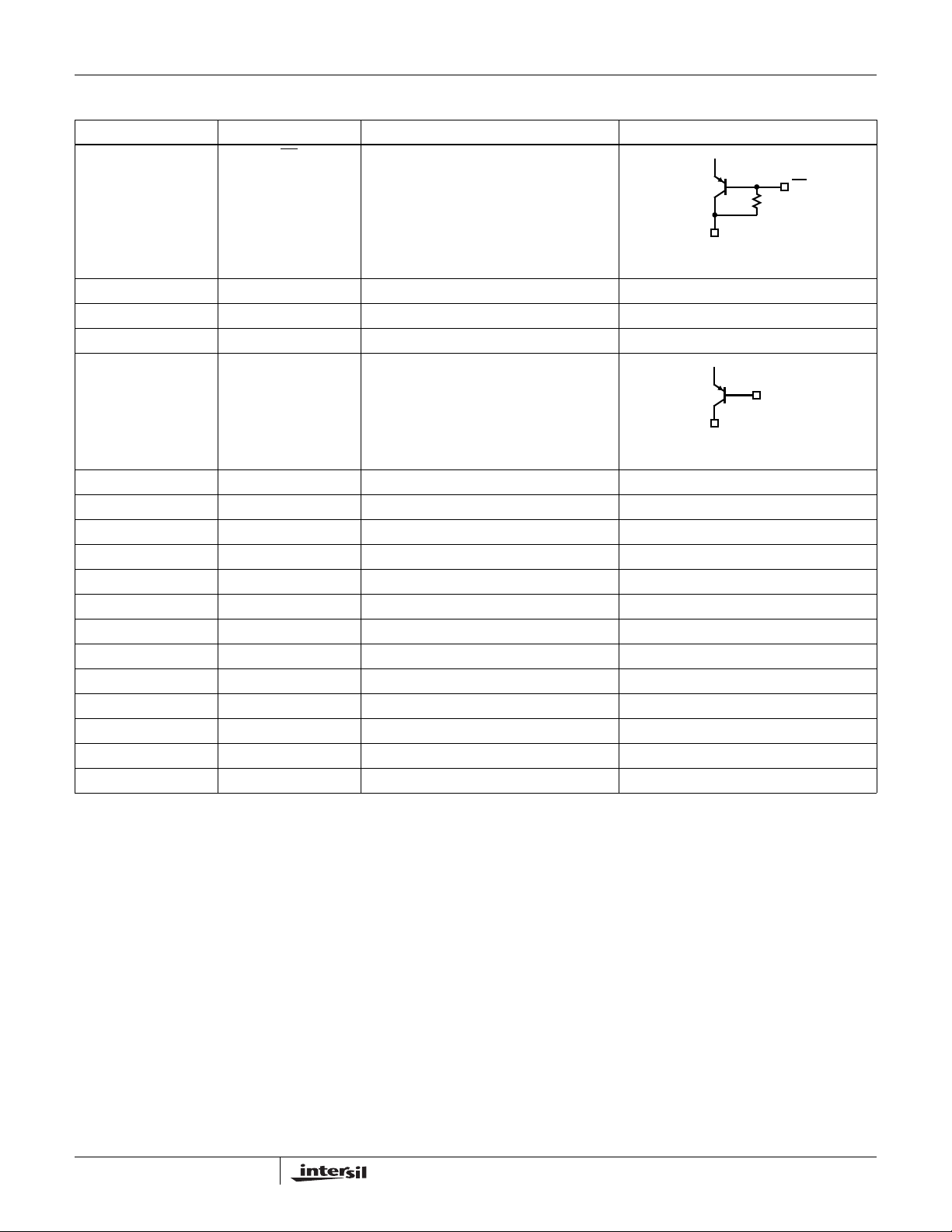
Pin Descriptions
PIN NUMBER PIN NAME PIN DESCRIPTION EQUIVALENT CIRCUIT
1EN
2 VINA+ Non-inventing input
3 VINA- Inverting input
4, 7, 10, 13, 16, 19, 22 NC Not connected
5 VSYNC Vertical sync logic input
6 HSYNC Horizontal sync logic input Reference Circuit 2
8 VINB+ Non-inverting input
9 VINB- Inverting input
11 VINC+ Non-inverting input
12 VINC- Inverting input
14 VOUTC- Inverting output
15 VOUTC+ Non-inverting output
17 VOUTB- Inverting output
18 VOUTB+ Non-inverting output
20 VS- Negative supply
21 VS+ Positive supply
23 VOUTA- Non-inverting output
24 VOUTA+ Inverting output
Disables video inputs and outputs
V
SM
CIRCUIT 1
V
SM
CIRCUIT 2
EN
SYNC
4
FN7325.5
October 26, 2005
Page 5
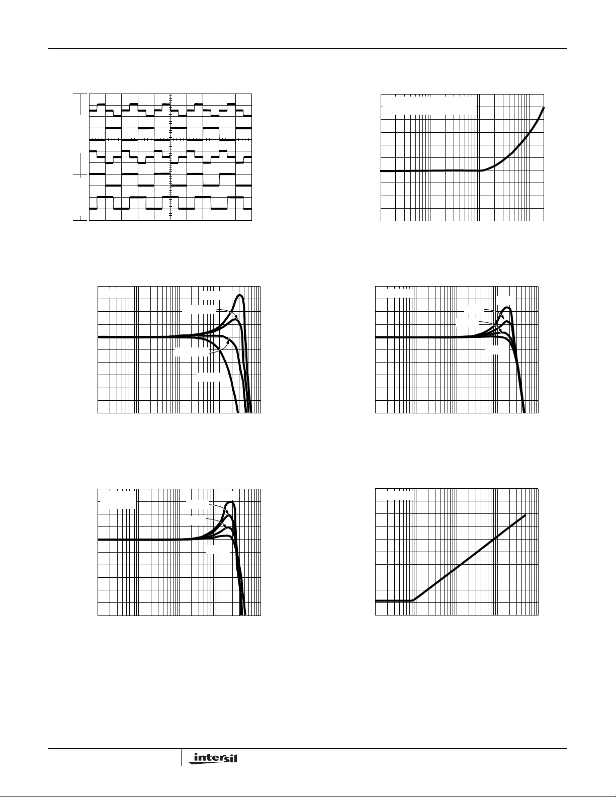
Typical Performance Curves
A
M
B
C
(0.5V/DIV)
VOLTAGE
(2.5V/DIV)
VOLTAGE
TIME (0.5ms/DIV)
FIGURE 1. COMMON MODE OUTPUT FIGURE 2. BALANCE ERROR
BLUE CM
OUT (CH
GREEN C
OUT (CH
RED CM
OUT (CH
V
SYNC
H
SYNC
EL4543
-42
BALANCE ERROR=
20 LOG(∆
-46
-50
-54
BALANCE ERROR (dB)
-58
-62
100K 1M 10M 100M
,CM/∆VO,DIFF)
VO
FREQUENCY (Hz)
4
CL=0pF
2
0
-2
-4
NORMALIZED GAIN (dB)
-6
100K 1M 10M
FREQUENCY RESPONSE (Hz)
RL=500Ω
RL=200Ω
RL=100Ω
RL=50Ω
100M 1G
FIGURE 3. DIFFERENTIAL FREQUENCY RESPONSE FOR
VARIOUS R
4
RL=100Ω
=2.2pF
C
L
2
0
-2
- DIFF
L
8.2pF
12pF
4.7pF
2.2pF
4
RL=200Ω
2
0
-2
-4
NORMALIZED GAIN (dB)
-6
100K 1M 10M
FREQUENCY RESPONSE (Hz)
12pF
8.2pF
22pF
2.2pF
100M 1G
FIGURE 4. DIFFFERENTIAL FREQUENCY RESPONSE FOR
VARIOUS CL - DIFF
0
RL=200Ω
20
40
60
-4
NORMALIZED GAIN (dB)
-6
100K 1M 10M
FREQUENCY RESPONSE (Hz)
FIGURE 5. DIFFERENTIAL FREQUENCY RESPONSE FOR
VARIOUS C
- DIFF
L
100M 1G
5
80
NORMALIZED GAIN (dB)
100
100K 1M 10M
FREQUENCY RESPONSE (Hz)
FIGURE 6. CMRR
100M 1G
October 26, 2005
FN7325.5
Page 6
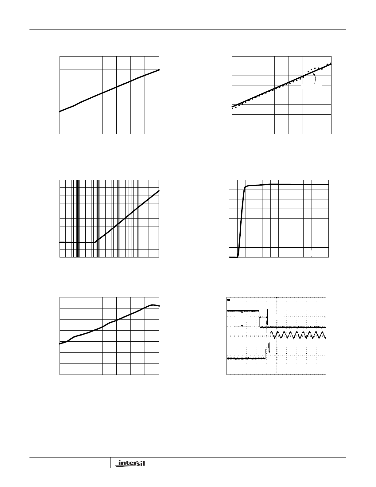
Typical Performance Curves (Continued)
T
EL4543
12
10
8
6
CMIR (V)
4
2
0
56 8
7911
SUPPLY VOLAGE (V)
10 12
FIGURE 7. COMMON MODE INPUT RANGE vs SUPPLY
VO LTAGE
0
-20
-40
-60
PSRR (dB)
-80
-100
0 10K 1M
FREQUENCY
10M 100M100K
FIGURE 9. PSRR vs FREQUENCY FIGURE 10. I
THRESHOLD (V)
RELATIVE TO NEGATIVE SUPPLY
FIGURE 8. H
0.04
0.035
0.03
0.025
0.02
0.015
CURRENT (A)
0.01
0.005
4
3.5
3
2.5
2
1.5
1
0.5
0
56 8
SUPPLY VOLAGE (V)
& V
SYNC
0
56 8
THRESHOLD vs SUPPLY VOLTAGE
SYNC
SUPPLY VOLAGE (V)
SUPPLY
V
SWITCH
10 127911
RL=200Ω
10 127911
vs V
SUPPLY
3.5
3
2.5
2
1.5
1
ENABLE DISABLE PIN (V)
0.5
0
56 8
2.5V
VOLTAGE (2V/DIV)
10 127911
SUPPLY VOLAGE (V)
212ns
TIME (200ns/DIV)
FIGURE 11. ENABLE DISABLE vs SUPPLY VOLTAGE FIGURE 12. ENABLE RESPONSE
6
ENABLE
OUTPU
SIGNAL
FN7325.5
October 26, 2005
Page 7
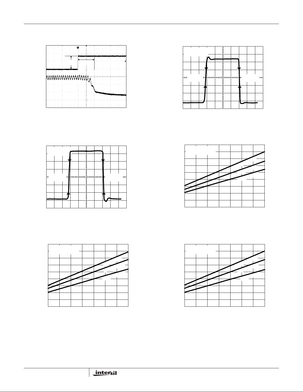
Typical Performance Curves (Continued)
T
2.5V
900ns
ENABLE
EL4543
RL=200Ω DIFF
C
=0pF
L
VOLTAGE (2V/DIV)
TIME (200ns/DIV)
OUTPU
SIGNAL
FIGURE 13. DISABLE RESPONSE FIGURE 14. DIFFERENTIAL SMALL SIGNAL TRANSIENT
RL=200Ω DIFF
=0pF
C
L
RISE
∆t=2.81ns
VOLTAGE (235mV/DIV)
TIME (20ns/DIV)
FALL
∆t=2.31ns
FIGURE 15. DIFFERENTIAL LARGE SIGNAL TRANSIENT
RESPONSE
RISE
∆t=25ns
VOLTAGE (120mV/DIV)
TIME (20ns/DIV)
FALL
∆t=1.94ns
RESPONSE
9
LOGIC H
8
V
SYNC
7
6
5
4
3
2
1
COMMON MODE DC LEVEL (V)
0
56 8
=0V
SYNC
=0V
SUPPLY VOLAGE (V)
N
E
E
R
G
B
-
M
C
D
E
R
A
-
M
C
UE
BL
C
-
CM
10 127911
FIGURE 16. COMMON MODE DC LEVEL vs SUPPLY
VOLTAGE
9
LOGIC H
V
SYNC
=3V
SYNC
8
7
6
5
4
3
2
1
COMMON MODE DC LEVEL (V)
0
56 8
=0V
SUPPLY VOLAGE (V)
D
E
R
A
-
M
C
C
M
C
10 127911
E
U
L
B
C
-
M
N
E
E
R
G
B
-
9
LOGIC H
V
SYNC
=0V
SYNC
8
7
6
5
4
3
2
1
COMMON MODE DC LEVEL (V)
0
56 8
=3V
C
SUPPLY VOLAGE (V)
N
E
E
R
G
B
-
M
C
10 127911
E
LU
B
C
-
M
D
E
R
A
-
M
C
FIGURE 17. COMMON MODE DC LEVEL vs SUPPLY VOLTAGE FIGURE 18. COMMON MODE DC LEVEL vs SUPPLY VOLTAGE
7
FN7325.5
October 26, 2005
Page 8
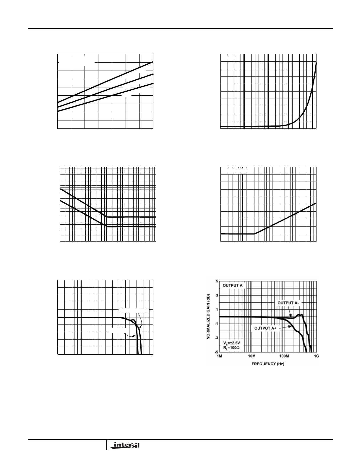
Typical Performance Curves (Continued)
EL4543
9
LOGIC H
V
SYNC
=3V
SYNC
8
7
6
5
4
3
2
1
COMMON MODE DC LEVEL (V)
0
56 8
=3V
SUPPLY VOLAGE (V)
E
U
L
B
C
-
M
C
C
10 127911
D
E
R
A
-
M
C
M
N
E
E
R
G
B
-
50
AV=+2
40
30
20
10
OUTPUT IMPEDANCE (Ω)
0
10K 100K 10M
FREQUENCY (Hz)
FIGURE 19. COMMON MODE DC LEVEL vs SUPPLY VOLTAGE FIGURE 20. OUTPUT IMPEDANCE
VOLTAGE NOISE (nV/√Hz),
10K
1K
100
10
CURRENT NOISE (pA/√Hz)
0
RL=200Ω DIFF
-20
-40
-60
CROSSTALK (dB)
-80
100M1M
1
56 8
FREQUENCY (Hz)
10 1279
-100
100K 1M 100M
10M
FREQUENCY (Hz)
FIGURE 21. INPUT VOLTAGE AND CURRENT NOISE FIGURE 22. CHANNEL ISOLATION vs FREQUENCY
5
3
1
-1
-3
NORMALIZED GAIN (dB)
-5
100K 1M 100M
10M
FREQUENCY (Hz)
FIGURE 23. FREQUENCY RESPONSE vs OUTPUT
V
OP-P
V
OP-P
=2V
=200mV
1G
FIGURE 24. GAIN vs FREQUENCY - 2 CHANNELS
AMPLITUDE
400M
8
FN7325.5
October 26, 2005
Page 9
EL4543
Typical Performance Curves (Continued)
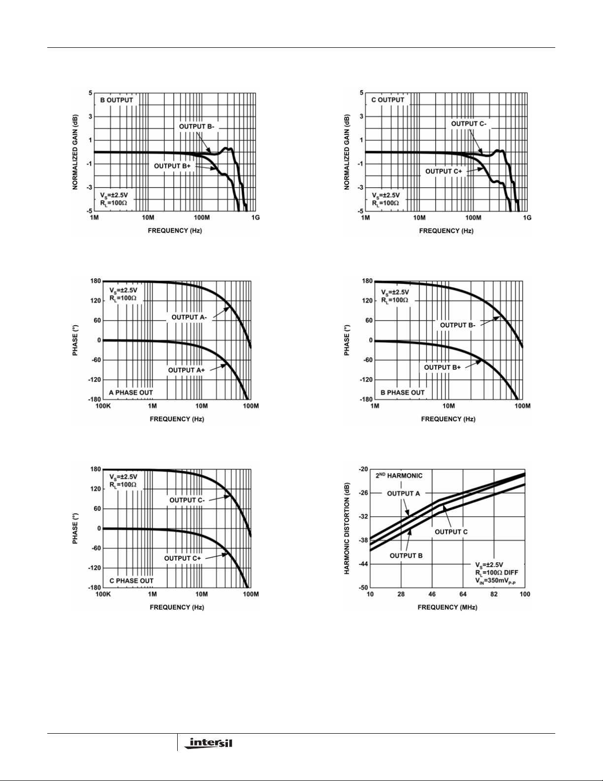
FIGURE 25. GAIN vs FREQUENCY - 2 CHANNELS FIGURE 26. GAIN vs FREQUENCY - 2 CHANNELS
FIGURE 27. PHASE vs FREQUENCY - 2 CHANNELS FIGURE 28. PHASE vs FREQUENCY - 2 CHANNELS
FIGURE 29. PHASE vs FREQUENCY - 2 CHANNELS FIGURE 30. HARMONIC DISTORTION
9
FN7325.5
October 26, 2005
Page 10
Typical Performance Curves (Continued)
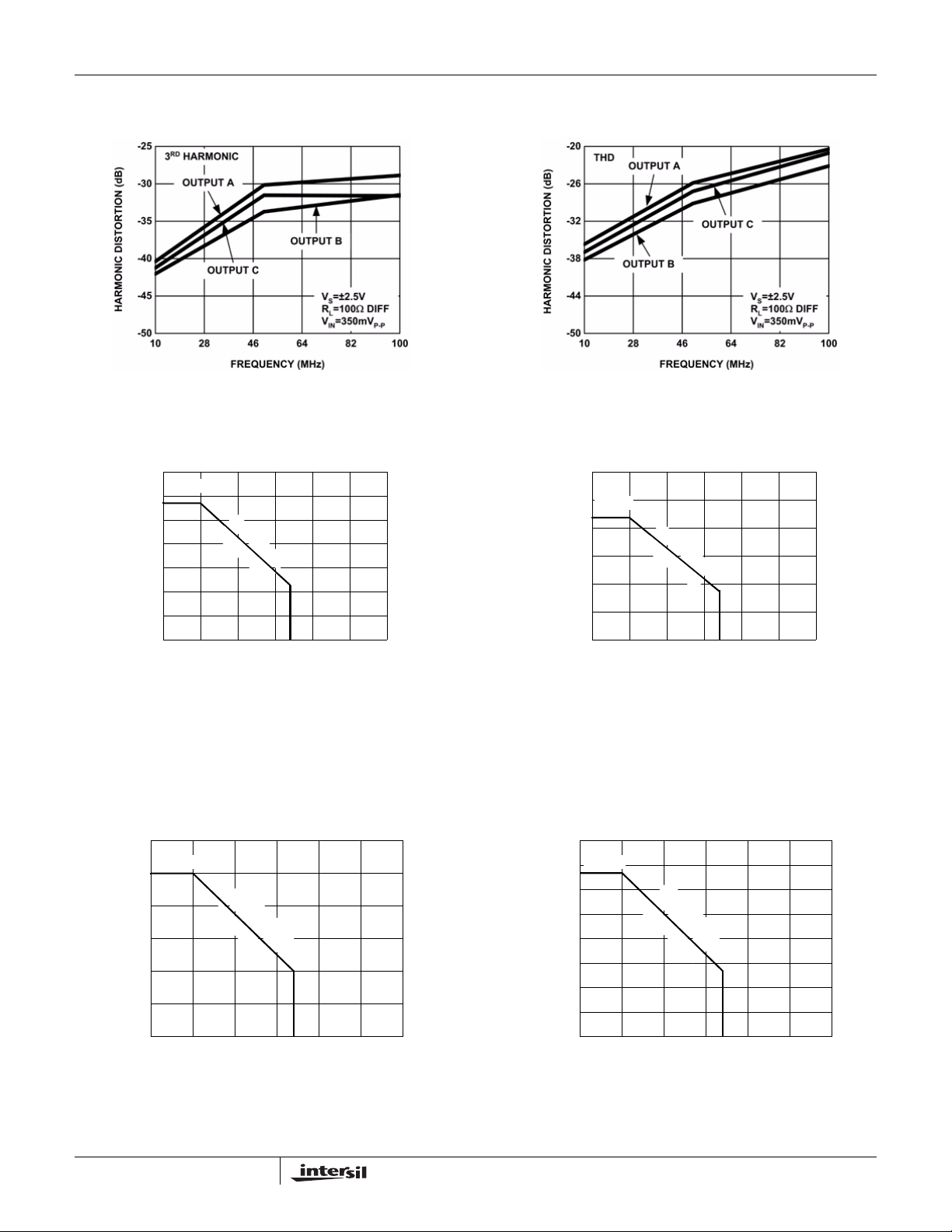
FIGURE 31. HARMONIC DISTORTION FIGURE 32. HARMONIC DISTORTION
EL4543
JEDEC JESD51-7 HIGH EFFECTIVE
THERMAL CONDUCTIVITY TEST BOARD
1.4
1.136W
1.2
1
0.8
0.6
0.4
0.2
POWER DISSIPATION (W)
0
0 255075100 150
Q
S
θ
O
J
A
P
=
2
8
4
8
°
C
/W
12585
AMBIENT TEMPERATURE (°C)
FIGURE 33. PACKAGE POWER DISSIPATION vs AMBIENT
TEMPERATURE
JEDEC JESD51-7 HIGH EFFECTIVE THERMAL
CONDUCTIVITY TEST BOARD - QFN EXPOSED
DIEPAD SOLDERED TO PCB PER JESD51-5
3
2.500W
2.5
(
4
Q
2
1.5
1
POWER DISSIPATION (W)
0.5
0
025 7510012585 15050
m
F
m
N
θ
2
JA
x
0
=
4
4
m
0
°
m
C
)
/
W
AMBIENT TEMPERATURE (°C)
FIGURE 35. PACKAGE POWER DISSIPATION vs AMBIENT
TEMPERATURE
JEDEC JESD51-3 LOW EFFECTIVE
THERMAL CONDUCTIVITY TEST BOARD
1.2
1
870mW
0.8
0.6
0.4
0.2
POWER DISSIPATION (W)
0
0 255075100 150
Q
S
θ
O
J
A
P
=
2
1
4
1
5
°
C
/
W
12585
AMBIENT TEMPERATURE (°C)
FIGURE 34. PACKAGE POWER DISSIPATION vs AMBIENT
TEMPERATURE
JEDEC JESD51-3 AND SEMI G42-88 (SINGLE
LAYER) TEST BOARD
0.8
667mW
0.7
0.6
0.5
0.4
0.3
0.2
POWER DISSIPATION (W)
0.1
0
025 7510012585 15050
(
4
Q
m
F
θ
m
N
J
2
A
x
0
=
4
1
m
5
0
m
°
C
)
/
W
AMBIENT TEMPERATURE (°C)
FIGURE 36. PACKAGE POWER DISSIPATION vs AMBIENT
TEMPERATURE
10
FN7325.5
October 26, 2005
Page 11
EL4543
Operational Description and Application
Information
Introduction
The EL4543 is designed to differentially drive composite
RGB video signals onto twisted pair lines, while
simultaneously encoding horizontal and vertical sync signals
as common mode output. The entire video signal plus sync
can therefore be transmitted on 3 twisted pairs of wire. When
utilizing CAT-5 cable, the 4th available twisted pair can be
used for transmission of audio, data or control information.
The distribution of composite video over standard CAT-5
cable enables enormous cost and labor savings compared
with traditional coaxial cable, when considering both the
relative low price and ease of pulling CAT-5 cable.
Functional Description
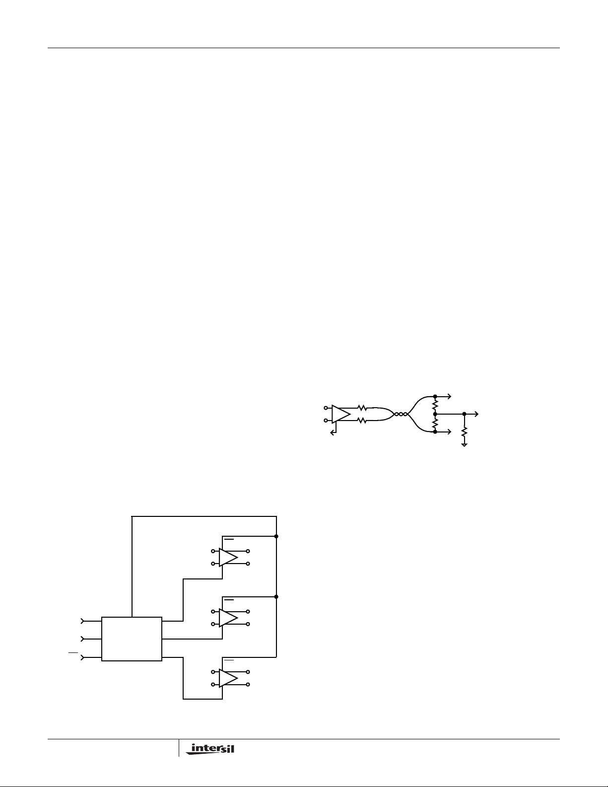
The EL4543 provides three fully differential high-speed
amplifiers, suitable for driving high-resolution composite
video signals onto twisted pair or standard coaxial cable.
The input common-mode range extends to the negative rail,
allowing simple ground-referenced input termination to be
used with a single supply. The amplifiers provide a fixed gain
of +2 to compensate for standard video cable termination
schemes. Horizontal and Vertical sync signals (H
V
) are passed to an internal Logic Encoding Block to
SYNC
encode the sync information as three discrete signals of
different voltage levels. Generally, in differential amplifiers an
external V
pin is used to control the common mode level
REF
of the differential output; in the case of the EL4543 the V
of each of the three internal amplifier channels receives a
signal from the Logic Encoding Block with encoded H
and V
information. The final output consists of three
SYNC
fully differential video signals, with sync encoded on the
common mode of each of the three RGB differential signals.
H
SYNC
and V
can easily be separated from the
SYNC
differential output signals, decoded and transmitted along
with the RGB video signals to the video monitor.
EN
+
+
INA OUTA
-
V
REF
V
H
SYNC
SYNC
EN
ENABLE/DISABLE
LOGIC
DECODING
FIGURE 37. BLOCK DIAGRAM EL4543
RCM
GCM
BCM
EN
+
+
INB OUTB
-
V
REF
EN
+
+
INC OUTC
-
V
REF
SYNC
+
-
+
-
+
-
and
REF
SYNC
Sync Transmission
The EL4543 encodes H
common mode output of the differential video signals; Red,
Green and Blue respectively. Data Sheet Figure 16, 17 and 18
clearly illustrate that the sum of the common mode voltages
results in a fixed average DC level with no AC content and
illustrates the logic levels. This eliminates EMI radiation into
any common mode signal along the twisted pairs of CAT 5
cable.
Extract Common Mode Sync and Decode H
V
SYNC
H
and V
SYNC
Mode sync output voltages. The relationships between
H
, V
SYNC
SYNC
Table 1. The common mode levels are easily separated from
the differential outputs of the EL4543 using this simple
resistor network at the cable receiver input of each
differential channel; see Figure 38.
can be regenerated from the Common
SYNC
and the 3 common mode levels are given by
SYNC
and V
signals on the
SYNC
SYNC
&
Twisted Pair Termination
The schematic in Figure 38 illustrates a termination scheme
for 50Ω series termination and a 100Ω twisted pair cable.
Note RCM is the common mode termination to allow
measurement of V
and should not be too small since it
CM
loads the EL4543; a little over a 100Ω is recommended for
RCM.
TYPICAL EL4543 TERMINATION DRIVER
TWISTED
V
50Ω
+
-
50Ω
REF
FIGURE 38. TWISTED PAIR TERMINATION EL4543
Z
PAI R
=100Ω
O
50Ω
50Ω
+
V
CM
120Ω
-
(RCM: SHOULD BE >100Ω)
(FOR LOADING
CONSIDERATIONS)
Video Transmission
The EL4543 is a twisted pair differential line driver directed
at the transmission of Video Signals through cables up to
100 feet; however, as signal losses increase with
transmission line length the EL4543 will need additional
support to equalize video signals along longer twisted pair
transmission lines. A full solution to accomplish this is the
SXGA Video Transmission System presented in the EL4543
Data Sheet. Note the inclusion of the EL9110 for signal
equalization of up to 1000ft of CAT-5 cable and common
mode extraction; see Data Sheet for additional information
on the EL9110.
Long Distance Video Transmission
The SXGA Video Transmission System makes it possible to
transmit Red, Green and Blue (RGB) video plus sync up to
1000 feet through CAT-5 cable. The input to the SXGA Video
Transmission System is the output of a video source
transmitting RGB video signals plus sync. The signals are
received initially by the EL4543; which converts the single
11
FN7325.5
October 26, 2005
Page 12

EL4543
ended input RGB signals to three fully differential waveforms
with sync encoded on the discrete common modes of each
color channel and then drives the signals through a length of
CAT-5 cable. The signal is received by the EL9110, which
can provide 6-pole equalization for both high and low
frequency signal transmission line losses. Then the EL9110
converts the differential RGB video signals back into single
ended format while extracting the common mode component
for decoding. The single ended RGB signal is taken directly
from the output of the El9110 and is ready for the output
device. The Common Mode Decoder Circuit receives the
common mode signals directly from each of the three
EL9110's common mode output pin, decodes and transmits
H
SYNC
and V
to the output device.
SYNC
Sync Transmission
The EL4543 encodes H
common mode output of the differential video signals; Red,
Green and Blue respectively. Data Sheet Figure 8 clearly
illustrates that the sum of the common mode voltages results
in a fixed DC level with no AC content; thus eliminating EMI
interference.
SYNC
and V
signals onto the
SYNC
Output Drive Protection
The EL4543 has internal short circuit protection set typically
at 60mA. if the output is shorted for extended periods of time
the increased power dissipation will eventually destroy the
part. To realize maximum reliability the output current should
never exceed 60mA. The 50Ω series back load matching
resistor provides additional protection.
Supply Voltage
While the EL4543 can be operated on ±5V split rails, single
supply 0V to 5V is the most common usage. It is very
important to note that the input logic thresholds are relative
to the negative supply pin, and therefore single supply,
ground referenced logic will not work when driving the
EL4543 on split rails. The amplifiers have an input common
mode range from 0V to 3.5V with a 0V to 5V supply. The
common mode output DC level range is a linear function of
the power supply, see Data Sheet Figures 15, 16, 17 &18.
The common mode input switching threshold as well as the
Enable/Disable input is a linear function of the supply
voltage, see Data Sheet Figure 1.
Disable and Power Down
The EL4543 provides an enable disable function which
powers down, logic input high, in 900ns and powers up, logic
input low, in 212ns. Disabled the amplifiers supply current is
reduced to 1.8mA (Positive Supply) and 0mA (Negative
Supply). Note that Enable/Disable threshold is a linear
function of the supply voltage levels. The Enable/Disable
threshold voltage level is compatible with standard
TTL/CMOS and referenced to the lowest supply potential.
Proper Layout Technique
A critical concern with any PCB layout is the establishment
of a “healthy” ground plane. It is imperative to provide
ground planes terminated close to inputs to minimize input
capacitance. Additionally, the ground plane can be
selectively removed from inputs to prevent load and supply
currents from flowing near the input nodes.
In general the following guidelines apply to all PCB layout:
• Keep all traces as short as possible.
• Keep power supply bypass components as close to the
chip as possible - extremely close.
• Create a healthy ground with low impedance and
continuous ground pathways available to all grounded
components board-wide.
• In high frequency applications on multi-level boards try to
keep one level of board with continuous ground plane and
minimum via cutouts - providing it is affordable.
• Provide extremely short loops from power pin to ground.
• If it is affordable, a ferrite bead is always of benefit to
isolate device from Power Supply noise and the rest of the
circuit from the noise of the device.
Power Dissipation Calculation
When switching at high speeds, or driving heavy loads, the
EL4543 drive capability is ultimately limited by the rise in die
temperature brought about by internal power dissipation. For
reliable operation die temperature must be kept below T
(125°C). It is necessary to calculate the power dissipation for
a given application prior to selecting package type. Power
dissipation may be calculated:
4
PD VSIS×()
× C
Σ
1
INTVS
2
f××()CLV
2
OUT
f××()+=
where:
•V
is the total power supply to the EL4543 (from VS+ to VS-)
S
•V
•C
•C
•I
is the swing on the output (VH - VL)
OUT
is the load capacitance
L
is the internal load capacitance (80pF max)
INT
is the quiescent supply current (40mA max)
S
• f is frequency
Having obtained the application's power dissipation, the
maximum junction temperature can be calculated:
T
JMAXTMAXΘJA
PD×+=
JMAX
12
FN7325.5
October 26, 2005
Page 13
T
EL4543
where:
•T
•T
is the maximum junction temperature (125°C)
JMAX
is the maximum ambient operating temperature
MAX
• PD is the power dissipation calculated above
• θJA is the thermal resistance, junction to ambient, of the
application (package + PCB combination). Refer to the
Package Power Dissipation curves.
Application Circuit
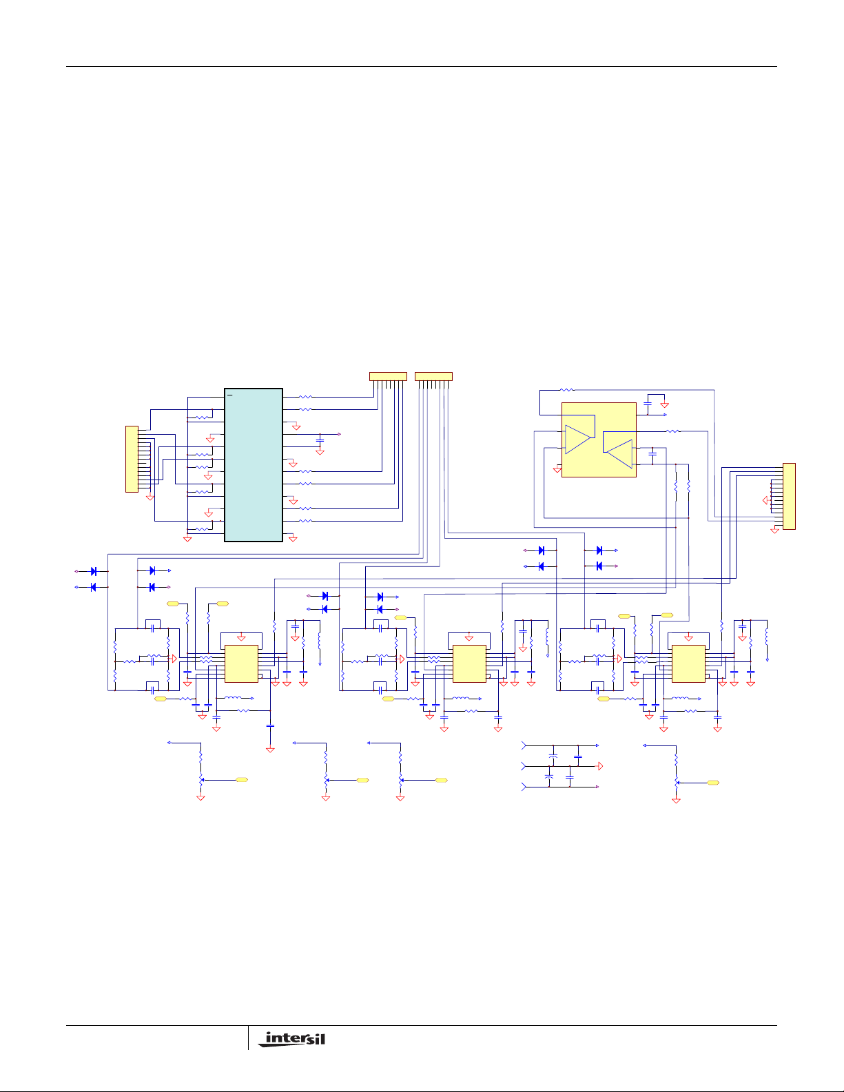
Video Transmission Along CAT-5 Cable
VGA input RGB plus sync is connected with 75Ω termination
to the inputs of the EL4543. Single-ended RGB video is
EL4543 & EL9110 Sync Extraction
8
RJOUTA+
OUTA+
OUTA-
OUTB+
OUTB-
OUTC+
49.9
24
23
RJOUTA-
49.9
22
N.C.
21
VS+
20
VS-
19
N.C.
RJOUTB+
49.9
18
17
RJOUTB-
49.9
16
N.C.
RJOUTC+
49.9
15
14
OUTC-
RJOUTC-
49.9
13
N.C.
INPUT
EL4543 QSOP
1
RED
1
GREEN
2
3
4
5
6
7
8
9
10
11
12
13
14
15
BLUE
RJA+ 75
RVSYNC 1K
RHSYNC
RJB+ 75
RJC+ 75
EN
2
INA+
3
INA-
4
N.C.
5
VSYNC
6
HSYNC
1K
7
N.C.
EL4543IU
8
INB+
9
INB-
10
N.C.
11
INC+
12
INC-
UJ1
NL
C1
R6 1K
C2 0.1uf
NL
C3
+VS
D2DIODE
-VS
D4DIODE
VCRTL
NL
R2
NL
R4
+VS
VadjBlu
R7
R8
330
3000
C6
1
2
3
4
5
6
7
0.1uf
Ctrl-ref
Vctrl
Vinp
Vinm
Vsm
Cmout
Vgain
Logic-ref8X2
EL9110 BLUE C
INDUCTOR 1
C7
R12
1uf
5
VadjBlue
EL9110
BLUE
Cmext
Vsp
Enbl
Vspo
Vout
Vsmo
0V
-VS
0.1uf
51
R10
51
C4
R11
1uf
R9
330
C5
1uf
R33
3.6K
R36
1K Pot
-VS
+VS
C9
1uf
75
R13
5
R14
16
15
14
13
12
11
C11
C10
0.1uf
10
9
C8
0.1uf
1K Pot
-VS
D1DIODE
+VS
D3
DIODE
Blue In Differential
R1
49.9
R5
49.9
R3
49.9
NL = Not Loaded
Inductor =Ferrite 68 Ohms
CAT1
Red Out Differential
+VS
0.1uf
C35
Green Out Diff erential
Blue Out Differential
D5
DIODE
DIODE
D7
Green InDifferential Red In Differential
INDUCTOR 2
+VS
R34
3.6K
R37 R38
D6DIODE
DIODE
NL
C12
R15
49.9
R30 1K
R29
49.9
C13 0.1uf
R17
49.9
NL
C14
+VS+VS
VGAN
converted to differential mode signals with H
V
encoded on the common-mode of the three
SYNC
SYNC
and
differential signals, respectively. The 50Ω output-terminated
EL4543 drives the differential RGB with sync encoded
common-mode to CAT-5 twisted pair cables. Note this
system, without signal frequency equalization, will
satisfactorily transmit along up to 200 feet of CAT-5 twistedpair. For longer cable lengths, frequency and gain
equalization to compensate for signal degradation is
recommended (EL9110) and a delay line technology
(EL9115) to adjust for phase mismatch between signals at
the receiving end.
1234567
1234567
+VS
-VS
D8
VCRTL
NL
R16
NL
R18
VGANVGAN
R35
3.6K
1K Pot
8
CAT2
R32 75
1
2
_
3
4
VS-
EL8201IS
-VS
DIODE
D9
+VS
D11DIODE
C20
1uf
330
R19
51
1
Ctrl-ref
R21
2
Vctrl
3
Vinp
4
Vinm
5
51
Vsm
6
R22
1uf
C17
0.1uf
7
EL9110 GREEN B
C18
1uf
VCRTL
Cmout
Vgain
Logic-ref8X2
R23
C15
R20
330
C16
1uf
R24
75
GREEN
16
Cmext
15
Vsp
14
Enbl
13
Vspo
12
EL9110
Vout
11
Vsmo
10
0V
9
5
C19
0.1uf
C21
0.1uf
GND
BANANA JACK
R25
C22
+VS
BANANA JACK
-VS
BANANA JACK
5
R26
49.9
INDUCTOR 4
+VS
0.1uf
R28
49.9
+
C36
4.7uf
+
C38
4.7uf
D10
DIODE
D12DIODE
NL
C23
R32 1K
R31
49.9
C24
0.1uf
NL
C25
VGAN
+VS
C37
0.1uF
C39
0.1uF
-VS
C34
0.1uf
8
VS+
+VS
R31 75
7
6
_
5
C35a
200pF
U3
+VS
-VS
VCRTL
R31
330
NL
51
R27
R32
51
C33
1uf
R33
NL
R29
R27
330
C27
0.1uf
C26
1uf
+VS
R30
R29
2K
2K
VadjRed
Rred4
3000
1
Ctrl-ref
Cmext
2
Vctrl
3
Vinp
4
Vinm
Vspo
5
Vsm
Vout
6
EL9110
Cmout
Vsmo
7
Vgain
Logic-ref8X2
EL9110 RED A
INDUCTOR 5INDUCTOR3
5
C28
R28
1uf
R39
3.6K
R40
1K Pot
RED
R25
C30
75
RED
16
15
Vsp
14
Enbl
13
12
0.1uf
11
C31
10
0V
9
-VS-VS
C29
0.1uf
VadjRed
GREEN
HSYNC
1
2
BLUE
3
4
5
6
7
8
9
10
11
12
13
VSYNC
14
15
OUTPU
1uf
5
INDUCTOR 6
R26
+VS
0.1uf
C32
13
FN7325.5
October 26, 2005
Page 14
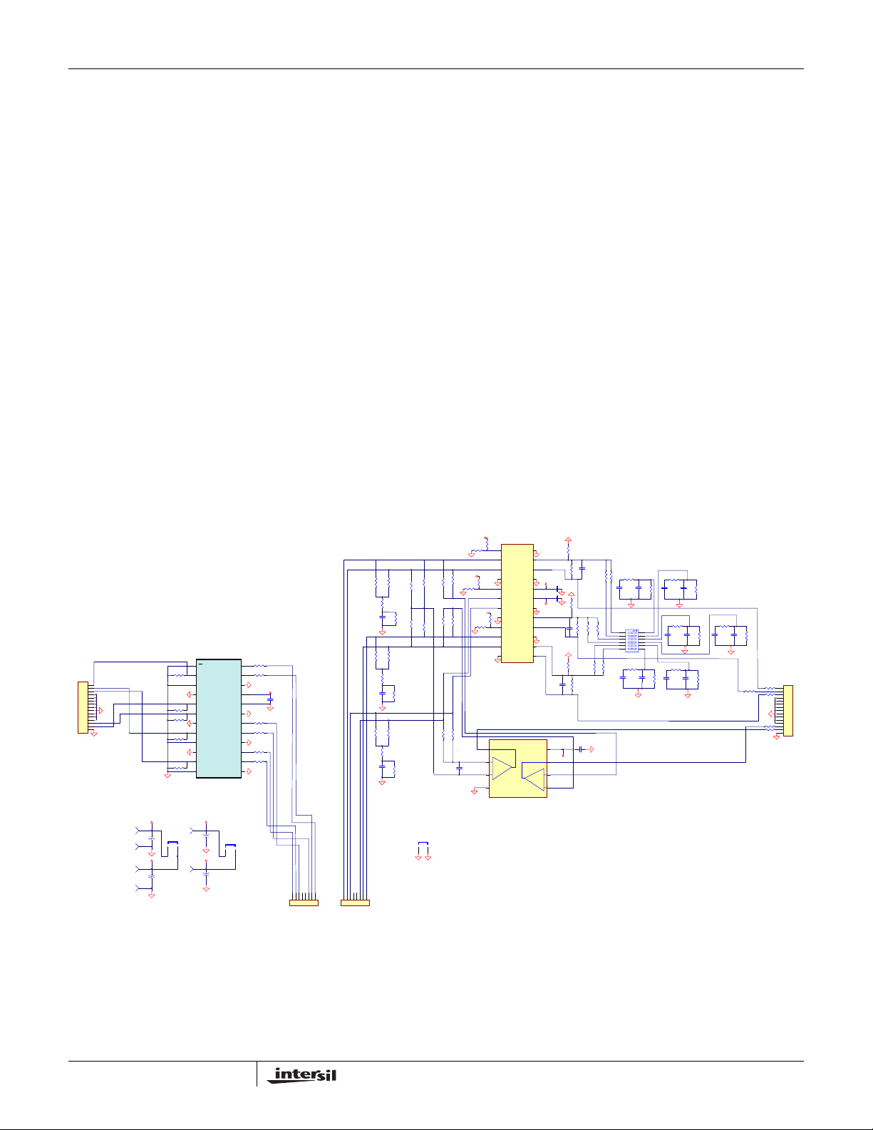
R1
75
R2
1K
R4
75
R5
75
R6
49.9
R7
49.9
Input +5V
EN
1
INA+
2
INA-
3
N.C.
4
HSYNC
6
N.C.
7
VSYNC
5
INB+
8
INB-
9
N.C.
10
INC+
11
INC-
12
N.C.
13
OUTC-
14
OUTC+
15
N.C.
16
OUTB-
17
OUTB+
18
N.C.
19
VS-
20
VS+
21
N.C.
22
OUTA-
23
OUTA+
24
EL4543 QSOP
EL4543IU
R8
49.9
R9
49.9
R10
49.9
R11
49.9
C1
0.1uf
R3 1K
Red In
Green In
Blue In
Red Out Differential
Green Out Differential
Blue Out Differential
1234567
8
OUTPUT
REF1
1
INP1
2
INN1
3
NC
4
REF2
5
INP2
6
INN2
7
NC
8
REF3
9
INP3
10
INN3
11
NC12OUT3
13
FB3
14
EN
15
OUT2
16
FB2
17
NC
18
VSN
19
VSP
20
NC
21
OUT1
22
FB1
23
NC
24
U2
EL5375
R28
499
R28
499
R31
499
R30
499
R32
499
R33
499
R25
2K
R27
2K
R24
2K
R26
2K
1
2
3
4
5
6
7
8
9
10
11
12
13
14
15
OUTPUT
1234567
8
INPUT
R12
57
R13
57
R14
49.9
R16
57
R17
49.9
R1855R19
55
R20
49.9
C6
0.1uF
Output +5V
Output -5V
1
2
3
4
5
6
7
8
9
10
11
12
13
14
15
INPUT
R36
Open
R37
0
Output +5V
R41
2K
R40
2K
R54
68K
R47
500
R53 10K
R48
1K
C7
36p
C8
10p
R56
33K
R55 3.9K
C9
68p
C10
22p
150 Feet Comp
300 Feet Comp
R44
2K
R43
2K
R46
2K
R45
2K
R63
75
R65 75
R64
75
R66 75
R67 75
R64
68K
R51
1K
R63 10K
R52
500
C17
36p
C18
10p
R62
33K
R61
3.9K
C15
68p
C16
22p
150 Feet Comp
300 Feet Comp
JB1
+VS In
JB3
GND
JB2
-VS In
Input -5VInput +5V
JB4
+VS Out
JB6
GND
JB5
-VS Out
Output -5VOutput +5V
1
2
JP+
JUMPER
1
2
JP-
JUMPER
+
Csup1
4.7uF
+
Csup2
4.7uF
+
Csup3
4.7uF
+
Csup4
4.7uF
R15
57
R58
68K
R49
500
R57 10K
R50
1K
C11
36p
C12
10p
R60
33K
R59 3.9K
C13
68p
C14
22p
150 Feet Comp 300 Feet Comp
R34
Open
R35
0
Output +5V
R38
Open
R39
0
Output +5V
1
2
3
4
5
6
12
11
10
9
8
7
Compensation Control Switch
SW DIP-6
1
2
3
VS-
4
5
6
7
VS+
8
_
_
U3
EL8201IS
Output +5V
C19
0.1uF
C3
0.1uF
C2
0.1uF
C4
0.1uF
C5
0.1uF
1
2
Ground
JUMPER
R22
1K
R21
1K
R23
1K
On Off
C20
~4pF
C21
~4pF
C22
~4pF
C4a
220pF
EL4543
EL4543/EL5375/EL8201 CAT-5 RGB +
Sync Video Transmission System
Introducing a low cost turn-key system for transmitting
component video over short to moderate CAT-5 cable
lengths (1 to 500 feet) with selectable cable loss and skew
compensation. Using only 3 of the 4 pairs in standard CAT-5
th
the 4
pair is available for audio, function control or data
transmission; an additional benefit.
RGB video plus sync (5 channels) is received at the VGA
terminal and presented single ended to the EL4543. The
EL4543 converts single ended RGB into fully differential
signals on three twisted pairs. Sync is encoded on the three
RGB differential signals as differential common mode and
then drives the differential signals with encoded sync
through CAT-5 cable. The common mode of the signals is
extracted from the differential signals with a passive network
of resistors and passed to the EL8201 for sync decoding.
The differential signal is passed directly to the EL5375 where
it is amplified, converted back into single ended format.
Signal attenuation occurs in all transmission lines as a
function of increasing cable length; this application system
utilizes individual channel 2-pole compensation for cable
lengths of 150, 300 and 500 feet. Additionally, the
compensation network can be manipulated to provide some
measure of cable prop delay skew compensation for slight
differences in cable lengths between CAT-5 pairs. Cable
skew can best be done around the 300 ft range by under
compensating the shortest color pair (color on the left side of
a vertical line) and over compensate the longest color pair
(color on the right side of a vertical line). Around 450 ft only
the shortest color pair can be under compensated.
The board for the driver and receiver should use strip lines
or strip line waveguides for the inputs and outputs of the
drivers and receivers. The 75Ω input and output strip lines
waveguide on 0.06 inch epoxy board with ground back plain
should be 0.016 inch wide with 0.01 inch space to ground
area around them. The diff pair strip line waveguides should
be two 0.045 inch 50Ω lines spaced 0.01 inch apart and
spaced 0.01 inch to ground area around them. This is a
general guide and size values may very for many reasons.
The receiver feedback and gain resistor network which goes
directly to the minus input should be connected very close
with minimal trace length and minimal capacitance to
ground. The ground plane on the backside of the board, in
back of these resistors and the minus input pin should be
removed as well.
14
FN7325.5
October 26, 2005
Page 15
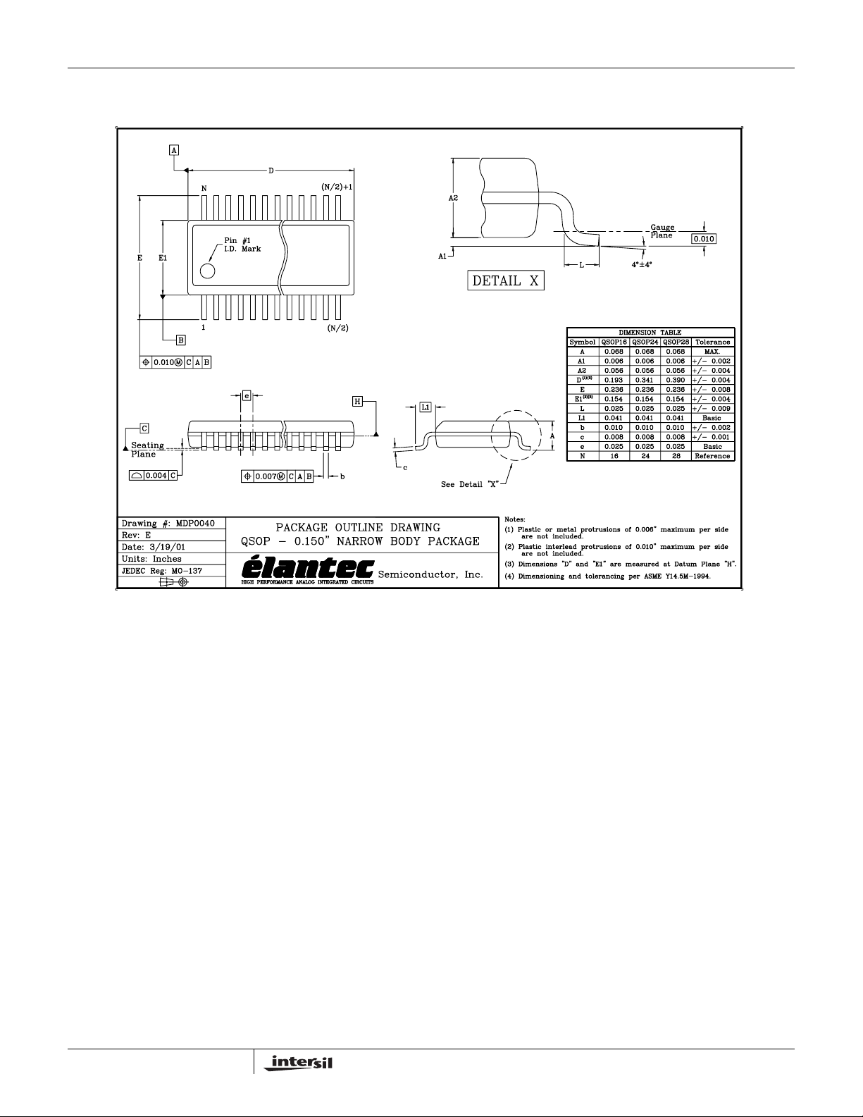
QSOP Package Outline Drawing
EL4543
15
FN7325.5
October 26, 2005
Page 16
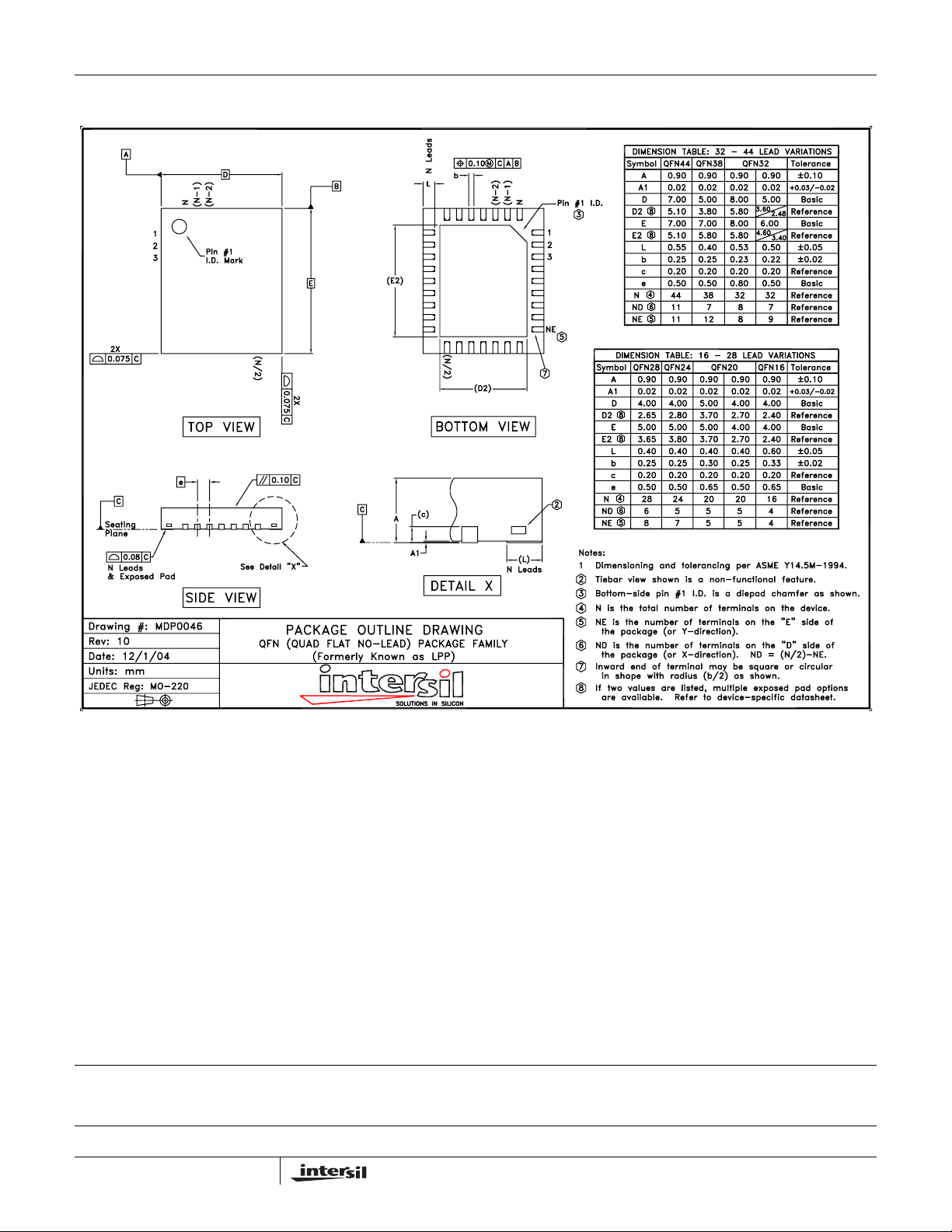
QFN Package Outline Drawing
EL4543
NOTE: The package drawings shown here may not be the latest version. To check the latest revision, please refer to the Intersil website at
http://www.intersil.com/design/packages/index.asp
All Intersil U.S. products are manufactured, assembled and tested utilizing ISO9000 quality systems.
Intersil Corporation’s quality certifications can be viewed at www.intersil.com/design/quality
Intersil products are sold by description only. Intersil Corporation reserves the right to make changes in circuit design, software and/or specifications at any time without
notice. Accordingly, the reader is cautioned to verify that data sheets are current before placing orders. Information furnished by Intersil is believed to be accurate and
reliable. However, no responsibility is assumed by Intersil or its subsidiaries for its use; nor for any infringements of patents or other rights of third parties which may result
from its use. No license is granted by implication or otherwise under any patent or patent rights of Intersil or its subsidiaries.
For information regarding Intersil Corporation and its products, see www.intersil.com
16
FN7325.5
October 26, 2005
 Loading...