

Page 1
®
EL4581
Data Sheet August 16, 2002
Sync Separator , 50% Slice, S-H, Filter
The EL4581 extracts timing information from standard negative going
video sync found in NTSC, PAL, and
SECAM broadcast systems. It can also be used in non standard formats and with computer graphics systems at higher
scan rates, by adjusting a single external resistor. When the
input does not have correct serration pulses in the vertical
interval, a default vertical output is produced.
Outputs are composite sync, vertical sync, burst/back porch
output, and odd/even output. The later operates only in interlaced scan formats.
The EL4581 provides a reliable method of determining correct sync slide level by setting it to the mid-point between
sync tip and blanking level at the back porch. This 50% level
is determined by two internal self timing sample and hold circuits that track sync tip and back porch levels. This also
provides a degree of hum and noise rejection to the input signal, and compensates for varying input levels of 0.5
2.0V
P-P
.
A built in linear phase, third order, low pass filter attenuates
the chroma signal in color systems to prevent incorrectly set
color burst from disturbing the 50% sync slide.
This device may be used to replace the industry standard
LM1881, offering improved performance and reduced power
consumption.
P-P
to
FN7172
Features
• NTSC, PAL and SECAM sync separation
• Single supply, +5V
• Precision 50% slicing, internal caps
• Built-in color burst filter
• Decodes non-standard verticals
• Pin compatible with LM1881
•Low power
• Typically 1.5mA supply current
• Resistor programmable scan rate
• Few external components
• Available in 8-pin PDIP and SO packages
Applications
• Video special effects
• Video test equipment
• Video distribution
• Displays
•Imaging
• Video data capture
• Video triggers
The EL4581 video sync separator is manufactured using
Elantec’s high performance analog CMOS process.
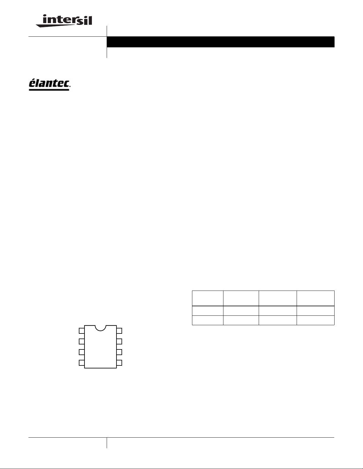
Pinout
EL4581
(8-Pin SO, DIP)
TOP VIEW
COMPOSITE
SYNC OUT
COMPOSITE
VIDEO IN
VERTICAL
SYNC OUT
All other trademarks mentioned are the property of their respective owners. Manufactured under U.S. Patent 5,528,303. Manufactured under License, U .S . Patents 5,486,869; 5,754,250.
GND
1
2
3
4
1
8
VDD 5V
7
ODD/EVEN OUTPUT
RSET
6
BURST/BACK
5
PORCH OUTPUT
CAUTION: These devices are sensitiv e to electrostatic discharge; follow proper IC Handling Procedures.
Copyright © Intersil Americas Inc. 2003. All Rights Reserved. Elantec is a registered trademark of Elantec Semiconductor, Inc.
1-888-INTERSIL or 321-724-7143
Ordering Information
PART
NUMBER
EL4581CN -40°C to +85°C 8-Pin PDIP MDP0031
EL4581CS -40°C to +85°C 8-Pin SO MDP0027
TEMP.
RANGE PACKAGE PKG. NO.
Demo Board
A dedicated demo board is not available. However, this
device can be placed on the EL4584/5 Demo Board.
| Intersil (and design) is a registered trademark of Intersil Americas Inc.
Page 2
EL4581
Absolute Maximum Ratings (T
Supply . . . . . . . . . . . . . . . . . . . . . . . . . . . . . . . . . . . . . . . . . .7V
V
CC
Storage Temperature. . . . . . . . . . . . . . . . . . . . . . . .-65°C to +150°C
Pin Voltages. . . . . . . . . . . . . . . . . . . . . . . . . . . . -0.5V to V
CAUTION: Stresses above those listed in “Absolute Maximum Ratings” may cause permanent damage to the device. This is a stress only rating and operation of the
device at these or any other conditions above those indicated in the operational sections of this specification is not implied.
IMPORTANT NOTE: All parameters having Min/Max specifications are guaranteed. Typical values are for information purposes only. Unless otherwise noted, all tests
are at the specified temperature and are pulsed tests , therefore: T
DC Electrical Specifications Unless otherwise state V
= 25 °C)
A
+0.5V
CC
= TC = T
J
Operating Temperature Range . . . . . . . . . . . . . . . . .-40°C to +85°C
Junction Temperature . . . . . . . . . . . . . . . . . . . . . . . . . . . . . . . 150°C
Power Dissipation . . . . . . . . . . . . . . . . . . . . . . . . . . . . . See Curves
A
= 5V, TA = 25°C, R
DD
SET
= 680kΩ.
PARAMETER DESCRIPTION TEMP MIN TYP MAX UNIT
I
DD
VDD = 5V (Note 1) 25°C 0.75 1.7 3 mA
Clamp Voltage Pin 2, Unloaded 25°C 1.3 1.5 1.9 V
Discharge Current Pin 2 = 2V 25°C 6 10 20 µA
Clamp Charge Current Pin 2, V
Ref Voltage Pin 6, V
= 1V 25°C 2 3 mA
IN
= 5V (Note 2) 25°C 1.5 1.8 2.1 V
DD
VOL Output Low Voltage IOL = 1.6mA 25°C 800 mV
V
Output High Voltage IOH = -40µA 25°C 4 V
OH
I
= -1.6mA 25°C 2.4 V
OH
NOTES:
1. No video signal, outputs unloaded.
2. Tested for V
5V ±5% which guarantees timing of output pulses over this range.
DD
Dynamic Specifications V
= 5V, IVpk-pk video, TA = 25°C, CL = 15pF, IOH = -1.6mA, IOL = 1.6mA. Signal voltages are peak to peak.
DD
PARAMETER DESCRIPTION TEMP MIN TYP MAX UNIT
Vertical Sync Width, t
Burst/Back Porch Width, t
VS
B
Vertical Sync Default Delay t
Filter Attenuation F
Composite Sync Prop Delay V
(Note 1) 25°C 190 230 300 µs
(Note 1) 25°C 2.5 3.5 4.5 µs
VSD
= 3.4MHz (Note 2) 25°C 24 dB
IN
- Composite Sync (Note 1) 25°C 260 400 ns
IN
25°C405570µs
Input Dynamic Range p-p NTSC Signal (Note 3) 25°C 0.5 2 V
Slice Level Input Voltage = 1V
P-P
25°C 40% 50% 60%
(Note 4) Full 40% 50% 60%
NOTES:
1. C/S, Vertical and Burst outputs are all active low - V
2. Attenuation is a function of R
3. Typical min. is 0.3V
4. Refers to threshold level of sync. tip to back porch amplitude.
P-P
.
SET
(PIN6).
= 2.4V, VOL = 0.8V.
OH
2
Page 3

EL4581
Pin Descriptions
PIN NUMBER PIN NAME FUNCTION
1 Composite Sync Out Composite sync pulse output. Sync pulses start on a falling edge and end on a rising edge.
2 Composite Video in AC coupled composite video input. Sync tip must be at the lowest potential (Positive picture phase).
3 Vertical Sync Out Vertical sync pulse output. The falling edge of Vert Sync is the start of the vertical period.
4 GND Supply ground.
5 Burst/Back Porch Output Burst/Back porch output. Low during burst portion of composite video.
6R
7 Odd/Even Output Odd/Even field output. Low during odd fields, high during even fields. Transitions occur at start of
8V
NOTE 1. R
SET
(Note 1) An external resistor to ground sets all internal timing. 681k, 1% resistor will provide correct timing
SET
5V Positive supply. (5V)
DD
must be a 1% resistor.
for NTSC signals.
Vert Sync pulse.
3
Page 4

Typical Performance Curves
R
vs Horizontal
SET
Frequency
EL4581
Back Porch Clamp
On Time vs R
SET
Vertical Pulse Width
vs R
SET
Vertical Default Delay
Time vs R
SET
Package Power Dissipation vs Ambient Temperature
JEDEC JESD51-3 Low Effective Thermal Conductivity Test Board
1.8
1.6
1.4
1.25W
1.2
1
781mW
0.8
0.6
0.4
Power Dissipation (W)
θ
0.2
0
0 25 50 75 100 125 150
PDIP8
θ
=100°C/W
JA
SO8
=160°C/W
JA
Ambient Temperature (°C)
85
Vertical Pulse Width
vs Temperature
Input Signal = 300mV
EL4581 Filter Characteristic
Constant Delay 240ns
P-P
Package Power Dissipation vs Ambient Temperature
JEDEC JESD51-7 High Effective Thermal Conductivity Test Board
2
1.8
1.6
1.4
1.2
1
0.8
0.6
Power Dissipation (W)
0.4
0.2
0
0 25 50 75 100 125 150
1.471W
1.136
PDIP8
θ
=85°C/W
JA
SO8
θ
=110°C/W
JA
Ambient Temperature (°C)
Supply Current
vs Temperature
85
4
Page 5

Timing Diagrams
EL4581
NOTES:
b. The composite sync output reproduces all the video input sync pulses, with a propagation delay.
c. Vertical sync leading edge is coincident with the first vertical serration pulse leading edge, with a propagation delay.
d. Odd-even output is low for even field, and high for odd field.
e. Back porch goes low for a fixed pulse width on the trailing edge of video input sync pulses. Note that for serration pulses during vertical, the back porch starts
on the rising edge of the serration pulse (with propagation delay).
FIGURE 1.
5
Page 6

Timing Diagrams (Continued)
EL4581
FIGURE 2.
6
Page 7

Timing Diagrams (Continued)
EL4581
FIGURE 3.
FIGURE 4. STANDARD (NTSC INPUT) H. SYNC DETAIL
7
Page 8

EL4581
Description of Operation
A simplified block schematic is shown in Figure 2. The following description is intended to provide the user with sufficient
information to be able to understand the effects that the
external components and signal conditions have on the outputs of the integrated circuit.
The video signal is AC coupled to pin 2 via the capacitor C
nominally 0.1µF. The clamp circuit A1 will prevent the input
signal on pin 2 going any more negative than 1.5V, the value
of reference voltage V
. Thus the sync tip, the most nega-
R1
tive part of the video waveform, will be clamped at 1.5V. The
current source I
, nominally 10µA, charges the coupling
1
capacitor during the remaining portion of the H line, approximately 58µs for a 15.75kHz timebase. From I • t = C • V, the
video time-constant can be calculated. It is important to note
that the charge taken from the capacitor during video must
be replaced during the sync tip time, which is much shorter,
(ratio of x 12.5). The corresponding current to restore the
charge during sync will therefore be an order of magnitude
higher, and any resistance in series with C
will cause sync
I
tip crushing. For this reason, the internal series resistance
has been minimized and external high resistance values in
series with the input coupling capacitor should be avoided.
The user can exercise some control over the value of the
input time constant by introducing an external pull-up resistance from pin 2 to the 5V supply. The maximum voltage
across the resistance will be V
less 1.5V, for black level.
DD
For a net discharge current greater than zero, the resistance
should be greater than 450k. This will have the effect of
increasing the time constant and reducing the degree of picture tilt. The current source I
current I
and thus increases with scan rate adjustment, as
TR
directly tracks reference
1
explained later.
The signal is processed through an active 3 pole filter (F1)
designed for minimum ripple with constant phase delay. The
filter attenuates the color burst by 24dB and eliminates fast
transient spikes without sync crushing. An external filter is
not necessary. The filter also amplifies the video signal by
6dB to improve the detection accuracy. Note that the filter
cut-off frequency is a function of R
proportional to I
OT
.
Internal reference voltages (block V
through IOT and is
SET
) with high immunity
REF
to supply voltage variation are derived o n the chip. Reference V
with op-amp A2 forces pin 6 to a reference voltage
R4
of 1.7V nominal. Consequently, it can be seen that the external resistance R
current I
. The internal resistance R3 is only about 6kΩ,
TR
much less than R
chip are referenced to I
will determine the value of the reference
SET
. All the internal timing functions on the
SET
and have excellent supply voltage
TR
rejection.
1
fixed level above the clamp voltage V
. The output of C2
R1
initiates the timing one-shots for gating the sample and hold
circuits. The sample of the sync tip is delayed by 0.8µs to
enable the actual sample of 2µs to be taken on the optimum
section of the sync. pulse tip. The acquisition time of the circuit is about three horizontal lines. The double poly CMOS
technology enables long time constants to be achieved with
,
small high quality on-chip capacitors. The back porch voltage
is similarly derived from the trailing edge of sync, which also
serves to cut off the tip sample if the gate time exceeds the
tip period. Note that the sample and hold gating times will
track RSET through I
OT
.
The 50% level of the sync tip is derived, through the resistor
divider R1 and R2, from the sample and held voltages V
and V
, and applied to the plus input of comparator C1.
BP
TIP
This comparator has built in hysteresis to avoid false triggering. The output of C2 is a digital 5V signal which feeds the
C/S output buffer B1 and the other internal circuit blocks, the
vertical, back porch and odd/even functions.
The vertical circuit senses the C/S edges and initiates an
integrator which is reset by the shorter horizontal sync pulses
but times out the longer vertical sync. pulse widths. The
internal timing circuits are referenced to I
and VR3, the
OT
time-out period being inversely proportional to the timing current. The vertical output pulse is started on the first serration
pulse in the vertical interval and is then self-timed out. In the
absence of a serration pulse, an internal timer will default the
start of vertical.
The back porch is triggered from the sync tip trailing edge
and initiates a one-shot pulse. The period of this pulse is
again a function of I
set by R
SET
.
and will therefore track the scan rate
OT
The odd/even circuit (O/E) comprises of flip flops which track
the relationship of the horizontal pulses to the leading edge
of the vertical output, and will switch on every field at the start
of vertical. Pin 7 is high during the odd field.
Loss of video signal can be detected by monitoring the C/S
output. The 50% level of the previous video signal will remain
held on the S/H capacitors after the input video signal has
gone and the input on pin 2 has defaulted to the clamp voltage. Consequently the C/S output will remain low longer than
the normal vertical pulse period. An external timing circuit
could be used to detect this condition.
Comparator C2 on the input to the sample and hold block
(S/H) compares the leading and trailing edges of the sync.
pulse with a threshold voltage V
which is referenced at a
R2
8
Page 9

Block Diagram
EL4581
*Note:
RSET must be
a 1% resistor.
FIGURE 5. STANDARD (NTSC INPUT) H. SYNC DETAIL
All Intersil U.S. products are manufactured, assembled and tested utilizing ISO9000 quality systems.
Intersil Corporation’s quality certifications can be viewed at www.intersil.com/design/quality
Intersil products are sold by description only. Intersil Corporation reserves the right to make changes in circuit design, software and/or specifications at any time without
notice. Accordingly, the reader is cautioned to verify that data sheets are current before placing orders. Information furnished by Intersil is believed to be accurate and
reliable. However, no responsibility is assumed by Intersil or its subsidiaries for its use; nor for any infringements of patents or other rights of third parties which may result
from its use. No license is granted by implication or otherwise under any patent or pat ent rights of In tersi l or its subs idiaries.
For information regarding Intersil Corporation and its products, see www.intersil.com
9
 Loading...