

查询EL4332CS-T13供应商
®
EL4332
Data Sheet October 4, 2004
Triple 2:1 300MHz Mux-Amp AV = 2
The EL4332 is a triple very high speed 2:1 MultiplexerAmplifier. It is intended primarily for component video
multiplexing and is especially suited for pixel switching. The
amplifiers have their gain set to 2 internally, which reduces
the need for many external components. The gain-of-2
facilitates driving back terminated cables. All three amplifiers
are switched simultaneously from their A to B inputs by the
TTL/CMOS compatible, common A/B control pin.
A -3dB bandwidth of 300MHz together with 3ns multiplexing
time enable the full performance of the fastest component
video systems to be realized.
The EL4332 runs from standard ±5V supplies, and is
available in the narrow 16-pin small outline package.
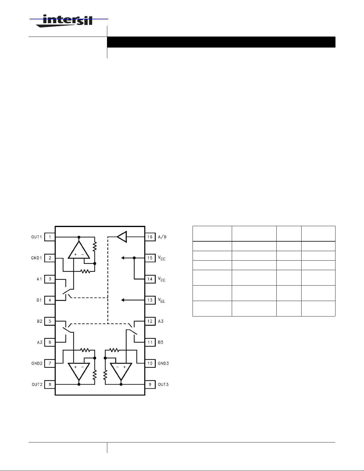
Pinout
EL4332
[16-PIN SO (0.150”)]
TOP VIEW
FN7163.2
Features
• 3ns A-B switching
• 300MHz bandwidth
• Fixed gain of 2, for cable driving
• > 650V/µs slew rate
• TTL/CMOS compatible switch
• Pb-free available
Applications
• RGB multiplexing
• Picture-in-picture
• Cable driving
• HDTV processing
• Switched gain amplifiers
• ADC input multiplexer
Ordering Information
PART NUMBER PACKAGE
EL4332CS 16-Pin SO (0.150”) - MDP0027
EL4332CS-T7 16-Pin SO (0.150”) 7” MDP0027
EL4332CS-T13 16-Pin SO (0.150”) 13” MDP0027
EL4332CSZ
(Note)
EL4332CSZ-T7
(Note)
EL4332CSZ-T13
(Note)
NOTE: Intersil Pb-free products employ special Pb-free material
sets; molding compounds/die attach materials and 100% matte tin
plate termination finish, which is compatible with both SnPb and
Pb-free soldering operations. Intersil Pb-free products are MSL
classified at Pb-free peak reflow temperatures that meet or exceed
the Pb-free requirements of IPC/JEDEC J Std-020B.
16-Pin SO (0.150”)
(Pb-Free)
16-Pin SO (0.150”)
(Pb-Free)
16-Pin SO (0.150”)
(Pb-Free)
TAPE &
REEL PKG. DWG. #
- MDP0027
7” MDP0027
13” MDP0027
Demo Board
A demo PCB is available for this product.
1
Copyright © Intersil Americas Inc. 2002-2004. All Rights Reserved. Elantec is a registered trademark of Elantec Semiconductor, Inc.
CAUTION: These devices are sensitive to electrostatic discharge; follow proper IC Handling Procedures.
1-888-INTERSIL or 321-724-7143
| Intersil (and design) is a registered trademark of Intersil Americas Inc.
All other trademarks mentioned are the property of their respective owners.
EL4332
Absolute Maximum Ratings (T
V
to VEE . . . . . . . . . . . . . . . . . . . . . . . . . . . . . . . . . . . . . . . . .14V
CC
V
to any GND . . . . . . . . . . . . . . . . . . . . . . . . . . . . . . . . . . . . .12V
CC
V
to any GND . . . . . . . . . . . . . . . . . . . . . . . . . . . . . . . . . . . . .12V
EE
Continuous Output Current . . . . . . . . . . . . . . . . . . . . . . . . . . . 45mA
Any Input . . . . . . . . . . . . . . . . . . . . . . . . . . V
CAUTION: Stresses above those listed in “Absolute Maximum Ratings” may cause permanent damage to the device. This is a stress only rating and operation of the
device at these or any other conditions above those indicated in the operational sections of this specification is not implied.
IMPORTANT NOTE: All parameters having Min/Max specifications are guaranteed. Typical values are for information purposes only. Unless otherwise noted, all tests
are at the specified temperature and are pulsed tests, therefore: T
DC Electrical Specifications V
= 25°C)
A
Input Current, Any Input. . . . . . . . . . . . . . . . . . . . . . . . . . . . . . . 5mA
Power Dissipation . . . . . . . . . . . . . . . . . . . . . . . . . . . . . See Curves
Ambient Operating Temperature. . . . . . . . . . . . . . . . .-40°C to 85°C
Junction Temperature . . . . . . . . . . . . . . . . . . . . . . . . . . . . . . .150°C
-0.3V to VCC +0.3V
EE
= TC = T
J
= +5V, VEE = -5V, Temperature = 25°C, RL = ∞
CC
A
Storage Temperature. . . . . . . . . . . . . . . . . . . . . . . .-60°C to +150°C
PARAMETER DESCRIPTION MIN TYP MAX UNITS
V
dV
R
I
B
dI
A
dA
C
OS
OS
IN
B
V
V
IN
Input Referred Offset Voltage 8 20 mV
Input Referred Offset Voltage Delta (Note 1) 2 8 mV
Input Resistance 30 kΩ
Input Bias Current -7 -30 µA
Input Bias Current Delta (Note 1) 0.5 4.0 µA
Gain 1.94 2.00 2.06 V/V
Gain Delta (Note 1) 0.5 2.5 %
Input Capacitance 3.3 pF
PSRR Power Supply Rejection Ratio 50 70 dB
V
O
Output Voltage Swing into 500Ω load ±2.7 ±3.6 V
Output Voltage Swing into 150Ω load +3/-2.7 V
I
OUT
Xtalk
Xtalk
V
IH
V
IL
I
IL
I
IH
I
S
AB
CH-CH
Current Output, Measured with 75Ω Load (Note 2) 30 40 mA
Crosstalk from Non-selected Input (at DC) -70 -100 dB
Crosstalk from one Amplifier to another Amplifier -70 -100 dB
Input Logic High Level 2.0 V
Input Logic Low Level 0.8 V
Logic Low Input Current (VIN = 0V) -0.3 -40 -80 µA
Logic High Input Current (VIN = 0V) -3 0 3 µA
Total Supply Current 38 48 60 mA
NOTES:
1. Each channel’s A-input to its B-input.
2. There is no short circuit protection on any output.
AC Electrical Specifications V
= +5V, VEE = -5V, Temperature = 25°C, RL = 150Ω, CL = 3pF.
CC
PARAMETER DESCRIPTION MIN TYP MAX UNITS
BW -3dB Bandwidth 300 MHz
BW 0.1dB ±0.1dB Bandwidth 105 MHz
DG Differential Gain at 3.58MHz 0.04 %
DP Differential Phase at 3.58MHz 0.08 °
Pkg Peaking with Nominal Load 0.2 dB
SR Slew Rate (4V Square Wave, Measured 25%–75%) 650 V/µs
2
EL4332
AC Electrical Specifications V
PARAMETER DESCRIPTION MIN TYP MAX UNITS
t
S
T
SW
OS Overshoot, V
ab 10M Input to Input Isolation at 10MHz 60 dB
I
SO
100M Input to Input Isolation at 100MHz 40 dB
I
ch-ch 10M Channel to Channel Isolation at 10MHz 61 dB
SO
100M Channel to Channel Isolation at 100MHz 50 dB
Settling Time to 0.1% of Final Value 13 ns
Time to Switch Inputs 3 ns
= +5V, VEE = -5V, Temperature = 25°C, RL = 150Ω, CL = 3pF. (Continued)
CC
= 4V
OUT
P-P
8%
Pin Descriptions
PIN NAME FUNCTION
A1, A2, A3 “A” inputs to amplifiers 1, 2 and 3 respectively.
B1, B2, B3 “B” inputs to amplifiers 1, 2 and 3 respectively.
GND1, GND2, GND3 These are the individual ground pins for each channel.
Out1, Out2, Out3 Amplifier outputs. Note: there is no short circuit protection on any output.
V
CC
V
EE
A/B Common input select pin, a logic high selects the “A” inputs, logic low selects the “B” inputs. CMOS/TTL
Positive power supply. Typically +5V.
Negative power supply. Typically -5V.
compatible.
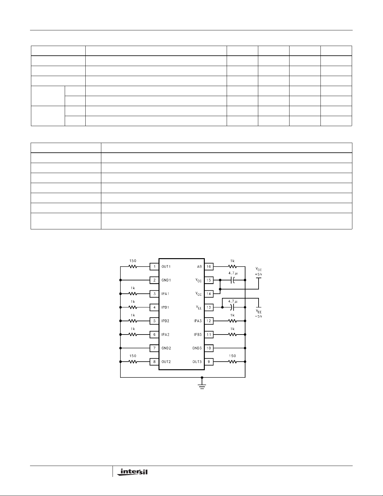
Burn In Schematic
3
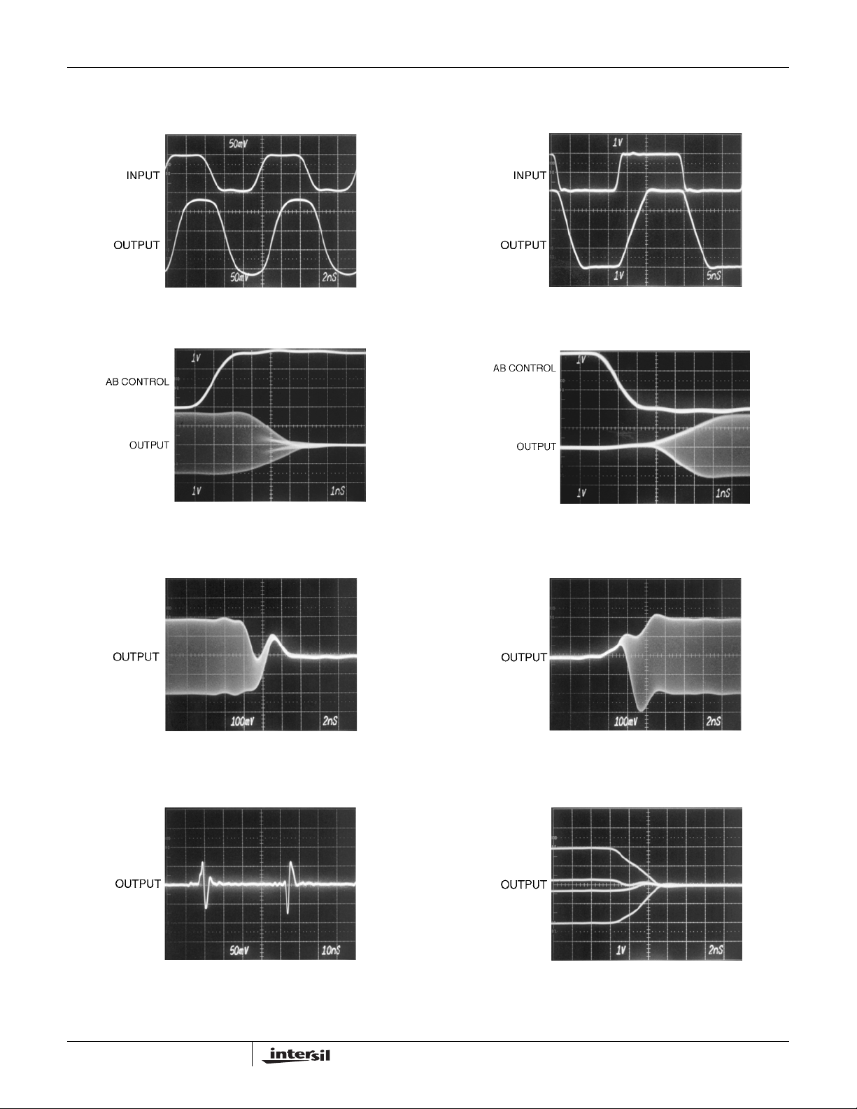
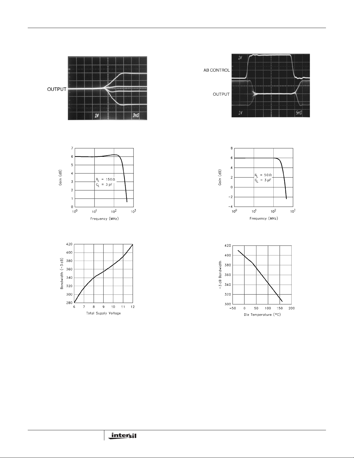
Typical Performance Curves
EL4332
FIGURE 1. SMALL SIGNAL TRANSIENT RESPONSE
FIGURE 3. SWITCHING TO GROUND FROM A LARGE
SIGNAL UNCORRELATED SINE WAVE
FIGURE 2. LARGE SIGNAL TRANSIENT RESPONSE
FIGURE 4. SWITCHING FROM GROUND TO A LARGE
SIGNAL UNCORRELATED SINE WAVE
FIGURE 5. SWITCHING TO GROUND FROM A SMALL
SIGNAL UNCORRELATED SINE WAVE
FIGURE 7. SWITCHING GLITCH (INPUTS AT GROUND)
4
FIGURE 6. SWITCHING FROM GROUND TO A SMALL
SIGNAL UNCORRELATED SINE WAVE
FIGURE 8. SWITCHING FROM A FAMILY OF DC LEVELS TO
GROUND
Typical Performance Curves (Continued)
EL4332
FIGURE 9. SWITCHING FROM GROUND TO A FAMILY OF DC
LEVELS
FIGURE 11. GAIN vs FREQUENCY FIGURE 12. GAIN vs FREQUENCY
FIGURE 10. CHANNEL A/B SWITCHING DELAY
FIGURE 13. -3dB BW vs SUPPLY VOLTAGE
5
FIGURE 14. BANDWIDTH vs DIE TEMPERATURE

Typical Performance Curves (Continued)
EL4332
FIGURE 15. FREQUENCY RESPONSE WITH CAPACITIVE
LOADS
FIGURE 17. A-INPUT TO B–INPUT ISOLATION FIGURE 18. CHANNEL-CHANNEL ISOLATION
FIGURE 16. INPUT VOLTAGE NOISE OVER FREQUENCY
FIGURE 19. OUTPUT SWING vs SUPPLY VOLTAGE
6
FIGURE 20. OUTPUT SWING vs FREQUENCY

Typical Performance Curves (Continued)
EL4332
FIGURE 21. SLEW RATE vs SUPPLY VOLTAGE
FIGURE 23. SUPPLY CURRENT vs SUPPLY VOLTAGE
JEDEC JESD51-7 HIGH EFFECTIVE
THERMAL CONDUCTIVITY TEST BOARD
1.8
1.6
1.563W
1.4
1.2
1
0.8
0.6
0.4
POWER DISSIPATION (W)
0.2
0
0 255075100 150
FIGURE 25. POWER DISSIPATION vs AMBIENT TEMPERATURE
FIGURE 22. SLEW RATE vs DIE TEMPERATURE
FIGURE 24. POWER DISSIPATION vs AMBIENT
S
O
16
θ
(
0.
J
A
150”
=
80°
)
C
/
W
12585
AMBIENT TEMPERATURE (°C)
JEDEC JESD51-3 LOW EFFECTIVE
THERMAL CONDUCTIVITY TEST BOARD
1.2
1.136W
1
0.8
0.6
0.4
0.2
POWER DISSIPATION (W)
0
0 255075100 150
S
O
1
6
θ
(
J
0
A
=
.
1
1
5
1
0
0
”
°
)
C
/
W
12585
AMBIENT TEMPERATURE (°C)
TEMPERATURE
7

EL4332
FIGURE 26. TYPICAL CONNECTION FOR A 2:1 COMPONENT VIDEO MULTIPLEXER
Applications Information
Figure 26 shows a typical use for the EL4332. The circuit is a
component video (R,G, B or Y,U,V) multiplexer. Since the
gain of the internal amplifiers has been set to 2, the only
extra components needed are the supply decoupling
capacitors and the back terminating resistors, if transmission
lines are to be driven. The EL4332 can drive backmatched
50Ω or 75Ω loads.
Grounds
It will be noticed that each mux-amp channel has its own
separate ground pin. These g ro und pins have been kept
separate to keep the channel separation inside the chip as
large as possible. The feedback resistors use these ground
pins as their reference. The resistors total 400Ω, so there is
a significant signal current flowing from these pins to ground.
The ground pins should all be connected together, to a
ground plane underneath the chip. 1 oz. copper for the
ground plane is highly recommended.
Further notes and recommended practices for high speed
printed circuit board layout can be found in the tutorials in
the Elantec databooks.
Supplies
Supply bypassing should be as physically near the power
pins as possible. Chip capacitors should be used to
minimize lead inductance. Note that larger values of
capacitor tend to have larger internal inductances. So when
designing for 3 transmission lines or similar moderate loads,
a 0.1µF ceramic capacitor right next to the power pin in
parallel with a 22µF tantalum capacitor placed as close to
the 0.1µF is recommended. For lighter loadings, or if not all
the channels are being used, a single 4.7µF capacitor has
been found quite adequate.
Note that component video signals do tend to have a high
level of signal correlation. This is especially true if the video
signal has been derived from 3 synchronously clocked
DACs. This corresponds to all three channels drawing large
slew currents simultaneously from the supplies. Thus, proper
bypassing is critical.
8

Logic Inputs
The A/B select, logic input, is internally referenced to
ground. It is set at 2 diode drops above ground, to give a
threshold of about 1.4V (see Figure 27). The PNP input
transistor requires that the driving gate be able to sink
current, typically < 30µA, for a logic “low”. If left to float, it will
be a logic “high”.
FIGURE 27. SIMPLIFIED LOGIC INPUT STAGE
EL4332
The input PNP transistors have sufficient gain that a simple
level shift circuit (see Figure 28) can be used to provide a
simple interface with Emitter Coupled Logic. Typically,
200mV is enough to switch from a solid logic “low” to a
“high.”
FIGURE 28. ADAPTING THE SELECT PIN
The capacitor C
FOR ECL LOGIC LEVELS
is only in the network to prevent the A/B
FF
pin’s capacitance from slowing the control signal. The
network shown level shifts the ECL levels, -0.7V to -1.5V to
+1.6V and +1.1V respectively. The terminating resistor, R
TT
is required since the open emitter of the ECL gate can not
sink current. If a -2V rail is not being used, a 220Ω to 330Ω
resistor to the -5.2V rail would have the same effect.
,
9

EL4332
Expanding the Multiplexer
In Figure 29, a 3:1 multiplexer circuit is shown. The
expansion to more inputs is very straight forward. Since the
EL4332 has a fixed gain of 2, interstage attenuators may be
required as shown in Figure 28. The truth table for the 3:1
multiplexer select lines is:
TABLE 1.
XY MUX OUTPUT
0 0 R3, G3, B3
0 1 R2, G2, B2
1 X R1, G1, B1
When interstage attenuators are used, the values should be
kept down in the region of 50Ω–300Ω. This is to prevent a
combination of circuit board stray capacitance and the
EL4332’s input capacitance forming a significant pole. For
example, if instead of 100Ω as shown, resistors of 1kΩ had
been used, and assuming 3pF of stray and 3pF of input
capacitance, a pole would be formed at about 53MHz.
FIGURE 29. TYPICAL CONNECTION FOR A 3:1 COMPONENT VIDEO MULTIPLEXER
10

EL4332
A Bandwidth Selectable Circuit
In Figure 30, a circuit is shown that allows three signals to be
either low pass filtered or full bandwidth.
This could be useful where an input signal is frequently
noisy. The component values shown give a Butterworth LPF
response, with a -3dB frequency of 50MHz. Note again, the
resistor values are low, so that stray capacitance does not
affect the desired cut-off frequency.
FIGURE 30. SWITCHED 50MHz LOW PASS FILTER FOR HIGH/LOW RESOLUTION MONITORS
11

EL4332
EL4332 Macromodel
* EL4332 Macromodel
* Revision A, April 1996
****************************************************************************
*Applications Hints. The EL4332 has two V
*pins. The VCC pins (pins 14 and 15 are internally shorted together in the model,
*but the ground pins (GND1, GND2, and GND3 (nodes 2, 7, and 10, respectively)
*must be connected to ground (node 0) using a le-6W resistor. Alternatively,
* nodes 2, 7, and 10 may be connected to ground through a 25Ω resistor in parallel
* with a 4nH inductor to simulate package and PCB parasitics.
****************************************************************************
* Connections:
* OUT1
* | GND1
* | | A1
* | | | B1
* | | | | B2
* | | | | | A2
* | | | | | | GND2
* | | | | | | | OUT2
* | | | | | | | |
* | | | | | | | |
* 1 2 3 4 5 6 7 8
*
* OUT3
* | GND3
* | | B3
* | | | A3
* | | | | V
* | | | | | V
* | | | | | | V
* | | | | | | | A/B
* | | | | | | | |
* | | | | | | | |
* 9 10 11 12 13 14 15 16
************A B Switch ***************
Rshort 14 15 le-12
rshort1 15 0 100 Meg
Isw 14 110 1.5 mA
vref 111 0 1.6V
q1 101 16 110 qp
q2 102 111 110 qp
R1 101 13 500
R2 102 13 500
Rd1 107 0 100
Esw 107 0 table {v(102, 101)*100} (0,0) (1,1)
*
************Amplifier #1 *************
q131 103 3 112 qp
q141 104 114 113 qp
q151 105 4 115 qp
q161 106 117 116 qp
Ia11 14 112 1 mA
Ia21 14 113 1 mA
Ib11 14 115 1 mA
Ib21 14 116 1 mA
Rga1 112 113 275
Rgb1 115 116 275
R31 103 13 275
R41 104 13 275
EE
CC
CC
pins, one VEE pin, and three ground
CC
12

EL4332
R51 105 13 275
R61 106 13 275
R71 1 114 400
R81 114 2 400
R911 117 400
R110 117 2 400
Ediff1 108 0 value {(v(104,103)*v(107))+(v(106,105)*(1-v(107)))}
rdiff1 108 0 1K
*
*Compensation Section
*
ga1 0 134 108 0 1m
rh1 134 0 5 Meg
cc1 134 0 0.6 pF
*
*Poles
*
ep1 141 0 134 0 1.0
rpa1 141 142 200
cpa1 142 0 0.75 pF
rpb1 142 143 200
cpb1 143 0 0.75 pF
*
*Output Stage
*
i011 15 150 1.0 mA
i021 151 13 1.0 mA
q71 13 143 150 qp
q81 15 143 151 qn
q91 15 150 152 qn
q101 13 151 153 qp
ros11 152 1 2
ros21 153 1 2
*
************Amplifier #2***********
q231 203 6 212 qp
q241 204 214 213 qp
q251 205 5 215 qp
q261 206 217 216 qp
Ia12 14 212 1 mA
Ia22 14 213 1 mA
Ib12 14 215 1 mA
Ib22 14 216 1 mA
Rga2 212 213 275
Rgb2 215 216 275
R231 203 13 275
R241 204 13 275
R251 205 13 275
R261 206 13 275
R271 8 214 400
R281 214 7 400
R291 8 217 400
R210 217 7 400
Ediff2 208 0 value {(v(204,203)*v(107))+(v(206,205)*(1-v(107)))}
rdiff2 208 0 1K
*
* Compensation Section
*
ga2 0 234 208 0 1m
rh2 234 0 5 Meg
cc2 234 0 0.6 pF
13

EL4332
*
* Poles
*
ep2 241 0 234 0 1.0
rpa2 241 242 200
cpa2 242 0 0.75 pF
rpb2 242 243 200
cpb2 243 0 0.75 pF
*
*Output Stage
*
i0 12 15 250 1.0 mA
i022 251 13 1.0 mA
q271 13 243 250 qp
q281 15 243 251 qn
q291 15 250 252 qn
q201 13 251 253 qp
ros12 252 8 2
ros22 253 8 2
*
************Amplifier #3 ************
q331 303 12 312 qp
q341 304 314 313 qp
q351 305 11 315 qp
q361 306 317 316 qp
Ia13 14 312 1 mA
Ia23 14 313 1 mA
Ib13 14 315 1 mA
Ib23 14 316 1 mA
Rga3 312 313 275
Rgb3 315 316 275
R331 303 13 275
R341 304 13 275
R351 305 13 275
R361 306 13 275
R371 9 314 400
R381 314 10 400
R391 9 317 400
R310 317 10 400
Ediff3 308 0 value {( v(304,303)*(v(107))+(v(306,305)*(1-v(107)))}
rdiff3 308 0 1K
*
* Compensation
*
ga3 0 334 308 01m
rh3 334 0 5 Meg
cc3 334 0 0.6 pF
*
* Poles
*
ep3 341 0 3340 1.0
rpa3 341 342 200
cpa3 342 0 0.75 pF
rpb3 342 343 200
cpb3 343 0 0.75 pF
*
* Output Stage
*
i013 15 350 1.0 mA
i023 351 13 1.0 mA
q371 13 343 350 qp
14

q381 15 343 351 qn
q391 15 350 352 qn
q301 13 351 353 qp
ros13 352 9 2
ros23 353 9 2
*
* Power Supply Current
*
ips 15 13 22 mA
*
*Models
*
.model qp pnp(is=1.5e-16 bf=300 tf=0.01 ns)
.model qn npn(is=0.8e-18 bf=300 tf=0.01 ns)
.ends
EL4332
All Intersil U.S. products are manufactured, assembled and tested utilizing ISO9000 quality systems.
Intersil Corporation’s quality certifications can be viewed at www.intersil.com/design/quality
Intersil products are sold by description only. Intersil Corporation reserves the right to make changes in circuit design, software and/or specifications at any time without
notice. Accordingly, the reader is cautioned to verify that data she ets are current before placin g orders. Information furn ished by Intersil is believed to be accurate and
reliable. However, no responsibility is assumed by Intersil or its subsidiaries for its use; nor for any infringements of patents or other rights of third parties which may result
from its use. No license is granted by implication or othe rwise under any patent or patent rights of Intersil or its subsidiaries.
For information regarding Intersil Corporation and its products, see www.intersil.com
15
 Loading...