

Page 1
www.BDTIC.com/Intersil
®
EL1516, EL1516A
Data Sheet
Dual Ultra Low Noise Amplifier
The EL1516 is a dual, ultra low noise amplifier, ideally suited
to line receiving applications in ADSL, VDSL, and home
PNA designs. With low noise specification of just 1.3nV/√Hz
and 1.5pA/√Hz, the EL1516 is perfect for the detection of
very low amplitude signals.
The EL1516 features a -3dB bandwidth of 350MHz @ A
=-1
V
and is gain-of-2 stable. The EL1516 also affords minimal
power dissipation with a supply current of just 5.5mA per
amplifier. The amplifier can be powered from supplies ranging
from 5V to 12V.
The EL1516A incorporates an enable and disable function to
reduce the supply current to 5nA typical per amplifier,
allowing the EN
pins to float or apply a low logic level will
enable the amplifiers.
The EL1516 is available in space-saving 8 Ld MSOP and
industry-standard 8 Ld SOIC packages and the EL1516A is
available in a 10 Ld MSOP package. All are specified for
operation over the -40°C to +85°C temperature range.
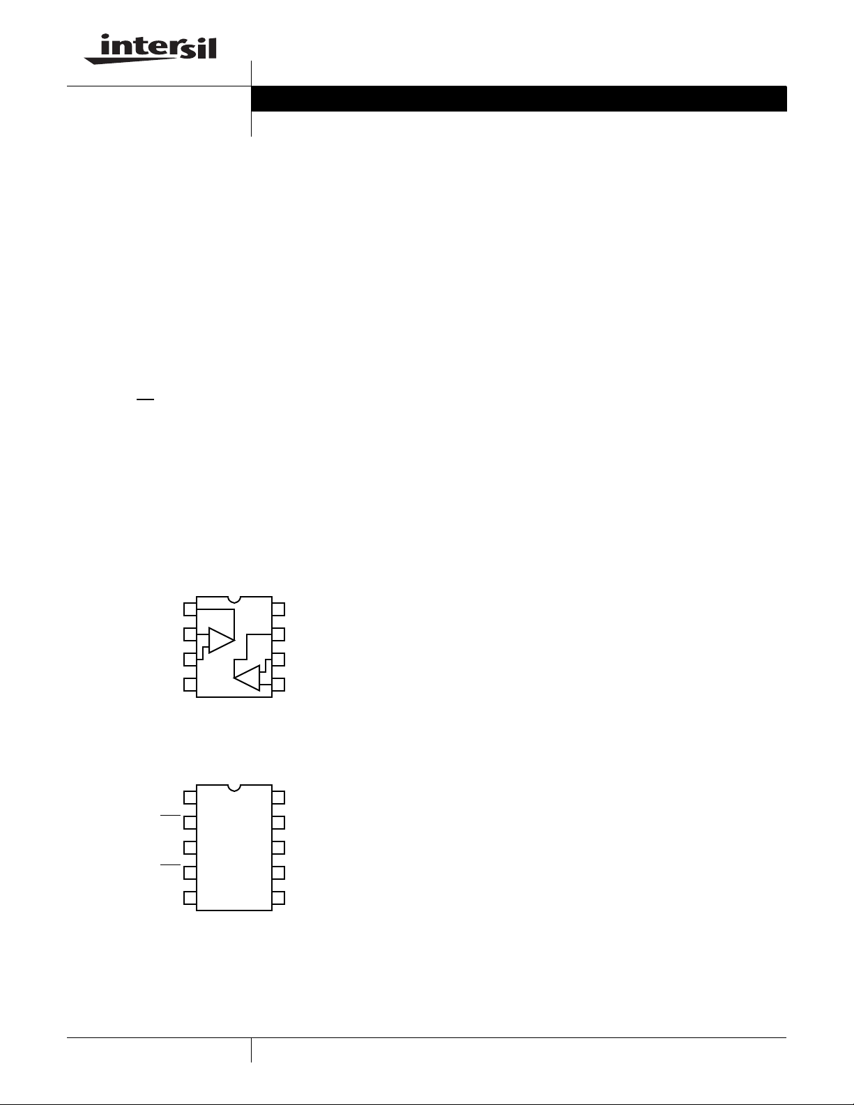
Pinouts
EL1516
(8 LD SOIC, 8 LD MSOP)
TOP VIEW
VOUTA
VINA-
VINA+
VS-
1
2
-
+
3
4
8
VS+
VOUTB
7
VINB-
6
-
+
VINB+
5
May 3, 2007
FN7328.2
Features
• EL2227 upgrade replacement
• Voltage noise of only 1.3nV/√Hz
• Current noise of only 1.5pA/√Hz
• Bandwidth (-3dB) of 350MHz @ A
• Bandwidth (-3dB) of 250MHz @ A
= -1
V
= +2
V
• Gain-of-2 stable
• Just 5.5mA per amplifier
•100mA I
OUT
• Fast enable/disable (EL1516A only)
• 5V to 12V operation
• Pb-free plus anneal available (RoHS compliant)
Applications
• ADSL receivers
• VDSL receivers
• Home PNA receivers
• Ultrasound input amplifiers
• Wideband instrumentation
• Communications equipment
• AGC and PLL active filters
• Wideband sensors
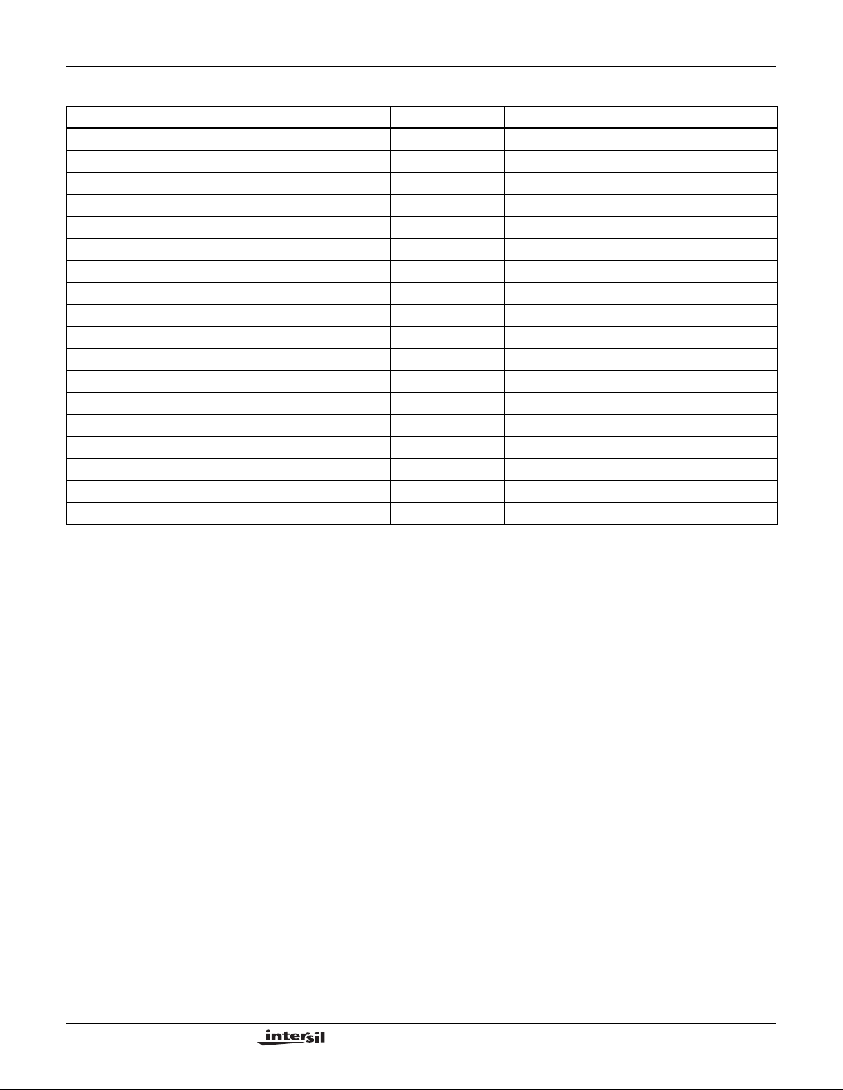
EL1516A
(10 LD MSOP)
TOP VIEW
VINA+
1
ENA
2
VS-
3
ENB VOUTB
4
VINB+
5 6
10
VINA-
VOUTA
9
VS+
8
7
VINB-
1
CAUTION: These devices are sensitive to electrostatic discharge; follow proper IC Handling Procedures.
1-888-INTERSIL or 1-888-468-3774
| Intersil (and design) is a registered trademark of Intersil Americas Inc.
Copyright © Intersil Americas Inc. 2005, 2006, 2007. All Rights Reserved.
All other trademarks mentioned are the property of their respective owners.
Page 2
www.BDTIC.com/Intersil
EL1516, EL1516A
Ordering Information
PART NUMBER PART MARKING TAPE AND REEL PACKAGE PKG. DWG. #
EL1516IY BAAHA - 8 Ld MSOP (3.0mm) MDP0043
EL1516IY-T13 BAAHA 13” 8 Ld MSOP (3.0mm) MDP0043
EL1516IY-T7 BAAHA 7” 8 Ld MSOP (3.0mm) MDP0043
EL1516IYZ (Note) BAAAY - 8 Ld MSOP (Pb-free) (3.0mm) MDP0043
EL1516IYZ-T13 (Note) BAAAY 13” 8 Ld MSOP (Pb-free) (3.0mm) MDP0043
EL1516IYZ-T7 (Note) BAAAY 7” 8 Ld MSOP (Pb-free) (3.0mm) MDP0043
EL1516IS 1516IS - 8 Ld SOIC (150 mil) MDP0027
EL1516IS-T13 1516IS 13” 8 Ld SOIC (150 mil) MDP0027
EL1516IS-T7 1516IS 7” 8 Ld SOIC (150 mil) MDP0027
EL1516ISZ (Note) 1516ISZ - 8 Ld SOIC (Pb-free) (150 mil) MDP0027
EL1516ISZ-T13 (Note) 1516ISZ 13” 8 Ld SOIC (Pb-free) (150 mil) MDP0027
EL1516ISZ-T7 (Note) 1516ISZ 7” 8 Ld SOIC (Pb-free) (150 mil) MDP0027
EL1516AIY BBDAA - 10 Ld MSOP (3.0mm) MDP0043
EL1516AIY-T13 BBDAA 13” 10 Ld MSOP (3.0mm) MDP0043
EL1516AIY-T7 BBDAA 7” 10 Ld MSOP (3.0mm) MDP0043
EL1516AIYZ (Note) BBEAA - 10 Ld MSOP (Pb-free) (3.0mm) MDP0043
EL1516AIYZ-T13 (Note) BBEAA 13” 10 Ld MSOP (Pb-free) (3.0mm) MDP0043
EL1516AIYZ-T7 (Note) BBEAA 7” 10 Ld MSOP (Pb-free) (3.0mm) MDP0043
NOTE: Intersil Pb-free plus anneal products employ special Pb-free material sets; molding compounds/die attach materials and 100% matte tin plate
termination finish, which are RoHS compliant and compatible with both SnPb and Pb-free soldering operations. Intersil Pb-free products are MSL
classified at Pb-free peak reflow temperatures that meet or exceed the Pb-free requirements of IPC/JEDEC J STD-020.
2
FN7328.2
May 3, 2007
Page 3
www.BDTIC.com/Intersil
EL1516, EL1516A
Absolute Maximum Ratings (T
Supply Voltage between VS+ and VS-. . . . . . . . . . . . . . . . . . . . .14V
Input Voltage . . . . . . . . . . . . . . . . . . . . . . . . . . .V
Maximum Continuous Output Current . . . . . . . . . . . . . . . . . . . 40mA
Maximum Die Temperature . . . . . . . . . . . . . . . . . . . . . . . . . .+150°C
= +25°C) Thermal Information
A
Storage Temperature. . . . . . . . . . . . . . . . . . . . . . . .-65°C to +150°C
- -0.3V, VS +0.3V
S
Operating Temperature . . . . . . . . . . . . . . . . . . . . . . .-40°C to +85°C
Power Dissipation . . . . . . . . . . . . . . . . . . . . . . . . . . . . . See Curves
Pb-free reflow profile . . . . . . . . . . . . . . . . . . . . . . . . . .see link below
http://www.intersil.com/pbfree/Pb-FreeReflow.asp
CAUTION: Stresses above those listed in “Absolute Maximum Ratings” may cause permanent damage to the device. This is a stress only rating and operation of the
device at these or any other conditions above those indicated in the operational sections of this specification is not implied.
IMPORTANT NOTE: All parameters having Min/Max specifications are guaranteed. Typ values are for information purposes only. Unless otherwise noted, all tests are
at the specified temperature and are pulsed tests, therefore: T
Electrical Specifications V
= +2.5V, VS- = -2.5V, RL = 500Ω and CL = 3pF to 0V, RF = RG = 620Ω, VCM = 0V, and TA = +25°C,
S+
Unless Otherwise Specified.
= TC = T
J
A
PARAMETER DESCRIPTION CONDITIONS MIN TYP MAX UNIT
INPUT CHARACTERISTICS
V
OS
TCV
I
B
I
OS
R
IN
C
IN
OS
Input Offset Voltage V
Average Offset Voltage Drift -0.3 µV/°C
Input Bias Current V
Input Offset Current 50 500 nA
Input Impedance 2MΩ
Input Capacitance 1.6 pF
= 0V -0.2 +3 mV
CM
= 0V 6.5 9 µA
CM
CMIR Common-Mode Input Range -1.3 +1.7 V
CMRR Common-Mode Rejection Ratio for V
A
e
i
VOL
n
n
Open-Loop Gain VO = ±1.25V 70 75 dB
Voltage Noise f = 100kHz 1.24 nV/√Hz
Current Noise f = 100kHz 1.5 pA/√Hz
from -4.7V to 5.4V 85 105 dB
IN
OUTPUT CHARACTERISTICS
V
V
I
OL
OH
SC
Output Swing Low RL = 500Ω 1.45 1.35 V
= 150Ω 1.37 1.25 V
R
L
Output Swing High RL = 500Ω 1.5 1.6 V
= 150Ω 1.4 1.5 V
R
L
Short Circuit Current RL = 10Ω 60 75 mA
POWER SUPPLY PERFORMANCE
PSRR Power Supply Rejection Ratio V
I
S ON
I
S OFF
TC I
V
S
S
Supply Current Enable (Per Amplifier) No load 5.7 7 mA
Supply Current Disable (Per Amplifier)
(EL1516A)
IS Temperature Coefficient 32 µA/°C
Operating Range 512V
is moved from ±5.4V to ±6.6V 75 80 dB
S
I+ (DIS) 2 20 µA
I- (DIS) -21 -16 µA
DYNAMIC PERFORMANCE
SR Slew Rate V
= ±1.25V square wave, measured 25% to 75% 80 1 10 V/µs
O
TC SR SR Temperature Coefficient 0.5 V/µs/°C
t
S
Settling to 0.1% (AV = +2) AV = +2, V
BW1 -3dB Bandwidth A
BW2 -3dB Bandwidth A
= -1, R
V
= +2, R
V
±1V 25 ns
O =
100Ω 320 MHz
F =
100Ω 200 MHz
F =
3
FN7328.2
May 3, 2007
Page 4
www.BDTIC.com/Intersil
EL1516, EL1516A
Electrical Specifications V
PARAMETER DESCRIPTION CONDITIONS MIN TYP MAX UNIT
HD2 2nd Harmonic Distortion f = 1MHz, VO = 2V
HD3 3rd Harmonic Distortion f = 1MHz, V
ENABLE (EL1516AIY ONLY)
t
EN
t
DIS
I
IHEN
I
ILEN
V
IHEN
V
IHEN
Enable Time 125 ns
Disable Time 336 ns
EN Pin Input High Current EN = VS+18µA
EN Pin Input Low Current EN = VS-10nA
EN Pin Input High Voltage for
Power-down
EN Pin Input Low Voltage for Power-up VS- +3 V
Electrical Specifications V
PARAMETER DESCRIPTION CONDITIONS MIN TYP MAX UNIT
INPUT CHARACTERISTICS
V
OS
TCV
OS
I
B
I
OS
R
IN
C
IN
CMIR Common-Mode Input Range -4.5 +5.5 V
CMRR Common-Mode Rejection Ratio for V
A
VOL
e
n
i
n
OUTPUT CHARACTERISTICS
V
OL
V
OH
I
SC
POWER SUPPLY PERFORMANCE
PSRR Power Supply Rejection Ratio V
I
S ON
I
S OFF
TC I
S
V
S
Input Offset Voltage V
Average Offset Voltage Drift -0.3 µV/°C
Input Bias Current V
Input Offset Current 50 500 nA
Input Impedance 12 MΩ
Input Capacitance 1.6 pF
Open-Loop Gain VO = ±2.5V 75 80 dB
Voltage Noise f = 100kHz 1.24 nV/√Hz
Current Noise f = 100kHz 1.5 pA/√Hz
Output Swing Low RL = 500Ω -4.8 -4.7 V
Output Swing High RL = 500Ω 4.8 4.9 V
Short Circuit Current RL = 10Ω 110 160 mA
Supply Current Enable (Per Amplifier) No load 5.8 7 mA
Supply Current Disable (Per Amplifier)
(EL1516A)
IS Temperature Coefficient 32 µA/°C
Operating Range 512V
= +2.5V, VS- = -2.5V, RL = 500Ω and CL = 3pF to 0V, RF = RG = 620Ω, VCM = 0V, and TA = +25°C,
S+
Unless Otherwise Specified. (Continued)
, RL = 100Ω 90 dBc
P-P
= 2V
O
= +6V, VS- = -6V, RL = 500Ω and CL = 3pF to 0V, RF = RG = 620Ω, VCM = 0V, and TA = +25°C,
S+
Unless Otherwise Specified.
= 0V 0.1 3 mV
CM
= 0V 6.5 9 µA
CM
from -4.7V to 5.4V 90 110 dB
IN
= 150Ω -4.6 -4.5 V
R
L
= 150Ω 4.5 4.7 V
R
L
is moved from ±5.4V to ±6.6V 75 85 dB
S
I+ (DIS) 2 5 µA
I- (DIS) -19 -16 µA
, RL = 100Ω 95 dBc
P-P
VS+ -1 V
4
FN7328.2
May 3, 2007
Page 5
www.BDTIC.com/Intersil
EL1516, EL1516A
Electrical Specifications V
= +6V, VS- = -6V, RL = 500Ω and CL = 3pF to 0V, RF = RG = 620Ω, VCM = 0V, and TA = +25°C,
S+
Unless Otherwise Specified. (Continued)
PARAMETER DESCRIPTION CONDITIONS MIN TYP MAX UNIT
DYNAMIC PERFORMANCE
SR Slew Rate V
= ±2.5V square wave, measured 25% to 75% 90 128 V/µs
O
TC SR SR Temperature Coefficient 0.5 V/µs/°C
t
S
BW1 -3dB Bandwidth A
Settling to 0.1% (AV = +2) AV = +2, V
= -1, R
V
BW2 -3dB Bandwidth AV = +2, R
HD2 2nd Harmonic Distortion f = 1MHz, V
f = 1MHz, V
HD3 3rd Harmonic Distortion f = 1MHz, VO = 2V
f = 1MHz, V
±1V 20 ns
O =
100Ω 350 MHz
F =
100Ω 250 MHz
F =
= 2V
O
O
O
, RL = 500Ω 12 5 dBc
P-P
= 2V
, RL = 150Ω 117 dBc
P-P
, RL = 500Ω 115 dBc
P-P
= 2V
, RL = 150Ω 110 dBc
P-P
ENABLE (EL1516AIY ONLY)
t
EN
t
DIS
I
IHEN
I
ILEN
V
IHEN
V
IHEN
Enable Time 125 ns
Disable Time 336 ns
EN Pin Input High Current EN = VS+1720µA
EN Pin Input Low Current EN = VS- 7 20 nA
EN Pin Input High Voltage for
VS+ -1 V
Power-down
EN Pin Input Low Voltage for Power-up VS- +3 V
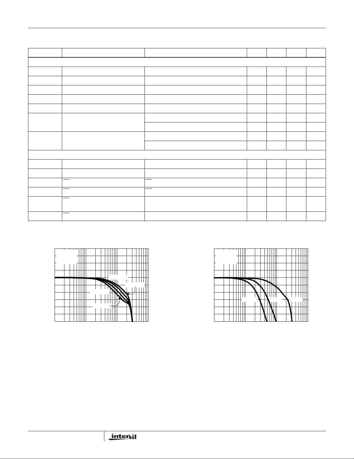
Typical Performance Curves
4
VS = ±6V
= +2
A
V
= 500Ω
R
L
2
0
-2
-4
NORMALIZED GAIN (dB)
-6
1M 1G10M
FREQUENCY (Hz)
FIGURE 1. NON-INVERTING FREQUENCY RESPONSE FOR
VARIOUS R
F
RF = 100Ω
RF = 348Ω
RF = 1kΩ
RF = 619Ω
100M
4
VS = ±6V
= 348Ω
R
F
= 500Ω
R
L
2
0
-2
AV = 10 AV = 5 AV = 2
-4
NORMALIZED GAIN (dB)
-6
1M 1G10M
FREQUENCY (Hz)
100M
FIGURE 2. NON-INVERTING FREQUENCY RESPONSE (GAIN)
5
FN7328.2
May 3, 2007
Page 6
www.BDTIC.com/Intersil
Typical Performance Curves (Continued)
EL1516, EL1516A
4
VS = ±6V
A
V
R
L
2
R
F
0
-2
-4
NORMALIZED GAIN (dB)
-6
1M 1G10M
= +2
= 500Ω
= 619Ω
CL = 12pF
CL = 4.7pF
CL = 1pF
CL = 0pF
FREQUENCY (Hz)
CL = 22pF
100M
FIGURE 3. NON-INVERTING FREQUENCY RESPONSE FOR
NORMALIZED GAIN (dB)
VARIOUS C
4
VS = ±6V
A
V
R
L
2
R
F
0
V
IN
-2
-4
= +2
= 500Ω
= 348Ω
= 500mV
V
IN
V
IN
= 1V
= 2V
P-P
P-P
P-P
L
V
= 100mV
IN
P-P
V
IN
= 20mV
P-P
4
VS = ±6V
A
= +2
V
= 619Ω
R
F
2
0
-2
-4
NORMALIZED GAIN (dB)
-6
1M 1G10M
FREQUENCY (Hz)
RL = 500Ω
RL = 100Ω
RL = 50Ω
100M
FIGURE 4. NON-INVERTING FREQUENCY RESPONSE FOR
NORMALIZED GAIN (dB)
VARIOUS R
4
VS = ±6V
A
V
R
L
2
0
-2
-4
= -1
= 500Ω
L
RF = 420Ω
RF = 620Ω
RF = 1kΩ
RF = 100Ω
-6
1M 1G10M
FREQUENCY (Hz)
100M
FIGURE 5. NON-INVERTING FREQUENCY RESPONSE FOR
VARIOUS INPUT SIGNAL LEVELS
4
VS = ±6V
= 420Ω
R
F
= 500Ω
R
L
2
0
-2
-4
NORMALIZED GAIN (dB)
-6
1M 1G10M
AV = -10
AV = -5
FREQUENCY (Hz)
AV = -1
AV = -2
100M
-6
1M 1G10M
FREQUENCY (Hz)
100M
FIGURE 6. INVERTING FREQUENCY RESPONSE FOR
VARIOUS R
4
VS = ±6V
= -1
A
V
= 500Ω
R
L
2
R
= 420Ω
F
0
-2
-4
NORMALIZED GAIN (dB)
-6
1M 1G10M
F
CL = 18pF
CL = 12pF
CL = 2pF
100M
FREQUENCY (Hz)
FIGURE 7. INVERTING FREQUENCY RESPONSE (GAIN) FIGURE 8. INVERTING FREQUENCY RESPONSE FOR
VARIOUS C
L
6
FN7328.2
May 3, 2007
Page 7

www.BDTIC.com/Intersil
Typical Performance Curves (Continued)
EL1516, EL1516A
4
VS = ±6V
A
= -1
V
= 500Ω
R
L
2
= 420Ω
R
F
0
-2
-4
NORMALIZED GAIN (dB)
-6
1M 1G10M
V
IN
VIN= 2.8V
V
IN
= 1.4V
PP
PP
FREQUENCY (Hz)
= 280mV
PP
100M
V
= 20mV
IN
PP
FIGURE 9. INVERTING FREQUENCY RESPONSE FOR
VARIOUS SIGNAL LEVELS
5
VS = ±2.5V
R
= 422Ω
F
= 500Ω
R
L
3
AV = -2
AV = -1
AV = -10
NORMALIZED GAIN (dB)
1
-1
AV = -5
-3
5
VS = ±2.5V
A
= -1
V
= 500Ω
R
L
3
1
-1
-3
NORMALIZED GAIN (dB)
-5
100k 1G1M
RF = 422Ω
RF = 619Ω
RF = 1kΩ
10M
FREQUENCY (Hz)
RF = 100Ω
100M
FIGURE 10. INVERTING FREQUENCY RESPONSE FOR
NORMALIZED GAIN (dB)
VARIOUS R
5
VS = ±2.5V
A
V
R
F
3
1
-1
-3
= -1
= 420Ω
F
RL = 500Ω
RL = 50Ω
RL = 100Ω
-5
100k 1G1M
10M
FREQUENCY (Hz)
100M
FIGURE 11. INVERTING FREQUENCY RESPONSE FOR
VARIOUS A
5
VS = ±2.5V
= -1
A
V
= 420Ω
R
F
3
R
= 500Ω
L
1
-1
-3
NORMALIZED GAIN (dB)
-5
100k 1G1M
V
CL = 15pF
CL = 12pF
CL = 10pF
CL = 0pF
10M
FREQUENCY (Hz)
CL = 18pF
100M
FIGURE 13. INVERTING FREQUENCY RESPONSE FOR
VARIOUS C
L
-5
100k 1G1M
10M
FREQUENCY (Hz)
100M
FIGURE 12. INVERTING FREQUENCY RESPONSE FOR
VARIOUS R
5
VS = ±2.55V
= -1
A
V
= 420Ω
R
F
3
R
= 500Ω
L
1
-1
-3
NORMALIZED GAIN (dB)
-5
100k 1G1M
L
V
= 1.4V
IN
V
= 2.24V
IN
FREQUENCY (Hz)
P-P
V
IN
10M
= 280mV
P-P
P-P
V
100M
= 20mV
IN
P-P
FIGURE 14. INVERTING FREQUENCY RESPONSE FOR
VARIOUS INPUT SIGNAL LEVELS
7
FN7328.2
May 3, 2007
Page 8

www.BDTIC.com/Intersil
Typical Performance Curves (Continued)
EL1516, EL1516A
5
VS = ±2.5V
A
= +2
V
= 500Ω
R
L
3
1
-1
-3
NORMALIZED GAIN (dB)
-5
100k 1G1M
RF = 348Ω
RF = 619Ω
RL = 1kΩ
10M
FREQUENCY (Hz)
RF = 100Ω
100M
FIGURE 15. NON-INVERTING FREQUENCY RESPONSE FOR
NORMALIZED GAIN (dB)
VARIOUS R
5
VS = ±2.5V
A
V
R
F
3
R
L
1
-1
-3
= +2
= 619Ω
= 500Ω
F
CL = 27pF
CL = 18pF
CL = 10pF
CL = 3.3pF
CL = 0pF
5
VS = ±2.5V
R
= 348Ω
F
= 500Ω
R
L
3
1
-1
-3
NORMALIZED GAIN (dB)
-5
100k 1G1M
AV = +5
AV = +10
10M
FREQUENCY (Hz)
AV = +2
100M
FIGURE 16. NON-INVERTING FREQUENCY RESPONSE FOR
NORMALIZED GAIN (dB)
VARIOUS A
5
VS = ±2.5V
A
V
R
L
3
1
-1
-3
= +2
= 619Ω
V
RF = 100Ω
RF = 500Ω
RL = 50Ω
-5
100k 1G1M
10M
FREQUENCY (Hz)
100M
FIGURE 17. NON-INVERTING FREQUENCY RESPONSE FOR
VARIOUS C
5
VS = ±2.55V
= 348Ω
R
F
= 500Ω
R
L
3
1
-1
-3
NORMALIZED GAIN (dB)
-5
100k 1G1M
L
V
= 200mV
IN
V
= 500mV
IN
V
FREQUENCY (Hz)
IN
V
IN
= 100mV
P-P
P-P
= 1V
10M
P-P
P-P
V
IN
100M
= 20mV
P-P
FIGURE 19. NON-INVERTING FREQUENCY RESPONSE FOR
VARIOUS INPUT SIGNAL LEVELS
-5
100k 1G1M
10M
FREQUENCY (Hz)
100M
FIGURE 18. NON-INVERTING FREQUENCY RESPONSE FOR
VARIOUS R
-30
VS = ±6V
= RG = 619Ω
R
F
-40
= 100Ω
R
L
-50
-60
-70
DISTORTION (dB)
-80
-90
-100
010628
L
2ND HD
4
OUTPUT SWING (V
3RD HD
)
PP
FIGURE 20. 1MHz 2ND AND 3RD HARMONIC DISTORTION vs
OUTPUT SWING
8
FN7328.2
May 3, 2007
Page 9
www.BDTIC.com/Intersil
Typical Performance Curves (Continued)
EL1516, EL1516A
-70
VO = 2V
PP
VS = ±6V
-75
R
= RG = 620Ω
F
= 500Ω
R
L
-80
-85
-90
-95
THD + NOISE (dBc)
-100
-105
10k 200k100k
FREQUENCY (Hz)
-20
VS = ±2.5V
A
= +2
-30
V
= RG = 619Ω
R
F
= 100Ω
R
-40
L
V
= 2V
OUT
-50
-60
-70
-80
-90
HARMONIC DISTORTION (dBc)
-100
500k 20M1M 10M
P-P
THD
3RD HD
FUNDAMENTAL FREQUENCY (Hz)
2ND HD
FIGURE 21. THD + NOISE vs FREQUENCY FIGURE 22. HARMONIC DISTORTION vs FREQUENCY
-30
-40
-50
-60
-70
THD (dBc)
-80
-90
-100
0.2 3.20.7
THD-F
= 10MHz
IN
THD-F
= 1MHz
IN
OUTPUT VOLTAGE (VP
1.7
1.2 2.2
VS = ±2.5V
A
= +2
V
= RG = 619Ω
R
F
= 500Ω
R
L
2.7
)
-P
12
10
8
6
4
SUPPLY CURRENT (mA)
2
0
062
135
SUPPLY VOLTAGE (±V)
4
FIGURE 23. THD vs OUTPUT VOLTAGE FIGURE 24. SUPPLY CURRENT vs SUPPLY VOLTAGE
250
200
150
100
50
3dB BANDWIDTH (MHz)
0
264
AV = +10
AV = +2
AV = -1
AV = -2
AV = -5AV = +5
35
SUPPLY VOLTAGE (±V)
AV = -10
-10
-30
-50
-70
GAIN (dB)
-90
-110
100k 1G1M
VS = ±6V
A
= +2
V
= 620Ω
R
F
= 500Ω
R
L
BaaaA
AaaaB
10M
FREQUENCY (Hz)
100M
FIGURE 25. 3dB BANDWIDTH vs SUPPLY VOLTAGE FIGURE 26. CHANNEL-TO-CHANNEL ISOLATION vs
FREQUENCY
9
FN7328.2
May 3, 2007
Page 10

www.BDTIC.com/Intersil
Typical Performance Curves (Continued)
EL1516, EL1516A
-30
-50
-70
-90
CMRR (dB)
-110
-130
100k 1G1M
100
10
1
-0.1
OUTPUT IMPEDANCE (Ω)
VS = ±6V
R
= 1kΩ
L
-10
VS = ±6V
A
= +1
V
= 500Ω
R
L
-30
-50
PSRR+
10M
FREQUENCY (Hz)
100M
-70
PSRR (dB)
-90
-110
100k 1G1M
FREQUENCY (Hz)
PSRR-
10M
FIGURE 27. CMRR FIGURE 28. PSRR
12
10
8
6
4
2
VOLTAGE NOISE (nV/√Hz)
100M
0.01
10k 100M100k
1M
FREQUENCY (Hz)
10M 10 100k10k100
FIGURE 29. CLOSED LOOP OUTPUT IMPEDANCE vs
FREQUENCY
0.07
VS = ±6V
= 2
A
V
0.06
R
= 620Ω
F
0.05
0.04
0.03
0.02
0.01
DIFF GAIN (%), DIFF PHASE (°)
0
1423
NUMBER OF 150Ω LOADS
DIFF GAIN
DIFF PHASE
FIGURE 31. DIFFERENTIAL GAIN/PHASE FIGURE 32. LARGE SIGNAL STEP RESPONSE
0.5V/DIV
0
FREQUENCY (Hz)
FIGURE 30. VOLTAGE NOISE
100ns/DIV
1k
VS = ±6V
R
= 500Ω
L
= 620Ω
R
F
10
FN7328.2
May 3, 2007
Page 11

www.BDTIC.com/Intersil
Typical Performance Curves (Continued)
EL1516, EL1516A
VS = ±2.5V
= 500Ω
R
L
R
= 620Ω
F
0.5V/DIV
100ns/DIV
20mV/DIV
100ns/DIV
FIGURE 33. LARGE SIGNAL STEP RESPONSE FIGURE 34. SMALL SIGNAL STEP RESPONSE
10
9
8
7
6
(mA)
S
I
5
4
3
2
-40 1500 120
40 80 140-20 20 60 1 00
DIE TEMPERATURE (°C)
20mV/DIV
100ns/DIV
VS = ±2.5V
R
= 500Ω
L
= 620Ω
R
F
FIGURE 35. SMALL SIGNAL STEP RESPONSE FIGURE 36. SUPPLY CURRENT vs TEMPERATURE
VS = ±6V
= 500Ω
R
L
R
= 620Ω
F
500
450
400
350
300
-3dB BANDWIDTH (MHz)
250
200
-40 1500 120
40 80 140-20 20 60 100
DIE TEMPERATURE (°C)
200
AV = +2V
V
= 2V
O
P-P
RF = 200Ω
160
= 500Ω
R
L
120
80
SLEW RATE (±V/µs)
40
0
-40 1500 120
40 80 140-20 20 60 1 00
DIE TEMPERATURE (°C)
FIGURE 37. -3dB BANDWIDTH vs TEMPERATURE FIGURE 38. SLEW RATE vs TEMPERATURE
11
FN7328.2
May 3, 2007
Page 12

www.BDTIC.com/Intersil
Typical Performance Curves (Continued)
EL1516, EL1516A
30
VS = ±6V
50mV
OPP
-40 1500 120
40 80 140-20 20 60 100
DIE TEMPERATURE (°C)
SETTLING TIME (ns)
26
22
18
14
10
0
-50
-100
-150
(µV)
-200
OS
V
-250
-300
-350
-400
-40 1500 120
40 80 140-20 20 60 1 00
DIE TEMPERATURE (°C)
FIGURE 39. 0.1% SETTLING TIME vs TEMPERATURE FIGURE 40. VOS vs TEMPERATURE
JEDEC JESD51-3 LOW EFFECTIVE THERMAL
CONDUCTIVITY TEST BOARD
1.2
1
781mW
0.8
607mW
0.6
MSOP8/10
θ
= 206°C/W
JA
POWER DISSIPATION (W)
0.4
0.2
θ
JA
SO8
= 160°C/W
(µA)
BIAS
I
8
7
6
5
4
-40 1500 120
FIGURE 41. I
JEDEC JESD51-7 HIGH EFFECTIVE THERMAL
CONDUCTIVITY TEST BOARD
1.8
1.6
1.4
1.136W
1.2
1
1.087W
POWER DISSIPATION (W)
0.8
0.6
0.4
0.2
0
MSOP8/10
θ
JA
0 25 50 75 100 150
40 80 140-20 20 60 100
DIE TEMPERATURE (°C)
CURRENT vs TEMPERATURE FIGURE 42. PACKAGE POWER DISSIPA TION vs AMBIENT
BIAS
SO8
θ
= 110°C/W
JA
= 115°C/W
12585
AMBIENT TEMPERATURE (°C)
FIGURE 43. PACKAGE POWER DISSIP A TION vs AMBIENT
TEMPERATURE
0
0 25 50 75 100 150
AMBIENT TEMPERATURE (°C)
12585
TEMPERATURE
12
FN7328.2
May 3, 2007
Page 13

www.BDTIC.com/Intersil
Pin Descriptions
EL1516
(8 Ld SOIC
AND
8 Ld MSOP)
1 9 VOUTA Output
2 10 VINA- Input
EL1516A
(10 Ld MSOP) PIN NAME PIN FUNCTION EQUIVALENT CIRCUIT
EL1516, EL1516A
VS+
CIRCUIT 1
V
V
OUT
+
S
VIN-VIN+
3 1 VINA+ Input Reference Circuit 2
4 3 VS- Supply
5 5 VINB+ Input
6 6 VINB- Input Reference Circuit 2
7 7 VOUTB Output Reference Circuit 1
8 8 VS+ Supply
2, 4 ENA
, ENB Enable
EN
V
-
S
CIRCUIT 2
+
V
S
570k
VS-
CIRCUIT 3
13
FN7328.2
May 3, 2007
Page 14

www.BDTIC.com/Intersil
)
EL1516, EL1516A
Applications Information
Product Description
The EL1516 is a dual voltage feedback operational amplifier
designed especially for DMT ADSL and other applications
requiring very low voltage and current noise. It also features
low distortion while drawing moderately low supply current.
The EL1516 uses a classical voltage-feedback topology
which allows it to be used in a variety of applications where
current-feedback amplifiers are not appropriate because of
restrictions placed upon the feedback element used with the
amplifier. The conventional topology of the EL1516 allows,
for example, a capacitor to be placed in the feedback path,
making it an excellent choice for applications such as active
filters, sample-and-holds, or integrators.
ADSL CPE Applications
The low noise EL1516 amplifier is specifically designed for
the dual differential receiver amplifier function with ADSL
transceiver hybrids as well as other low-noise amplifier
applications. A typical ADSL CPE line interface circuit is
shown in Figure 44. The EL1516 is used in receiving DMT
down stream signal. With careful transceiver hybrid design
and the EL1516 1.4nV/√Hz voltage noise and 1.5pA/√Hz
current noise performance, -140dBm/Hz system background
noise performance can be easily achieved.
R
DRIVER
INPUT
RECEIVE
OUT +
AMPLIFIERS
RECEIVE
OUT -
FIGURE 44. TYPICAL LINE INTERFACE CONNECTION
R
G
RECEIVE
+
R
F
R
F
-
+
R
R
F
R
IN
-
-
+
+
+
R
R
R
IN
F
OUT
R
OUT
Power Dissipation
With the wide power supply range and large output drive
capability of the EL1516, it is possible to exceed the +150°C
maximum junction temperatures under certain load and
power supply conditions. It is therefore important to calculate
the maximum junction temperature (T
applications to determine if power supply voltages, load
conditions, or package type need to be modified for the
EL1516 to remain in the safe operating area. These
parameters are related as follows:
JMAX
LINE +
LINE -
) for all
Z
LINE
T
JMAXTMAXθJA
PD
×()+=
MAXTOTAL
(EQ. 1
where:
•PD
MAXTOTAL
dissipation of each amplifier in the package (PD
•PD
MAX
PD
MAX
is the sum of the maximum power
)
MAX
for each amplifier can be calculated as follows:
V
OUTMAX
2VSI
( V
SMAXVS
OUTMAX
----------------------------
)
×–+××=
R
L
(EQ. 2)
where:
•T
• θ
•PD
•V
•I
•V
= Maximum ambient temperature
MAX
= Thermal resistance of the package
JA
= Maximum power dissipation of 1 amplifier
MAX
= Supply voltage
S
= Maximum supply current of 1 amplifier
MAX
OUTMAX
= Maximum output voltage swing of the
application
= Load resistance
•R
L
To serve as a guide for the user , we can calculate maximum
allowable supply voltages for the example of the video
cable-driver below since we know that T
T
MAX
= +75°C, I
= 7.7mA, and the package θJAs are
SMAX
JMAX
= +150°C,
shown in Table 1. If we assume (for this example) that we
are driving a back-terminated video cable, then the
maximum average value (over duty-cycle) of V
1.4V, and R
PART PACKAGE θ
EL1516IS SO8 110°C/W 0.406W @ +85°C
EL1516IY MSOP8 115°C/W 0.400W @ +85°C
EL1516AIY MSOP10 115°C/W 0.400W @ +85°C
= 150Ω, giving the results seen in Table 1.
L
TABLE 1.
MAX P
JA
T
DISS
MAX
OUTMAX
@
is
MAX V
S
Single-Supply Operation
The EL1516 has been designed to have a wide input and
output voltage range. This design also makes the EL1516 an
excellent choice for single-supply operation. Using a single
positive supply, the lower input voltage range is within 1.2V
of ground (R
within 875mV of ground. Upper input voltage range reaches
3.6V, and output voltage range reaches 3.8V with a 5V
supply and R
on a single 5V supply. This wide output voltage range also
allows single-supply operation with a supply voltage as high
as 12V.
= 500Ω), and the lower output voltage range is
L
= 500Ω. This results in a 2.625V output swing
L
14
FN7328.2
May 3, 2007
Page 15

www.BDTIC.com/Intersil
EL1516, EL1516A
Gain-Bandwidth Product and the -3dB Bandwidth
The EL1516 has a gain-bandwidth product of 300MHz while
using only 6mA of supply current per amplifier. For gains
greater than 2, their closed-loop -3dB bandwidth is
approximately equal to the gain-bandwidth product divided
by the noise gain of the circuit. For gains less than 2, higherorder poles in the amplifiers' transfer function contribute to
even higher closed loop bandwidths. For example, the
EL1516 has a -3dB bandwidth of 350MHz at a gain of +2,
dropping to 80MHz at a gain of +5. It is important to note that
the EL1516 has been designed so that this “extra” bandwidth
in low-gain applications does not come at the expense of
stability . As seen in the typical performance curves, the
EL1516 in a gain of +2 only exhibits 0.5dB of peaking with a
1000Ω load.
Output Drive Capability
The EL1516 has been designed to drive low impedance
loads. It can easily drive 6V
output drive capability makes the EL1516 an ideal choice for
RF, IF and video applications.
into a 100Ω load. This high
PP
Printed-Circuit Layout
The EL1516 is well behaved, and easy to apply in most
applications. However, a few simple techniques will help
assure rapid, high quality results. As with any high-frequency
device, good PCB layout is necessary for optimum
performance. Ground-plane construction is highly
recommended, as is good power supply bypassing. A 0.1µF
ceramic capacitor is recommended for bypassing both
supplies. Lead lengths should be as short as possible, and
bypass capacitors should be as close to the device pins as
possible. For good AC performance, parasitic capacitances
should be kept to a minimum at both inputs and at the
output. Resistor values should be kept under 5kΩ because
of the RC time constants associated with the parasitic
capacitance. Metal-film and carbon resistors are both
acceptable, use of wire-wound resistors is not recommended
because of their parasitic inductance. Similarly, capacitors
should be low-inductance for best performance.
15
FN7328.2
May 3, 2007
Page 16
www.BDTIC.com/Intersil
Small Outline Package Family (SO)
A
D
NN
(N/2)+1
EL1516, EL1516A
h X 45°
PIN #1
E
C
SEATING
PLANE
0.004 C
E1
B
0.010 BM CA
I.D. MARK
1
e
0.010 BM CA
(N/2)
c
SEE DETAIL “X”
L1
H
A2
GAUGE
PLANE
A1
b
DETAIL X
L
4° ±4°
MDP0027
SMALL OUTLINE PACKAGE FAMILY (SO)
INCHES
SO16
SYMBOL
A 0.068 0.068 0.068 0.104 0.104 0.104 0.104 MAX -
A1 0.006 0.006 0.006 0.007 0.007 0.007 0.007 ±0.003 A2 0.057 0.057 0.057 0.092 0.092 0.092 0.092 ±0.002 -
b 0.017 0.017 0.017 0.017 0.017 0.017 0.017 ±0.003 c 0.009 0.009 0.009 0.011 0.011 0.011 0.011 ±0.001 D 0.193 0.341 0.390 0.406 0.504 0.606 0.704 ±0.004 1, 3
E 0.236 0.236 0.236 0.406 0.406 0.406 0.406 ±0.008 -
E1 0.154 0.154 0.154 0.295 0.295 0.295 0.295 ±0.004 2, 3
e 0.050 0.050 0.050 0.050 0.050 0.050 0.050 Basic L 0.025 0.025 0.025 0.030 0.030 0.030 0.030 ±0.009 -
L1 0.041 0.041 0.041 0.056 0.056 0.056 0.056 Basic -
h 0.013 0.013 0.013 0.020 0.020 0.020 0.020 Reference -
N 8 14 16 16 20 24 28 Reference -
NOTES:
1. Plastic or metal protrusions of 0.006” maximum per side are not included.
2. Plastic interlead protrusions of 0.010” maximum per side are not included.
3. Dimensions “D” and “E1” are measured at Datum Plane “H”.
4. Dimensioning and tolerancing per ASME Y14.5M-1994
(0.150”)
SO16 (0.300”)
(SOL-16)
SO20
(SOL-20)
SO24
(SOL-24)
SO28
(SOL-28)
TOLERANCE NOTESSO-8 SO-14
A
0.010
Rev. M 2/07
16
FN7328.2
May 3, 2007
Page 17

www.BDTIC.com/Intersil
Mini SO Package Family (MSOP)
M
C
SEATING
PLANE
0.10 C
N LEADS
c
0.25 C A B
E1E
B
e
L1
SEE DETAIL "X"
D
N
1
b
A
(N/2)+1
PIN #1
I.D.
(N/2)
H
M
0.08 C A B
A
EL1516, EL1516A
MDP0043
MINI SO PACKAGE FAMILY
SYMBOL
A1.101.10 Max. A1 0.10 0.10 ±0.05 A2 0.86 0.86 ±0.09 -
b 0.33 0.23 +0.07/-0.08 -
c0.180.18 ±0.05 D 3.00 3.00 ±0.10 1, 3
E4.904.90 ±0.15 -
E1 3.00 3.00 ±0.10 2, 3
e0.650.50 Basic -
L0.550.55 ±0.15 -
L1 0.95 0.95 Basic -
N 8 10 Reference -
NOTES:
1. Plastic or metal protrusions of 0.15mm maximum per side are not
included.
2. Plastic interlead protrusions of 0.25mm maximum per side are
not included.
3. Dimensions “D” and “E1” are measured at Datum Plane “H”.
4. Dimensioning and tolerancing per ASME Y14.5M-1994.
MILLIMETERS
TOLERANCE NOTESMSOP8 MSOP10
Rev. D 2/07
A2
GAUGE
A1
L
DETAIL X
PLANE
3° ±3°
0.25
All Intersil U.S. products are manufactured, assembled and tested utilizing ISO9000 quality systems.
Intersil Corporation’s quality certifications can be viewed at www.intersil.com/design/quality
Intersil products are sold by description only. Intersil Corporation reserves the right to make changes in circuit design, software and/or specifications at any time without
notice. Accordingly, the reader is cautioned to verify that data sheets are current before placing orders. Information furnished by Intersil is believed to be accurate and
reliable. However, no responsibility is assumed by Intersil or its subsidiaries for its use; nor for any infringements of patents or other rights of third parties which may result
from its use. No license is granted by implic atio n or other wise u nde r any p a tent or patent rights of Intersil or its sub sidi aries.
For information regarding Intersil Corporation and its products, see www.intersil.com
17
FN7328.2
May 3, 2007
 Loading...