

Page 1
®
DG211
Data Sheet November 19, 2007
SPST 4-Channel Analog Switch
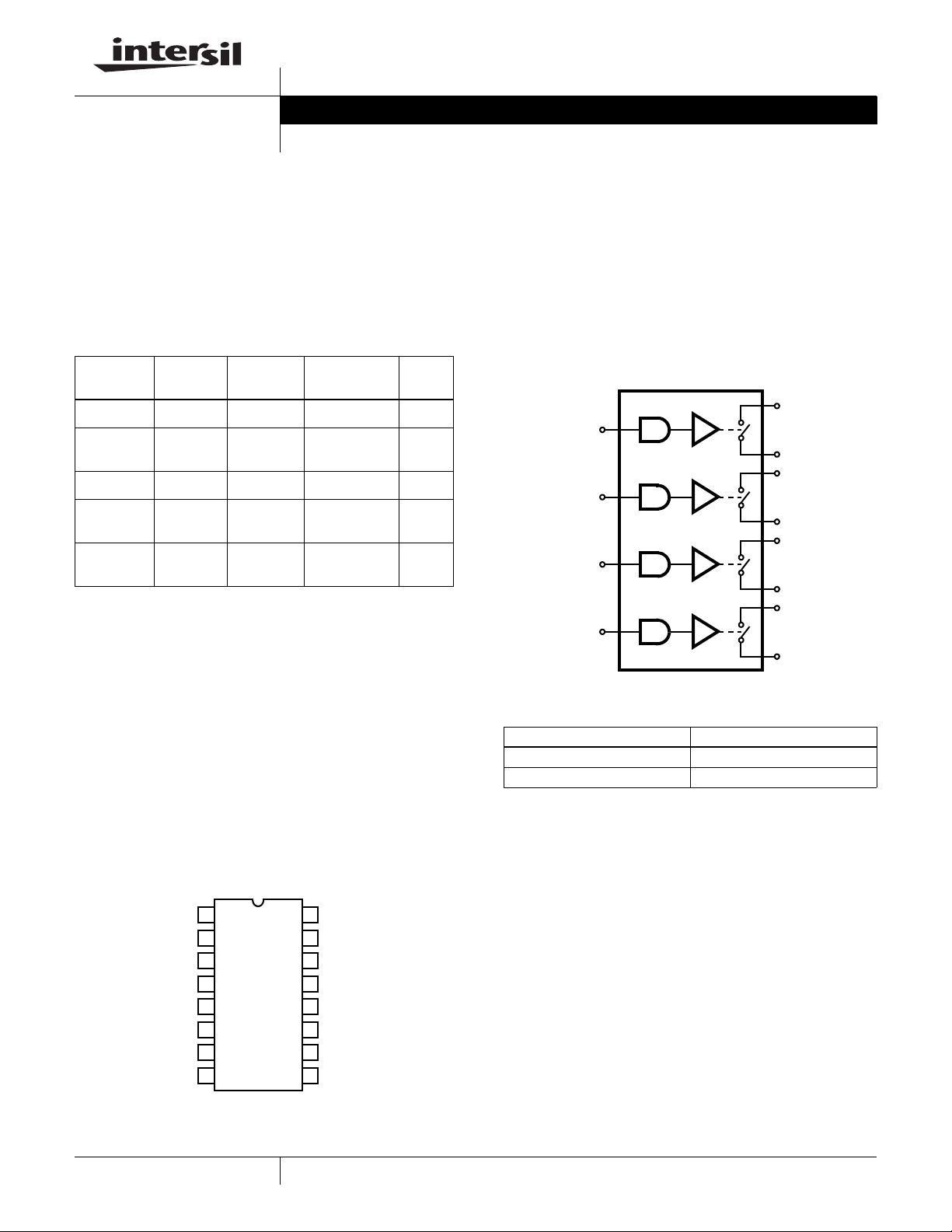
The DG211 is a low cost, CMOS monolithic, Quad SPST
analog switch. It can be used in general purpose switching
applications for communications, instrumentation, process
control and computer peripheral equipment and provides
true bi-directional performance in the ON condition and
blocks signals to 30V
in the OFF condition.
P-P
Ordering Information
PART
NUMBER
DG211CJ DG211CJ 0 to +70 16 Ld PDIP E16.3
DG211CJZ
(Note)
DG211CY** DG211CY 0 to +70 16 Ld SOIC M16.15
DG211CYZ**
(Note)
DG211CVZ**
(Note)
*Pb-free PDIPs can be used for through hole wave solder processing
only. They are not intended for use in Reflow solder processing
applications.
**Add “-T” suffix for tape and reel. Please refer to TB347 for details
on reel specifications.
NOTE: These Intersil Pb-free plastic packaged products employ
special Pb-free material sets; molding compounds/die attach
materials and 100% matte tin plate PLUS ANNEAL - e3 termination
finish, which is RoHS compliant and compatible with both SnPb and
Pb-free soldering operations. Intersil Pb-free products are MSL
classified at Pb-free peak reflow temperatures that meet or exceed
the Pb-free requirements of IPC/JEDEC J STD-020.
PART
MARKING
TEMP.
RANGE (°C) PACKAGE
DG211CJZ 0 to +70 16 Ld PDIP*
(Pb-free)
DG211CYZ 0 to +70 16 Ld SOIC
(Pb-free)
DG211 CVZ 0 to +70 16 Ld TSSOP
(Pb-free)
PKG.
DWG. #
E16.3
M16.15
M16.173
Pinout
DG211
(16 LD PDIP, SOIC, TSSOP)
TOP VIEW
Features
• Switches ±15V Analog Signals
• TTL Compatibility
• Logic Inputs Accept Negative Voltages
(Max). . . . . . . . . . . . . . . . . . . . . . . . . . . . . . . . . 175Ω
•r
ON
• Pb-Free Available (RoHS Compliant)
Functional Block Diagram
DG211
S
IN
1
D
S
IN
2
D
S
IN
3
D
S
IN
4
D
TRUTH TABLE
LOGIC DG211
0ON
1OFF
Logic “0” ≤0.8V, Logic “1” ≥ 2.4V
FN3118.5
1
1
2
2
3
3
4
4
IN
D
S
GND
S
D
IN
1
1
2
1
3
1
4
V-
5
6
4
7
4
8
4
16
IN
2
15
D
2
14
S
2
13
V+ (SUBSTRATE)
12
V
(+5V)
L
11
S
3
10
D
3
9
IN
3
1
CAUTION: These devices are sensitive to electrostatic discharge; follow proper IC Handling Procedures.
1-888-INTERSIL or 1-888-468-3774
| Intersil (and design) is a registered trademark of Intersil Americas Inc.
Copyright Intersil Americas Inc. 2001, 2005, 2007. All Rights Reserved
All other trademarks mentioned are the property of their respective owners.
Page 2
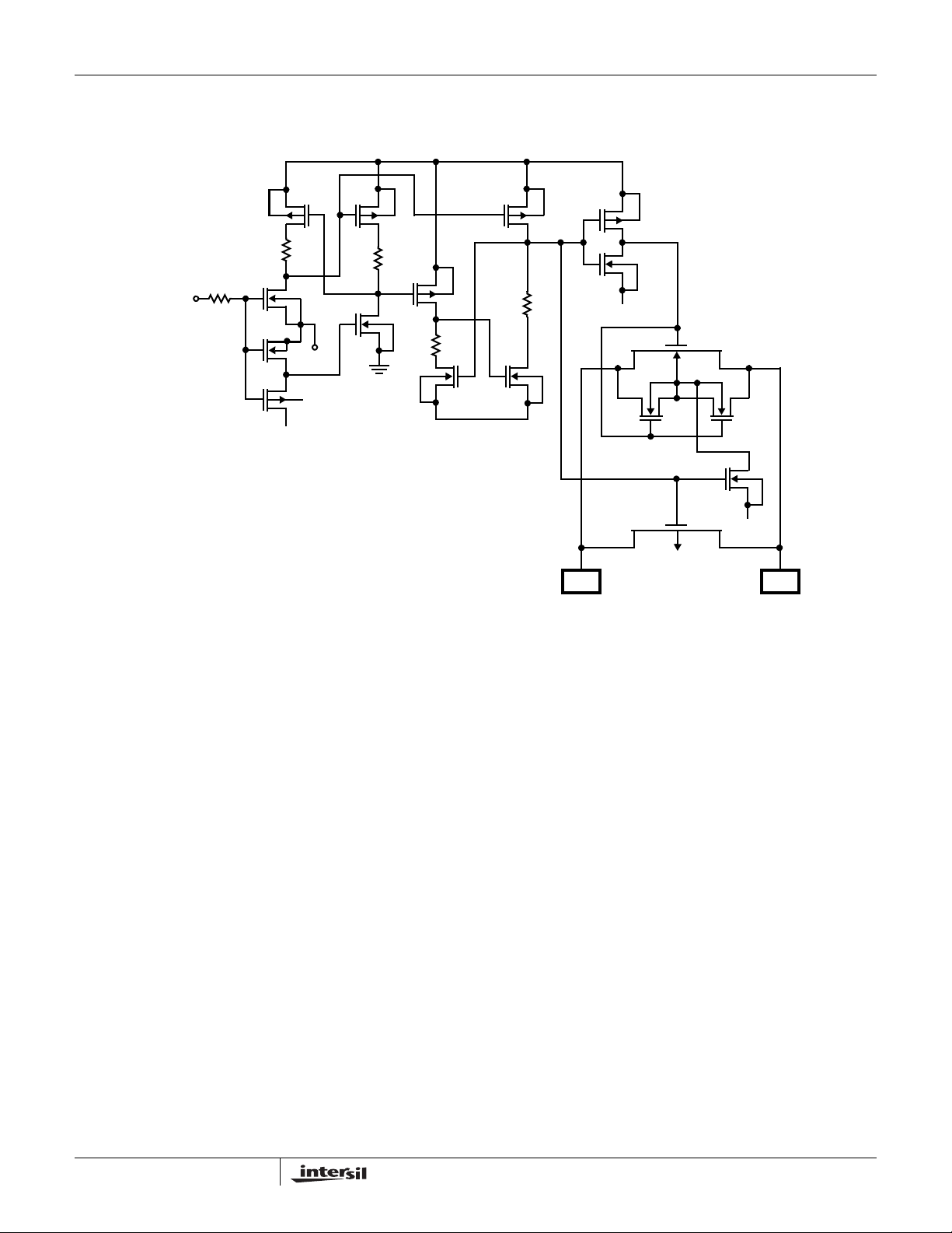
Schematic Diagram
TTL IN
DG211
DG211 (1/4 AS SHOWN)
-15V
GND
+15V
+5V
V
-15V
L
V-
-15V
+15V
OUTIN
2
FN3118.5
November 19, 2007
Page 3
DG211
Absolute Maximum Ratings Thermal Information
V+ to V- . . . . . . . . . . . . . . . . . . . . . . . . . . . . . . . . . . . . . . . . . . . 44V
V
to Ground . . . . . . . . . . . . . . . . . . . . . . . . . . . . . . . . . . . V- to V+
IN
V
to Ground . . . . . . . . . . . . . . . . . . . . . . . . . . . . . . . . -0.3V to 25V
L
V
or VD to V+. . . . . . . . . . . . . . . . . . . . . . . . . . . . . . . . . 0V to -36V
S
V
or VD to V- . . . . . . . . . . . . . . . . . . . . . . . . . . . . . . . . . 0V to 36V
S
V+ to Ground . . . . . . . . . . . . . . . . . . . . . . . . . . . . . . . . . . . . . . . 25V
V- to Ground. . . . . . . . . . . . . . . . . . . . . . . . . . . . . . . . . . . . . . . -25V
Current, any Terminal Except S or D . . . . . . . . . . . . . . . . . . . . 30mA
Continuous Current, S or D . . . . . . . . . . . . . . . . . . . . . . . . . . . 20mA
Peak Current, S or D (Pulsed 1ms, 10% Duty Cycle Max) . . . . . 70mA
Operating Conditions
Temperature Range. . . . . . . . . . . . . . . . . . . . . . . . . . . 0°C to +70°C
CAUTION: Do not operate at or near the maximum ratings listed for extended periods of time. Exposure to such conditions may adversely impact product reliability and
result in failures not covered by warranty.
NOTE:
is measured with the component mounted on an evaluation PC board in free air.
1. θ
JA
Thermal Resistance (Typical, Note 1)
θ
(°C/W)
JA
PDIP Package* . . . . . . . . . . . . . . . . . . . . . . . . . . . . 100
SOIC Package . . . . . . . . . . . . . . . . . . . . . . . . . . . . . 120
TSSOP Package . . . . . . . . . . . . . . . . . . . . . . . . . . . 150
Maximum Junction Temperature . . . . . . . . . . . . . . . . . . . . . .+150°C
Maximum Storage Temperature Range. . . . . . . . . .-65°C to +150°C
Pb-free reflow profile . . . . . . . . . . . . . . . . . . . . . . . . . .see link below
http://www.intersil.com/pbfree/Pb-FreeReflow.asp
*Pb-free PDIPs can be used for through hole wave solder
processing only. They are not intended for use in Reflow solder
processing applications.
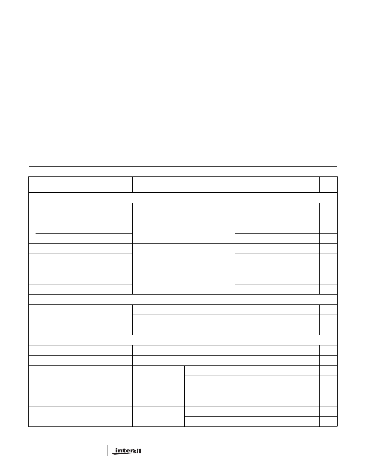
Electrical Specifications V+ = +15V, V- = -15V, V
PARAMETER TEST CONDITIONS
= +5V, GND, TA = +25°C
L
MIN
(Notes 2, 6)
TYP
(Note 3)
MAX
(Notes 2, 6) UNITS
DYNAMIC CHARACTERISTICS
Turn-ON Time, t
ON
Turn-OFF Time
t
OFF1
t
OFF2
OFF Isolation, OIRR (Note 5) V
Crosstalk (Channel-to-Channel), CCRR - -90 - dB
Source OFF-Capacitance, C
Drain OFF-Capacitance, C
Channel ON-Capacitance, C
S(OFF)
D(OFF)
D(ON) + CS(ON)
See Figure 1
V
= 10V, RL = 1kΩ, CL = 35pF
S
- 460 - ns
- 360 - ns
- 450 - ns
= 5V, RL = 1kΩ, CL = 15pF, VS = 1V
IN
RMS
,
-70-dB
f = 100kHz
VD = VS = 0V, VIN = 5V, f = 1MHz - 5 - pF
-5-pF
-16-pF
DIGITAL INPUT CHARACTERISTICS
Input Current with Voltage High, I
Input Current with Voltage Low, I
IH
IL
VIN = 2.4V -1.0 -0.0004 - µA
V
= 15V - 0.003 1.0 µA
IN
VIN = 0V -1.0 -0.0004 - µA
ANALOG SWITCH CHARACTERISTICS
Analog Signal Range, V
ANALOG
Drain-Source ON-Resistance, r
Source OFF Leakage Current, I
Drain OFF Leakage Current, I
Drain ON Leakage Current, I
(Note 4)
D(ON)
DS(ON)
S(OFF)
D(OFF)
VD = ±10V, IS = 1mA, VIN = 0.8V - 150 175 Ω
VIN = 2.4V VS = 14V, VD = -14V - 0.01 5.0 nA
V
= -14V, VD = 14V -5.0 -0.02 - nA
S
VS = -14V, VD = 14V - 0.01 5.0 nA
V
= 14V, VD = -14V -5.0 -0.02 - nA
S
= 0.8V VS = VD = 14V - 0.1 5.0 nA
V
IN
V
= VD = -14V -5.0 -0.15 - nA
S
-15 - 15 V
3
FN3118.5
November 19, 2007
Page 4
DG211
Electrical Specifications V+ = +15V, V- = -15V, V
PARAMETER TEST CONDITIONS
= +5V, GND, TA = +25°C (Continued)
L
MIN
(Notes 2, 6)
TYP
(Note 3)
MAX
(Notes 2, 6) UNITS
POWER SUPPLY CHARACTERISTICS
Positive Supply Current, I+ V
= 0V or 2.4V - 0.1 10 µA
IN
Negative Supply Current, I- -0.110µA
Logic Supply Current, I
L
-0.110µA
NOTES:
2. The algebraic convention whereby the most negative value is a minimum, and the most positive is a maximum, is used in this data sheet.
3. For design reference only, not 100% tested.
4. I
5. .
is leakage from driver into ON switch.
D(ON)
OFF Isolation 20
V
S
------- -
log Input to OFF switch, VDoutput== =
,V
S
V
D
6. Parts are 100% tested at +25°C. Over-temperature limits established by characterization and are not production tested.
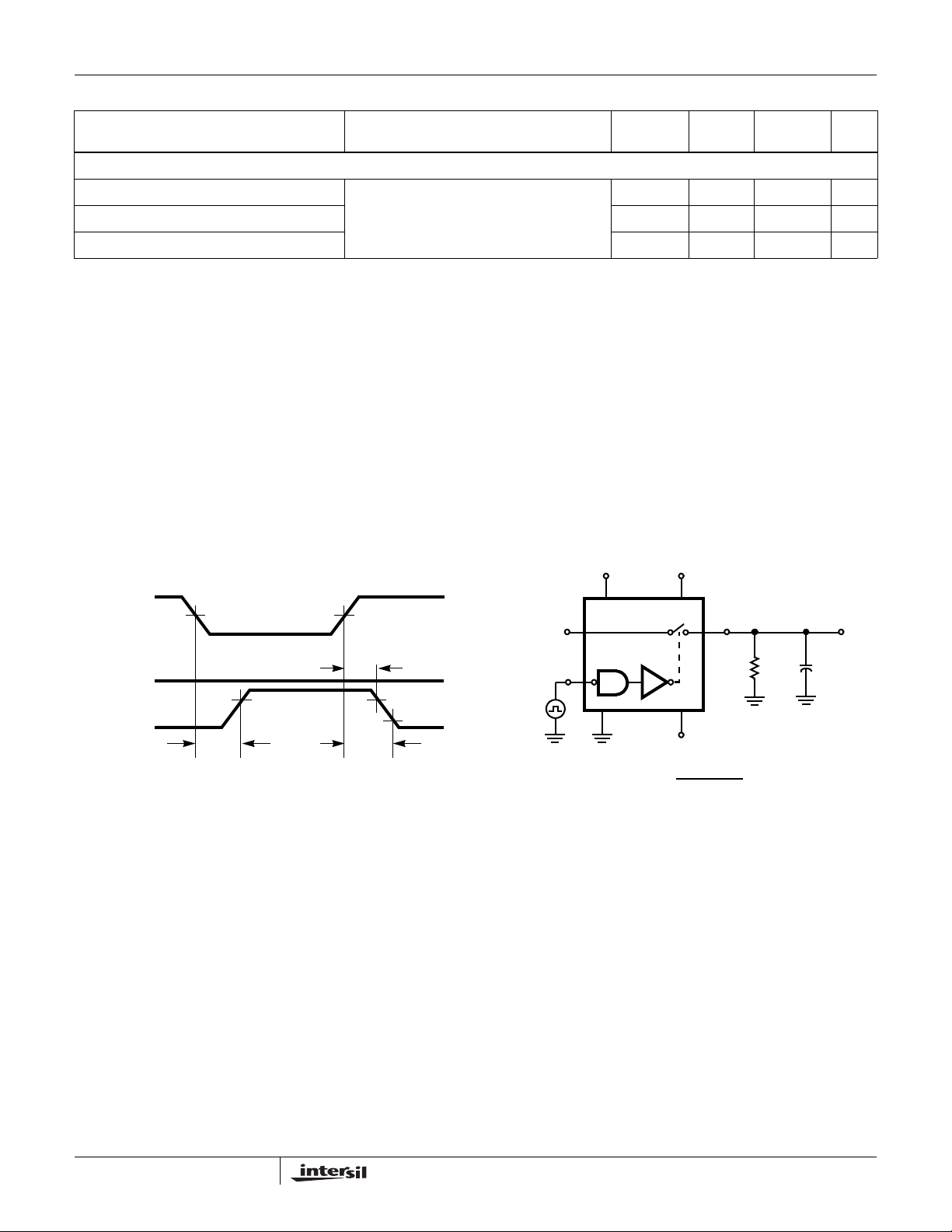
Test Circuits and Waveforms
Switch output waveform shown for VS = constant with logic
input waveform as shown. Note the V
switching time test circuit. V
is the steady state output with
O
switch on. Feedthrough via gate capacitance may result in
spikes at leading and trailing edge of output waveform.
may be + or - as per
S
LOGIC†
tr < 20ns
< 20ns
t
f
V
SWITCH
)
1
S
)
O
0V
50%
t
ON
90%
t
OFF1
t
OFF2
INPUT (IN
SWITCH
INPUT
OUTPUT (V
† Logic shown for DG211.
FIGURE 1. SWITCHING TIME MEASUREMENT POINTS
90%
10%
SWITCH
INPUT
V
= 10V
S
LOGIC
INPUT
5V
V
L
S
1
IN
1
GND
15V
V+
D
V-
-15V
R
V
= V
O
S
RL + r
L
DS(ON)
FIGURE 2. SWITCHING TIME TEST CIRCUIT
1
R
L
1kΩ
(REPEAT TEST FOR
IN
, IN3 AND IN4)
2
SWITCH
OUTPUT
C
L
35pF
V
O
4
FN3118.5
November 19, 2007
Page 5
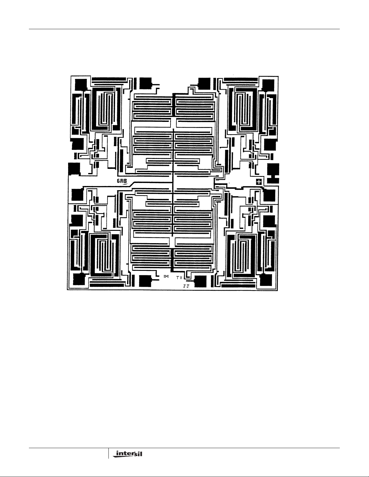
Metallization Mask Layout
DG211
DG211
PIN 2
D1
PIN 3
S1
PIN 4
PIN 5
GND
PIN 6
S4
PIN 1
IN1
V-
PIN 16
IN2
PIN 15
D2
PIN 14
S2
PIN 13
V+ (SUBSTRATE)
PIN 12
VL
PIN 11
S3
PIN 7
D4
PIN 8
IN 4
5
PIN 9
IN 3
PIN 10
D3
FN3118.5
November 19, 2007
Page 6
DG211
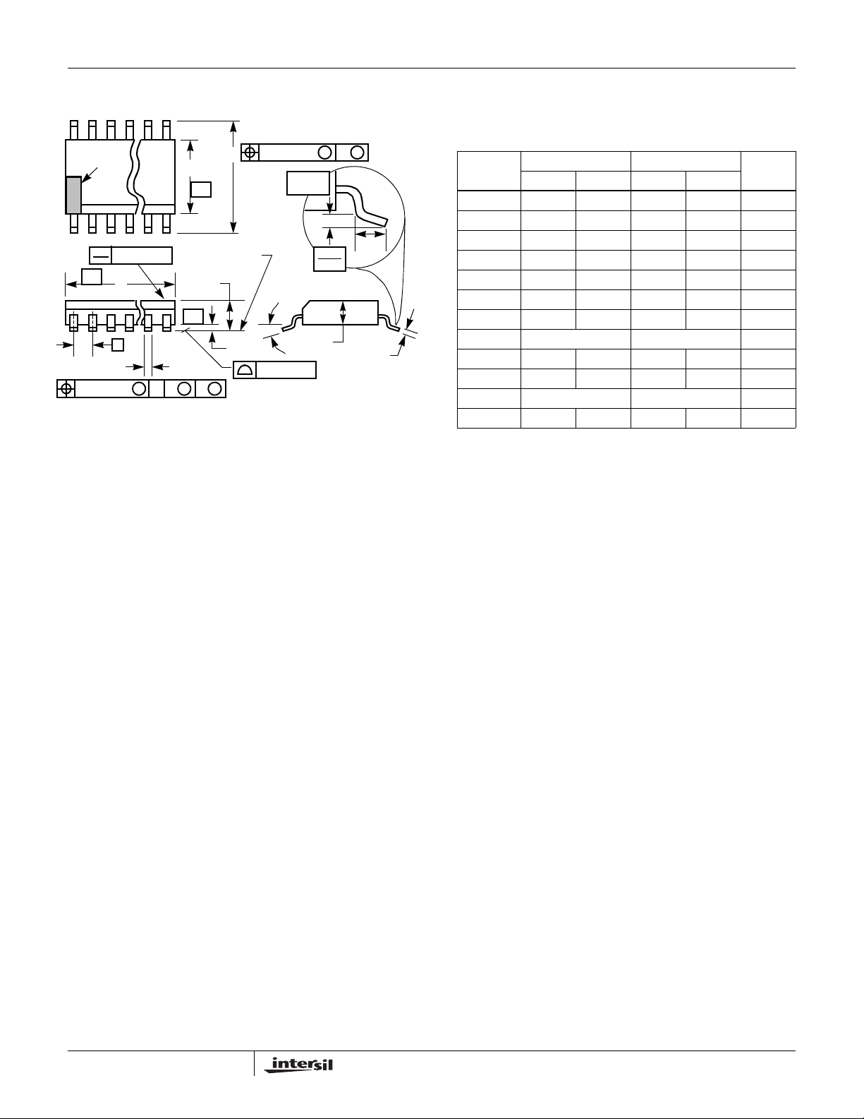
Thin Shrink Small Outline Plastic Packages (TSSOP)
N
INDEX
AREA
123
-A-
0.05(0.002)
D
SEATING PLANE
e
b
0.10(0.004) C AM BS
E1
-B-
A
-C-
M
0.25(0.010) BM M
E
α
A1
0.10(0.004)
GAUGE
PLANE
0.25
0.010
A2
NOTES:
1. These package dimensions are within allowable dimensions of
JEDEC MO-153-AB, Issue E.
2. Dimensioning and tolerancing per ANSI Y14.5M-1982.
3. Dimension “D” does not include mold flash, protrusions or gate
burrs. Mold flash, protrusion and gate burrs shall not exceed
0.15mm (0.006 inch) per side.
4. Dimension “E1” does not include interlead flash or protrusions.
Interlead flash and protrusions shall not exceed 0.15mm (0.006
inch) per side.
5. The chamfer on the body is optional. If it is not present, a visual
index feature must be located within the crosshatched area.
6. “L” is the length of terminal for soldering to a substrate.
7. “N” is the number of terminal positions.
8. Terminal numbers are shown for reference only.
9. Dimension “b” does not include dambar protrusion. Allowable
dambar protrusion shall be 0.08mm (0.003 inch) total in excess
of “b” dimension at maximum material condition. Minimum space
between protrusion and adjacent lead is 0.07mm (0.0027 inch).
10. Controlling dimension: MILLIMETER. Converted inch dimensions are not necessarily exact. (Angles in degrees)
M16.173
16 LEAD THIN SHRINK SMALL OUTLINE PLASTIC PACKAGE
INCHES MILLIMETERS
SYMBOL
A - 0.043 - 1.10 -
A1 0.002 0.006 0.05 0.15 -
L
A2 0.033 0.037 0.85 0.95 -
b 0.0075 0.012 0.19 0.30 9
c 0.0035 0.008 0.09 0.20 -
D 0.193 0.201 4.90 5.10 3
E1 0.169 0.177 4.30 4.50 4
e 0.026 BSC 0.65 BSC -
c
E 0.246 0.256 6.25 6.50 -
L 0.020 0.028 0.50 0.70 6
N16 167
o
α
0
o
8
o
0
8
o
Rev. 1 2/02
NOTESMIN MAX MIN MAX
-
6
FN3118.5
November 19, 2007
Page 7
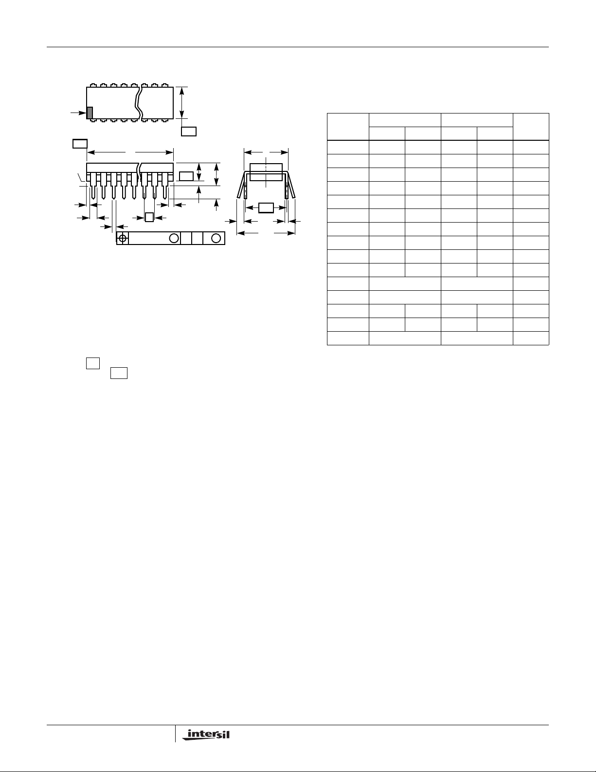
Dual-In-Line Plastic Packages (PDIP)
DG211
N
D1
-C-
E1
-B-
A1
A2
E
A
L
e
C
C
L
e
A
C
e
B
INDEX
AREA
BASE
PLANE
SEATING
PLANE
D1
B1
12 3 N/2
-AD
e
B
0.010 (0.25) C AM BS
NOTES:
1. Controlling Dimensions: INCH. In case of conflict between English and
Metric dimensions, the inch dimensions control.
2. Dimensioning and tolerancing per ANSI Y14.5M-1982.
3. Symbols are defined in the “MO Series Symbol List” in Section 2.2 of
Publication No. 95.
4. Dimensions A, A1 and L are measured with the package seated in JEDEC seating plane gauge GS-3.
5. D, D1, and E1 dimensions do not include mold flash or protrusions.
Mold flash or protrusions shall not exceed 0.010 inch (0.25mm).
6. E and are measured with the leads constrained to be perpendic-
7. e
e
A
ular to datum .
and eC are measured at the lead tips with the leads unconstrained.
B
e
must be zero or greater.
C
-C-
8. B1 maximum dimensions do not include dambar protrusions. Dambar
protrusions shall not exceed 0.010 inch (0.25mm).
9. N is the maximum number of terminal positions.
10. Corner leads (1, N, N/2 and N/2 + 1) for E8.3, E16.3, E18.3, E28.3,
E42.6 will have a B1 dimension of 0.030 - 0.045 inch (0.76 - 1.14mm).
E16.3 (JEDEC MS-001-BB ISSUE D)
16 LEAD DUAL-IN-LINE PLASTIC PACKAGE
INCHES MILLIMETERS
SYMBOL
A-0.210 - 5.33 4
A1 0.015 - 0.39 -4
A2 0.115 0.195 2.93 4.95 -
B 0.014 0.022 0.356 0.558 B1 0.045 0.070 1.15 1.77 8, 10
C 0.008 0.014 0.204 0.355 -
D 0.735 0.775 18.66 19.68 5
D1 0.005 - 0.13 -5
E 0.300 0.325 7.62 8.25 6
E1 0.240 0.280 6.10 7.11 5
e 0.100 BSC 2.54 BSC e
A
e
B
0.300 BSC 7.62 BSC 6
- 0.430 - 10.92 7
L 0.115 0.150 2.93 3.81 4
N16 169
NOTESMIN MAX MIN MAX
Rev. 0 12/93
7
FN3118.5
November 19, 2007
Page 8
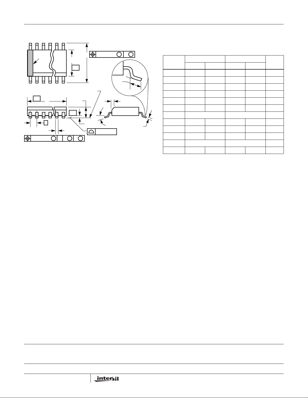
Small Outline Plastic Packages (SOIC)
DG211
N
INDEX
AREA
123
-A-
E
-B-
SEATING PLANE
D
A
-C-
0.25(0.010) BM M
H
L
h x 45°
α
e
B
0.25(0.010) C AM BS
M
NOTES:
1. Symbols are defined in the “MO Series Symbol List” in Section 2.2 of
Publication Number 95.
2. Dimensioning and tolerancing per ANSI Y14.5M-1982.
3. Dimension “D” does not include mold flash, protrusions or gate burrs.
Mold flash, protrusion and gate burrs shall not exceed 0.15mm (0.006
inch) per side.
4. Dimension “E” does not include interlead flash or protrusions. Interlead
flash and protrusions shall not exceed 0.25mm (0.010 inch) per side.
5. The chamfer on the body is optional. If it is not present, a visual index
feature must be located within the crosshatched area.
6. “L” is the length of terminal for soldering to a substrate.
7. “N” is the number of terminal positions.
8. Terminal numbers are shown for reference only.
9. The lead width “B”, as measured 0.36mm (0.014 inch) or greater above
the seating plane, shall not exceed a maximum value of 0.61mm
(0.024 inch).
10. Controlling dimension: MILLIMETER. Converted inch dimensions are
not necessarily exact.
A1
C
0.10(0.004)
M16.15 (JEDEC MS-012-AC ISSUE C)
16 LEAD NARROW BODY SMALL OUTLINE PLASTIC PACKAGE
INCHES MILLIMETERS
SYMBOL
A 0.0532 0.0688 1.35 1.75 -
A1 0.0040 0.0098 0.10 0.2 5 -
B 0.013 0.020 0.33 0.51 9
C 0.0075 0.0098 0.19 0.25 D 0.3859 0.3937 9.80 10.00 3
E 0.1497 0.1574 3.80 4.00 4
e 0.050 BSC 1.27 BSC H 0.2284 0.2440 5.80 6.20 h 0.0099 0.0196 0.25 0.50 5
L 0.016 0.050 0.40 1.27 6
N16 167
α
0° 8° 0° 8° -
NOTESMIN MAX MIN MAX
Rev. 1 6/05
All Intersil U.S. products are manufactured, assembled and tested utilizing ISO9000 quality systems.
Intersil Corporation’s quality certifications can be viewed at www.intersil.com/design/quality
Intersil products are sold by description only. Intersil Corporation reserves the right to make changes in circuit design, software and/or specifications at any time without
notice. Accordingly, the reader is cautioned to verify that data sheets are current before placing orders. Information furnished by Intersil is believed to be accurate and
reliable. However, no responsibility is assumed by Intersil or its subsidiaries for its use; nor for any infringements of patents or other rights of third parties which may result
from its use. No license is granted by implicat ion or oth erwise u nde r any p a tent or p at ent r ights of Intersil or its subsidiaries.
For information regarding Intersil Corporation and its products, see www.intersil.com
8
FN3118.5
November 19, 2007
 Loading...