

®
www.BDTIC.com/Intersil
82C89
Data Sheet February 27, 2006
CMOS Bus Arbiter
The Intersil 82C89 Bus Arbiter is manufactured using a selfaligned silicon gate CMOS process (Scaled SAJI IV). This
circuit, along with the 82C88 bus controller, provides full bus
arbitration and control for multi-processor systems. The 82C89
is typically used in medium to large 80C86 or 80C88 systems
where access to the bus by several processors must be
coordinated. The 82C89 also provides high output current and
capacitive drive to eliminate the need for additional bus
buffering.
Static CMOS circuit design insures low operating power. The
advanced Intersil SAJI CMOS process results in
performance equal to or greater than existing equivalent
products at a significant power savings.
Ordering Information
PAR T
NUMBER
CP82C89 CP82C89 0 to +70 20 Ld PDIP E20.3
CP82C89Z*
(Note)
MD82C89/B MD82C89/B -55 to +125 20 Ld CERDIP F20.3
NOTE: Intersil Pb-free plus anneal products employ special Pb-free
material sets; molding compounds/die attach materials and 100%
matte tin plate termination finish, which are RoHS compliant and
compatible with both SnPb and Pb-free soldering operations. Intersil
Pb-free products are MSL classified at Pb-free peak reflow
temperatures that meet or exceed the Pb-free requirements of
IPC/JEDEC J STD-020.
*Pb-free PDIPs can be used for through hole wave solder processing
only. They are not intended for use in Reflow solder processing
applications.
PART
MARKING
CP82C89Z 0 to +70 20 Ld PDIP
TEMP.
RANGE (°C) PACKAGE
(Pb-free)
PKG.
DWG. #
E20.3
FN2980.2
Features
• Pin Compatible with Bipolar 8289
• Performance Compatible with:
- 80C86/80C88 . . . . . . . . . . . . . . . . . . . . . . . . . (5/8MHz)
• Provides Multi-Master System Bus Control and
Arbitration
• Provides Simple Interface with 82C88/8288 Bus
Controller
• Synchronizes 80C86/8086, 80C88/8088 Processors with
Multi-Master Bus
• Bipolar Drive Capability
• Four Operating Modes for Flexible System Configuration
• Low Power Operation
- ICCSB. . . . . . . . . . . . . . . . . . . . . . . . . . . . . .10µA (Max)
- ICCOP . . . . . . . . . . . . . . . . . . . . . . . . . 1mA/MHz (Max)
• Operating Temperature Ranges
- C82C89 . . . . . . . . . . . . . . . . . . . . . . . . . . 0°C to +70°C
- M82C89 . . . . . . . . . . . . . . . . . . . . . . . .-55°C to +125°C
• Pb-Free Plus Anneal Available (RoHS Compliant)
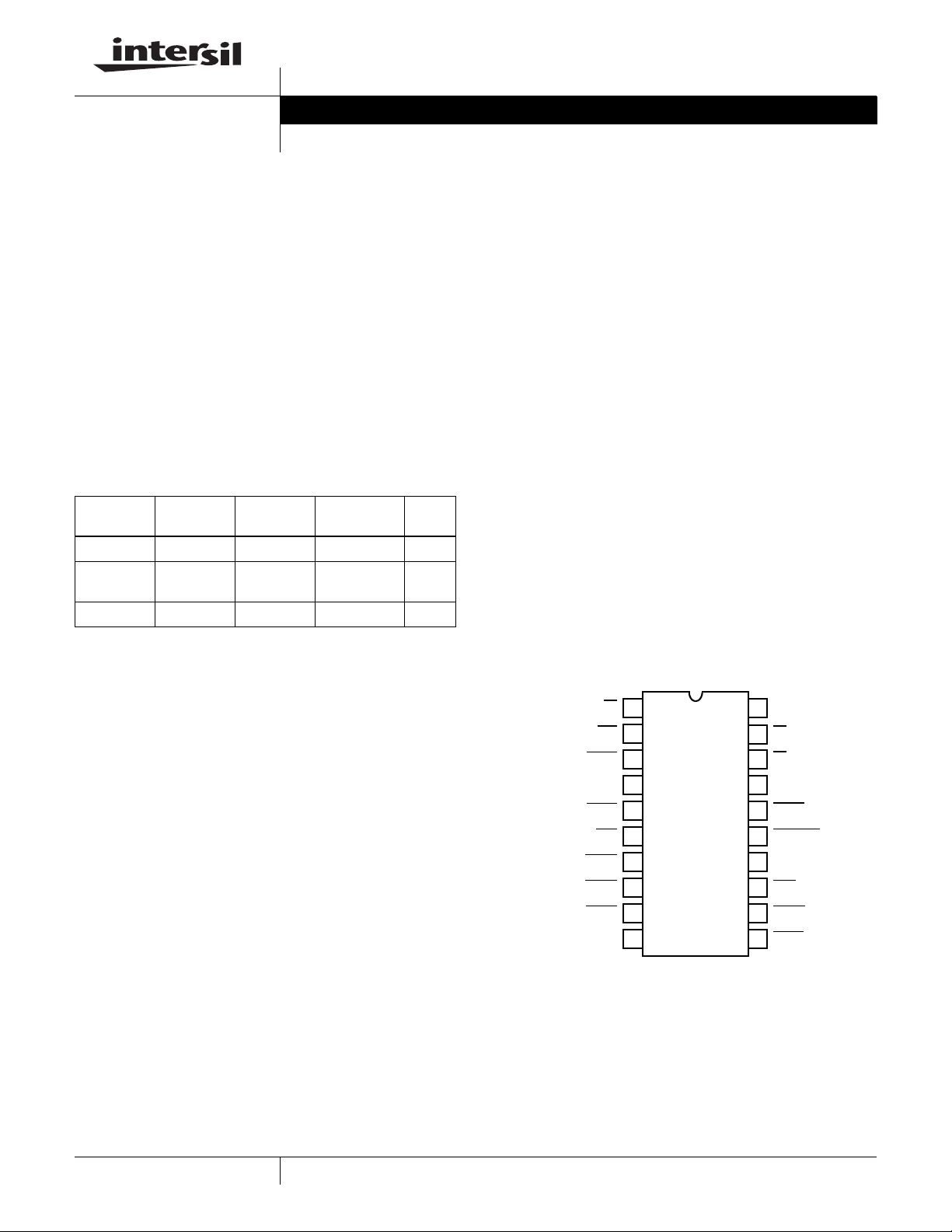
Pinout
82C89 (PDIP, CERDIP)
TOP VIEW
S2
IOB
SYSB/RESB
RESB
BCLK
INIT
BREQ
BPRO
BPRN
GND
1
2
3
4
5
6
7
8
9
10
20
19
18
17
16
15
14
13
12
11
V
CC
S1
S0
CLK
LOCK
CRQLCK
ANYRQST
AEN
CBRQ
BUSY
1
CAUTION: These devices are sensitive to electrostatic discharge; follow proper IC Handling Procedures.
1-888-INTERSIL or 1-888-468-3774
| Intersil (and design) is a registered trademark of Intersil Americas Inc.
All other trademarks mentioned are the property of their respective owners.
Copyright Intersil Americas Inc. 1997, 2006. All Rights Reserved
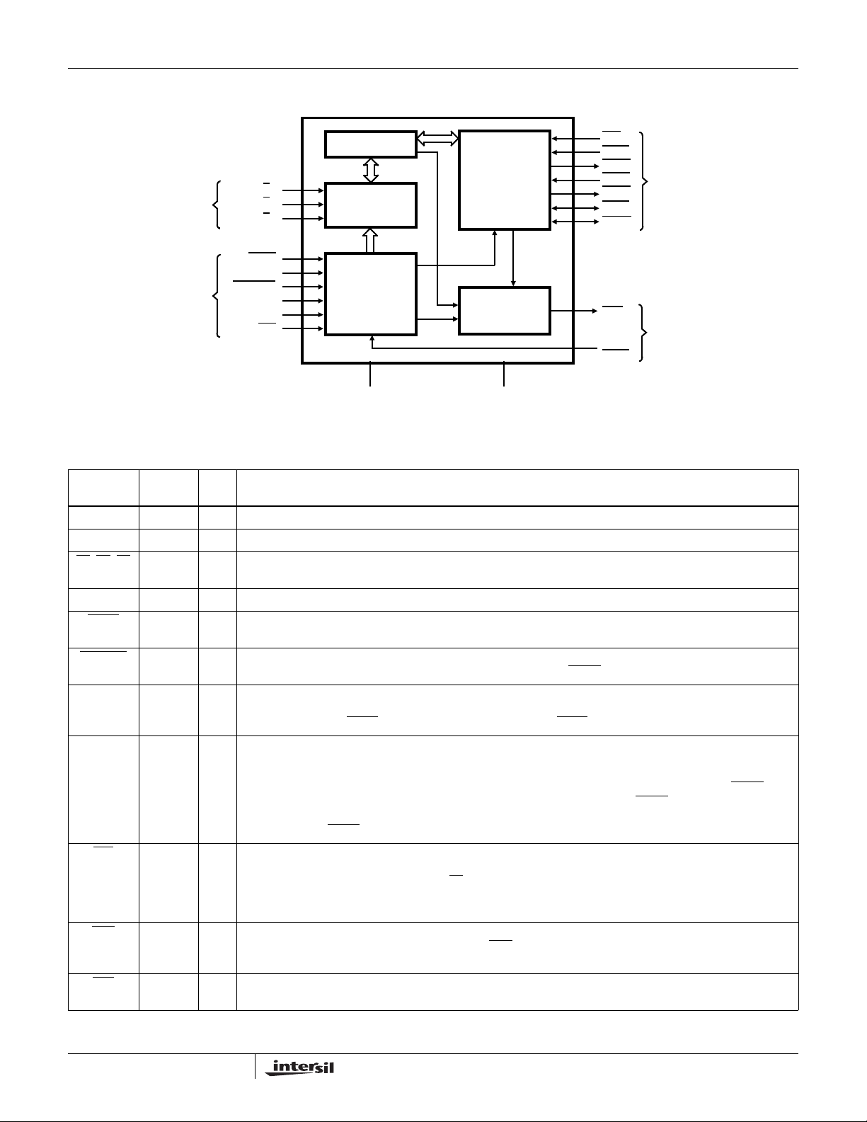
Functional Diagram
www.BDTIC.com/Intersil
82C89
INIT
BCLK
BREQ
BPRN
BPRO
BUSY
CBRQ
AEN
SYSB/
RESB
MULTIBUS™
COMMAND
SIGNALS
SYSTEM
SIGNALS
MULTIBUS™ is an Intel Corp. trademark.
80C86/
80C88
STATUS
CONTROL/
STRAPPING
OPTIONS
LOCK
CLK
CRQLCK
RESB
ANYRQST
IOB
ARBITRATION
MULTIBUS
S
2
S
1
S
0
STATUS
DECODER
CONTROL
+5V GND
INTERFACE
LOCAL
BUS
INTERFACE
Pin Description
PIN
SYMBOL NUMBER TYPE DESCRIPTION
V
CC
GND 10 GROUND.
, S1, S2 1, 18-19 I STATUS INPUT PINS: The status input pins from an 80C86, 80C88 or 8089 processor. The 82C89 decodes
S0
CLK 17 I CLOCK: From the 82C84A or 82C85 clock chip and serves to establish when bus arbiter actions are initiated.
LOCK
CRQLCK
RESB 4 I RESIDENT BUS: A strapping option to configure the arbiter to operate in systems having both a multi-master
ANYRQST 14 I ANY REQUEST: A strapping option which permits the multi-master system bus to be surrendered to a lower
IOB
AEN
INIT
20 VCC: The +5V Power supply pin. A 0.1µF capacitor between pins 10 and 20 is recommended for decoupling.
these pins to initiate bus request and surrender actions. (See Table 1).
16 I LOCK: A processor generated signal which when activated (low) prevents the arbiter from surrendering the multi-
master system bus to any other bus arbiter, regardless of its priority.
15 I COMMON REQUEST LOCK: An active low signal which prevents the arbiter from surrendering the multi-master
system bus to any other bus arbiter requesting the bus through the CBRQ
input pin.
system bus and a Resident Bus. Strapped high, the multi-master system bus is requested or surrendered as a
function of the SYSB/RESB
input pin. Strapped low, the SYSB/RESB input is ignored.
priority arbiter as if it were an arbiter of higher priority (i.e., when a lower priority arbiter requests the use of the
multi-master system bus, the bus is surrendered as soon as it is possible). When ANYRQST is strapped low, the
bus is surrendered according to Table A in Design Information. If ANYRQST is strapped high and CBRQ
activated, the bus is surrendered at the end of the present bus cycle. Strapping CBRQ
low and ANYRQST high
forces the 82C89 arbiter to surrender the multi-master system bus after each transfer cycle. Note that when
surrender occurs BREQ
is driven false (high).
2 I IO BUS: A strapping option which configures the 82C89 Arbiter to operate in systems having both an IO Bus
(Peripheral Bus) and a multi-master system bus. The arbiter requests and surrenders the use of the multi-master
system bus as a function of the status line, S2
. The multi-master system bus is permitted to be surrendered while
the processor is performing IO commands and is requested whenever the processor performs a memory
command. Interrupt cycles are assumed as coming from the peripheral bus and are treated as an IO command.
13 O ADDRESS ENABLE: The output of the 82C89 Arbiter to the processor’s address latches, to the 82C88 Bus
Controller and 82C84A or 82C85 Clock Generator. AEN
serves to instruct the Bus Controller and address latches
when to three-state their output drivers.
6 I INITIALIZE: An active low multi-master system bus input signal used to reset all the bus arbiters on the multi-
master system bus. After initialization, no arbiters have the use of the multi-master system bus.
is
2
FN2980.2
February 27, 2006
82C89
www.BDTIC.com/Intersil
Pin Description (Continued)
PIN
SYMBOL NUMBER TYPE DESCRIPTION
SYSB/RESB 3 I SYSTEM BUS/RESIDENT BUS: An input signal when the arbiter is configured in the System/Resident Mode
is strapped high) which determines when the multi-master system bus is requested and multi-master
(RESB
system bus surrendering is permitted. The signal is intended to originate from a form of address-mapping
circuitry, such as a decoder or PROM attached to the resident address bus. Signal transitions and glitches are
permitted on this pin from θ1 of T4 to θ1 of T2 of the processor cycle. During the period from θ1 of T2 to θ1 of T4,
only clean transitions are permitted on this pin (no glitches). If a glitch occurs, the arbiter may capture or miss it,
and the multi-master system bus may be requested or surrendered, depending upon the state of the glitch. The
arbiter requests the multi-master system bus in the System/Resident Mode when the state of the SYSB/RESB
pin is high and permits the bus to be surrendered when this pin is low.
CBRQ
BCLK
BREQ
BPRN
BPRO
BUSY 11 I/O BUSY: An active low open-drain multi-master system bus interface signal used to instruct all the arbiters on the
12 I/O COMMON BUS REQUEST: An input signal which instructs the arbiter if there are any other arbiters of lower
priority requesting the use of the multi-master system bus.
The CBRQ
bus upon request are connected together.
The Bus Arbiter running the current transfer cycle will not itself pull the CBRQ
connected to the CDRQ
transfer cycle drops its BREQ
Strapping CBRQ
transfer cycle. See the pin definition of ANYRQST.
5 I BUS CLOCK: The multi-master system bus clock to which all multi-master system bus interface signals are
synchronized.
7 O BUS REQUEST: An active low output signal in the Parallel Priority Resolving Scheme which the arbiter activates
to request the use of the multi-master system bus.
9 I BUS PRIORITY IN: The active low signal returned to the arbiter to instruct it that it may acquire the multi-master
system bus on the next falling edge of BCLK
requesting arbiter presently on the bus. The loss of BPRN
priority arbiter.
8 O BUS PRIORITY OUT: An active low output signal used in the serial priority resolving scheme where BPRO is
daisy-chained to BPRN
bus when the multi-master system bus is available. When the multi-master system bus is available the highest
requesting arbiter (determined by BPRN
When the arbiter is done with the bus, it releases the BUSY
another arbiter to acquire the multi-master system bus.
pins (open-drain output) of all the 82C89 Bus Arbiters which surrender to the multi-master system
line low. Any other arbiter
line can request the multi-master system bus. The arbiter presently running the current
signal and surrenders the bus whenever the proper surrender conditions exist.
low and ANYRQST high allows the multi-master system bus to be surrendered after each
. BPRN active indicates to the arbiter that it is the highest priority
instructs the arbiter that it has lost priority to a higher
of the next lower priority arbiter.
) seizes the bus and pulls BUSY low to keep other arbiters off of the bus.
signal, permitting it to go high and thereby allowing
Functional Description
The 82C89 Bus Arbiter operates in conjunction with the
82C88 Bus Controller to interface 80C86, 80C88 processors
to a multi-master system bus (both the 80C86 and 80C88 are
configured in their max mode). The processor is unaware of
the arbiter’s existence and issues commands as though it
has exclusive use of the system bus. If the processor does
not have the use of the multi-master system bus, the arbiter
prevents the Bus Controller (82C88), the data transceivers
and the address latches from accessing the system bus (e.g.
all bus driver outputs are forced into the high impedance
state). Since the command sequence was not issued by the
82C88, the system bus will appear as “Not Ready” and the
processor will enter wait states. The processor will remain in
Wait until the Bus Arbiter acquires the use of the multi-master
system bus whereupon the arbiter will allow the bus controller,
the data transceivers, and the address latches to access the
system. Typically, once the command has been issued and a
data transfer has taken place, a transfer acknowledge (XACK)
is returned to the processor to indicate “READY” from the
3
accessed slave device. The processor then completes its
transfer cycle. Thus the arbiter serves to multiplex a processor
(or bus master) onto a multi-master system bus and avoid
contention problems between bus masters.
Arbitration Between Bus Masters
In general, higher priority masters obtain the bus when a
lower priority master completes its present transfer cycle.
Lower priority bus masters obtain the bus when a higher
priority master is not accessing the system bus. A strapping
option (ANYRQST) is provided to allow the arbiter to
surrender the bus to a lower priority master as though it were
a master of higher priority. If there are no other bus masters
requesting the bus, the arbiter maintains the bus so long as
its processor has not entered the HALT State. The arbiter will
not voluntarily surrender the system bus and has to be forced
off by another master’s bus request, the HALT State being the
only exception. Additional strapping options permit other
modes of operation wherein the multi-master system bus is
surrendered or requested under different sets of conditions.
FN2980.2
February 27, 2006
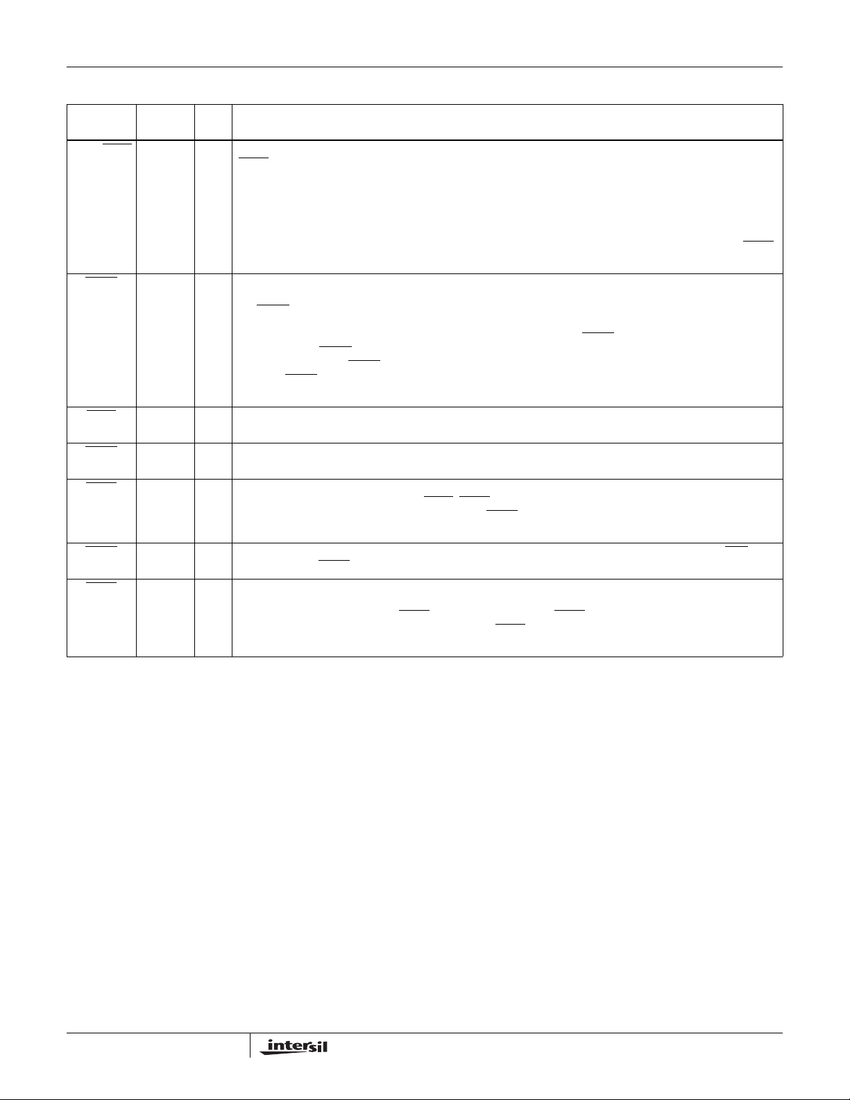
Priority Resolving Techniques
www.BDTIC.com/Intersil
Since there can be many bus masters on a multi-master
system bus, some means of resolving priority between bus
masters simultaneously requesting the bus must be
provided. The 82C89 Bus Arbiter provides several resolving
techniques. All the techniques are based on a priority
concept that at a given time one bus master will have priority
above all the rest. There are provisions for using parallel
priority resolving techniques, serial priority resolving
techniques, and rotating priority techniques.
Parallel Priority Resolving
The parallel priority resolving technique uses a separate bus
request line BREQ
system bus, see Figure 1. Each BREQ
priority encoder which generates the binary address of the
highest priority BREQ
is decoded by a decoder to select the corresponding BPRN
(Bus Priority In) line to be returned to the highest priority
requesting arbiter. The arbiter receiving priority (BPRN
then allows its associated bus master onto the multi-master
system bus as soon as it becomes available (i.e., the bus is
no longer busy). When one bus arbiter gains priority over
another arbiter it cannot immediately seize the bus, it must
wait until the present bus transaction is complete. Upon
completing its transaction the present bus occupant
recognizes that it no longer has priority and surrenders the
bus by releasing BUSY
signal line which goes to every bus arbiter on the system
bus. When BUSY
presently has bus priority (BPRN
and pulls BUSY
waveform timing diagram, Figure 2. Note that all multimaster
system bus transactions are synchronized to the bus clock
(BCLK
). This allows the parallel priority resolving circuitry or
any other priority resolving scheme employed to settle.
•••
•
BUSY
CBRQ
FIGURE 1. PARALLEL PRIORITY RESOLVING TECHNIQUE
for each arbiter on the multi-master
line enters into a
line which is active. The binary address
. BUSY is an active low “OR” tied
goes inactive (high), the arbiter which
true) then seizes the bus
low to keep other arbiters off of the bus. See
BREQ
BUS
ARBITER
1
BUS
ARBITER
2
BREQ
BUS
ARBITER
3
BUS
ARBITER
4
BREQ
BREQ
BPRN
BPRN
BPRN
BPRN
74HC148
PRIORITY
ENCODER
••
••
74HC138
3 TO 8
ENCODER
true)
••
••
82C89
BCLK
BREQ
BPRN
BUSY
FIGURE 2. HIGHER PRIORITY ARBITER OBTAINING THE
NOTES:
1. Higher priority bus arbiter releases BUSY
2. Higher priority bus arbiter then acquires the bus and pulls BUSY
down.
3. Lower priority bus arbiter releases BUSY
4. Higher priority bus arbiter then acquires the bus and pulls BUSY
down.
1
2
3
BUS FROM A LOWER PRIORITY ARBITER
4
.
.
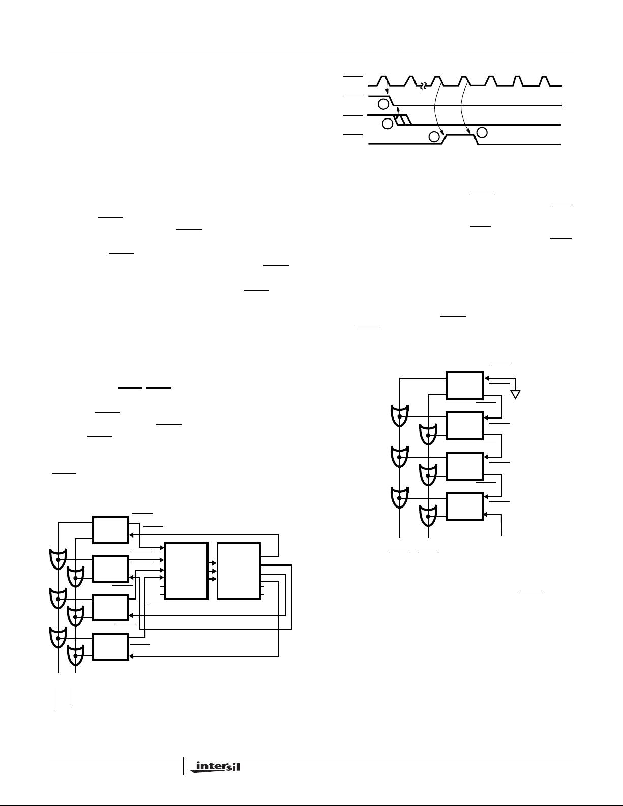
Serial Priority Resolving
The serial priority resolving technique eliminates the need
for the priority encoder-decoder arrangement by
daisychaining the bus arbiters together, connecting the
higher priority bus arbiter’s BPRO
to the BPRN
NOTE: The number of arbiters that may be daisy-chained together
in the serial priority resolving scheme is a function of BCLK
propagation delay from arbiter to arbiter. Normally, at 10MHz only 3
arbiters may be daisychained.
of the next lower priority. See Figure 3.
•
•
•
•
BUSYCBRQ
FIGURE 3. SERIAL PRIORITY RESOLVING
(Bus Priority Out) output
BUS
ARBITER
BUS
ARBITER
BUS
ARBITER
BUS
ARBITER
BPRN
BPRO
1
BPRN
BPRO
2
BPRN
BPRO
3
BPRN
BPRO
4
•
•
and the
Rotating Priority Resolving
The rotating priority resolving technique is similar to that of
the parallel priority resolving technique except that priority is
dynamically re-assigned. The priority encoder is replaced by
a more complex circuit which rotates priority between
requesting arbiters thus allowing each arbiter an equal
chance to use the multi-master system bus, over time.
4
FN2980.2
February 27, 2006

82C89
www.BDTIC.com/Intersil
Which Priority Resolving Technique To Use
There are advantages and disadvantages for each of the
techniques described above. The rotating priority resolving
technique requires substantial external logic to implement
while the serial technique uses no external logic but can
accommodate only a limited number of bus arbiters before the
daisy-chain propagation delay exceeds the multimaster’s
system bus clock (BCLK
technique is in general a good compromise between the other
two techniques. It allows for many arbiters to be present on
the bus while not requiring too much logic to implement.
). The parallel priority resolving
82C89 Modes Of Operation
There are two types of processors for which the 82C89 will
provide support: An Input/Output processor (i.e. an NMOS
8089 IOP) and the 80C86, 80C88. Consequently, there are
two basic operating modes in the 82C89 bus arbiter. One,
the IOB (I/O Peripheral Bus) mode, permits the processor
access to both an I/O Peripheral Bus and a multi-master
system bus. The second, the RESB (Resident Bus mode),
permits the processor to communicate over both a Resident
Bus and a multi-master system bus. An I/O Peripheral Bus is
a bus where all devices on that bus, including memory, are
treated as I/O devices and are addressed by I/O commands.
All memory commands are directed to another bus, the
multi-master system bus. A Resident Bus can issue both
memory and I/O commands, but it is a distinct and separate
bus from the multi-master system bus. The distinction is that
the Resident Bus has only one master, providing full
availability and being dedicated to that one master.
The IOB
into the IOB
configures it into the RESB mode. It might be noted at this
point that if both strapping options are strapped false, the
arbiter interfaces the processor to a multi-master system bus
only (see Figure 4). With both options strapped true, the
arbiter interfaces the processor to a multi-master system
bus, a Resident Bus, and an I/O Bus.
In the IOB
a host of peripherals over the Peripheral Bus. When the I/O
Processor needs to communicate with system memory, it
does so over the system memory bus. Figure 5 shows a
possible I/O Processor system configuration.
The 80C86 and 80C88 processors can communicate with a
Resident Bus and a multi-master system bus. Two bus
controllers and only one Bus Arbiter would be needed in
such a configuration as shown in Figure 6. In such a system
configuration the processor would have access to memory
and peripherals of both busses. Memory mapping
techniques are applied to select which bus is to be
accessed. The SYSB/RESB
instruct the arbiter as to whether or not the system bus is to
be accessed. The signal connected to SYSB/RESB
enables or disables commands from one of the bus
controllers. A summary of the modes that the 82C89 has,
along with its response to its status lines inputs, is shown in
Table 1.
strapping option configures the 82C89 Bus Arbiter
mode and the strapping option RESB
mode, the processor communicates and controls
input on the arbiter serves to
also
5
FN2980.2
February 27, 2006

AD0-AD15
www.BDTIC.com/Intersil
PROCESSOR
LOCAL BUS
READY
80C86
CPU
A16-A19
CLK
S0
S1
S2
X1
RDY2
GENERATOR
READY
CLK
X2
82C84A/85
CLOCK
AEN2
RDY1
AEN1
STATUS (S0
OE
V
CC
STB
ADDRESS
LATCH
82C82/
82C83H
(2 OR 3)
, S1, S2)
82C89
82C89
BUS
ARBITER
ANYRQST
CLK
-S2
S0
AEN
AEN
82C88
BUS
CONTROLLER
CLK
ALE
DEN
IOB
RESB
IOB
DT/R
XCVR
DISABLE
XACK MULTI-MASTER
SYSTEM BUS
MULTI-MASTER
CONTROL BUS
V
CC
MULTI-MASTER SYSTEM
COMMAND BUS
MULTI-MASTER SYSTEM
ADDRESS BUS
MULTI-MASTER SYSTEM BUS
OE
DT/R
TRANSCEIVER
82C86H/
82C87H
(2)
FIGURE 4. TYPICAL MEDIUM COMPLEXITY CPU SYSTEM
MULTI-MASTER SYSTEM
DATA BUS
6
FN2980.2
February 27, 2006

I/O BUS
www.BDTIC.com/Intersil
XACK(I/O BUS)
I/O
COMMAND
BUS
I/O
ADDRESS
BUS
PROCESSOR
LOCAL BUS
OE
ADDRESS
LATCH
82C82/
82C83H
(2 OR 3)
STB
READY
8089
IOP
AD0-AD15
A16-A19
CLK
S0
S2
82C89
AEN1
82C84A/85
CLOCK
RDY1
READY
RDY2
AEN2
CLK
STATUS (S0, S1, S2)
OE
ADDRESS
LATCH
82C82/
82C83H
(2 OR 3)
STB
V
CC
82C89
BUS
ARBITER
CLK
-S2
S0
ANYRQST
AEN
AEN
82C88
BUS
CONTROLLER
CLK
ALE
DEN DT/R
PDEN
IOB
RESB
IOB
V
CC
XCVR
DISABLE
XACK
MULTI-MASTER
SYSTEM BUS
MULTI-MASTER
CONTROL BUS
MULTI-MASTER
SYSTEM
COMMAND BUS
MULTI-MASTER
SYSTEM
ADDRESS BUS
MULTI-MASTER SYSTEM BUS
I/O
DATA
BUS
OE T
TRANSCEIVER
82C86H/
82C87H
(2)
FIGURE 5. TYPICAL MEDIUM COMPLEXITY IOB SYSTEM
OE
TRANSCEIVER
82C86H/
82C87H
(2)
T
MULTI-MASTER
SYSTEM
DATA BUS
7
FN2980.2
February 27, 2006

RESIDENT BUS
www.BDTIC.com/Intersil
XACK
AEN2
82C84A/85
CLOCK
RDY2
READY
AEN1
RDY1
CLK
82C89
XACK MULTI MASTER
SYSTEM BUS
COMMAND BUS
RESIDENT BUS
ADDRESS BUS
RESIDENT
RESIDENT
PROM
OR
DECODER
OR
CMOS HPL
(NOTE)
READY
AEN
ALE
STB
80C86
CPU
AD0-AD15
A16-A19
82C88
ADDR
LATCH
82C82/
82C83H
(2 OR 3)
CLK
S0
S0
CLK
DT/R
DEN
OE
-S2
-S2
CEN
STATUS
AEN
S0
S1
S2
CLK
AEN
S0
CLK
DT/R
DEN
OE
-S2
82C89
BUS
ARBITER
ANYRQST
SYSB/
RESB
82C88
ADDR
LATCH
82C82/
82C83H
(2 OR 3)
RESB
IOB
IOB
ALE
STB
CEN
MULTI MASTER
SYSTEM BUS CONTROL
V
CC
MULTI MASTER
SYSTEM COMMAND BUS
MULTI MASTER
SYSTEM ADDRESS BUS
MULTI MASTER SYSTEM BUS
RESIDENT
DATA BUS
OE
TRANSCEIVER
82C86H/
82C87H
(2)
T
FIGURE 6. 82C89 BUS ARBITER SHOWN IN SYSTEM - RESIDENT BUS CONFIGURATION
NOTE: By adding another 82C89 arbiter and connecting its AEN
to two multi-master buses.
8
TOE
TRANSCEIVER
82C86H/
82C87H
(2)
MULTI MASTER
SYSTEM DATA BUS
to the 82C88 whose AEN is presently grounded, the processor could have access
FN2980.2
February 27, 2006

82C89
www.BDTIC.com/Intersil
TABLE 1. SUMMARY OF 82C89 MODES, REQUESTING AND RELINQUISHING THE MULTI-MASTER SYSTEM BUS
SINGLE LINES FROM
80C86 OR 80C88 OR 8088
S1 S0
I/O
Commands00
Halt011XXXXX X
Memory
Commands11
Idle111XXXXX X
NOTES:
1. X = Multi-Master System Bus is allowed to be Surrendered.
2. † = Multi-Master System Bus is Requested.
0
0
0
1
0
0
1
1
0
1
0
0
1
0†
IOB MODE
ONLY
= LOW
IOB
RESB = LOW
X
X
X
†
†
†
RESB MODE ONLY
B = HIGH, RESB = HIGH
IO
SYSB/RESB =
HIGH
†
†
†
†
†
†
SYSB/RESB =
LOW
X
X
X
X
X
X
IOB MODE RESB MODE
IOB = LOW, RESB = HIGH
SYSB/RESB =
HIGH
X
X
X
†
†
†
SYSB/RESB =
LOW
X
X
X
X
X
X
SINGLE BUS
MODE
= HIGH
IOB
RESB = LOWS2
†
†
†
†
†
†
MODE
Single Bus Multi-Master Mode IOB
RESB Mode Only IOB
IOB Mode Only IOB
IOB Mode RESB Mode IOB
NOTES:
*LOCK
** Except for HALT and Passive or IDLE Status.
‡ HPBRQ, Higher priority Bus request or BPRN
1. IO
2. RESB Active High.
3. + is read as “OR” and • as “AND”
4. TI = Processor Idle Status S2
5. HLT = Processor Halt Status S2
prevents surrender of Bus to any other arbiter, CRQLCK prevents surrender of Bus to any lower priority arbiter.
B Active Low.
, S1, S0 = 111
PIN
STRAPPING
= High RESB =
Low
= High RESB =
High
= Low
RESB = Low
= Low
RESB = High
, S1, S0 = 011
MULTI-MASTER SYSTEM BUS
REQUESTED** SURRENDERED*
Whenever the processor’s status lines go
active
SYSB/RESB + High •
ACTIVE STATUS
Memory Commands (I/O Status + TI) • CBRQ + HLT +
(Memory Command) •
(SYSB/RESB
= 1.
= High)
HLT + TI • CBRQ + HPBRQ ‡
(SYSB/RESB = Low + TI) •
CBRQ
+ HLT + HPBRQ
HPBRQ
(I/O Status Commands) +
SYSB/RESB = Low) • CBRQ +
HPBRQ + HLT
9
FN2980.2
February 27, 2006

82C89
www.BDTIC.com/Intersil
Absolute Maximum Ratings Thermal Information
Supply Voltage. . . . . . . . . . . . . . . . . . . . . . . . . . . . . . . . . . . . . +8.0V
Input, Output or I/O Voltage. . . . . . . . . . . . GND -0.5V to V
ESD Classification . . . . . . . . . . . . . . . . . . . . . . . . . . . . . . . . .Class 1
CC
+0.5V
Operating Conditions
Operating Voltage Range. . . . . . . . . . . . . . . . . . . . . . +4.5V to +5.5V
Operating Temperature Range
C82C89 . . . . . . . . . . . . . . . . . . . . . . . . . . . . . . . . . . 0°C to +70°C
M82C89 . . . . . . . . . . . . . . . . . . . . . . . . . . . . . . . .-55°C to +125°C
Thermal Resistance (Note 1) θ
CERDIP Package. . . . . . . . . . . . . . . . . 80 20
PDIP Package* . . . . . . . . . . . . . . . . . . 75 N/A
Storage Temperature Range . . . . . . . . . . . . . . . . . .-65°C to +150°C
Maximum Junction Temperature
Ceramic Package. . . . . . . . . . . . . . . . . . . . . . . . . . . . . . . . +175°C
Plastic Package . . . . . . . . . . . . . . . . . . . . . . . . . . . . . . . . . +150°C
Maximum Lead Temperature (Soldering 10s) . . . . . . . . . . . . +300°C
*Pb-free PDIPs can be used for through hole wave solder processing
only. They are not intended for use in Reflow solder processing
applications.
Die Characteristics
Gate Count . . . . . . . . . . . . . . . . . . . . . . . . . . . . . . . . . . . .200 Gates
CAUTION: Stresses above those listed in “Absolute Maximum Ratings” may cause permanent damage to the device. This is a stress only rating and operation of the
device at these or any other conditions above those indicated in the operational sections of this specification is not implied.
NOTE:
is measured with the component mounted on a high effective thermal conductivity test board in free air. See Tech Brief TB379 for details.
1. θ
JA
(°C/W) θJC (°C/W)
JA
DC Electrical Specifications V
SYMBOL PARAMETER TEST CONDITIONS MIN MAX UNITS
Logical One Input Voltage C82C89,
V
IH
Logical Zero Input Voltage Note 1 - 0.8 V
V
IL
VIHC CLK Logical One Input Voltage 0.7 VCC - V
VILC CLK Logical Zero Input Voltage - 0.2 VCC V
V
VOH1 Output High Voltage
VOH2 Output High Voltage I
ICCSB Standby Power Supply V
ICCOP Operating Power Supply Current V
NOTES:
1. Does not apply to IOB
2. Maximum current defined by CLK or BCLK, whichever has the highest operating frequency
Output Low Voltage
OL
, CBRQ I
BUSY
AEN
, BREQ IOL = 8mA - 0.45 V
BPRO
, CBRQ
BUSY
All Other Outputs I
II Input Leakage Current V
IO I/O Leakage V
, RESB, or ANYRQST. These are strap options and should be held to VCC or GND.
= 5.0V ± 10%;
CC
= 0°C to +70°C (C82C89);
T
A
= -55°C to +125°C (M82C89)
T
A
M82C89, Note 1
= 20mA - 0.45 V
OL
IOL = 16mA - 0.45 V
= -2.5mA 3.0 - V
OH
= -100µAV
OH
= GND or VCC, DIP Pins 1-6, 9, 14-19 -1.0 1.0 µA
IN
= GND or VCC, DIP Pins 11-12 -10.0 10.0 µA
O
= 5.5V, VIN = VCC or GND, Outputs Open - 10 µA
CC
= 5.5V, Outputs Open, Note 2 - 1 mA/MHz
CC
2.0
2.2
Open-Drain
-0.4 - V
CC
-
-
V
V
Capacitance T
SYMBOL PARAMETER TEST CONDITIONS TYPICAL UNITS
CIN Input Capacitance FREQ = 1MHz, all measurements are
COUT Output Capacitance 10 pF
CIO I/O Capacitance 15 pF
= +25°C
A
referenced to device GND
10
10 pF
February 27, 2006
FN2980.2

82C89
www.BDTIC.com/Intersil
AC Electrical Specifications V
SYMBOL PARAMETER MIN MAX UNIT TEST CONDITIONS
(1) TCLCL CLK Cycle Period 125 - ns Note 3
(2) TCLCH CLK Low Time 55 - ns Note 3
(3) TCHCL CLK High Time 35 - ns Note 3
(4) TSVCH Status Active Setup 65 TCLCL-10 ns Note 3
(5) TSHCL Status Inactive Setup 50 TCLCL-10 ns Note 3
(6) THVCH Status Inactive Hold 10 - ns Note 3
(7) THVCL Status Active Hold 10 - ns Note 3
(8) TBYSBL BUSY
(9) TCBSBL CBRQ
(10) TBLBL BCLK
(11) TBHCL BCLK
(12) TCLLL1 LOCK
(13) TCLLL2 LOCK
(14) TPNBL BPRN
(15) TCLSR1 SYSB/RESB Setup 0 - ns Note 3
(16) TCLSR2 SYSB/RESB
(17) TIVIH Initialization Pulse Width 675 - ns Note 3
(18) TBLBRL BCLK
(19) TBLPOH BCLK
(20) TPNPO BPRN
(21) TBLBYL BCLK to BUSY Low - 60 ns Note 3
(22) TBLBYH BCLK
(23) TCLAEH CLK to AEN
(24) TBLAEL BCLK
(25) TBLCBL BCLK
(26) TBLCBH BCLK
(27) TOLOH Output Rise Time - 20 ns From 0.8V to 2.0V, Note 4
(28) TOHOL Output Fall Time - 12 ns From 2.0V to 0.8V, Note 4
(29) TILIH Input Rise Time - 20 ns From 0.8V to 2.0V
(30) TIHIL Input Fall Time - 20 ns From 2.0V to 0.8V
NOTES:
1. BCLK
2. Measured at 0.5V above GND.
3. All AC parameters tested as per AC test load circuits. Input rise and fall times are driven at 1ns/V.
4. Except BUSY
generates the first BPRO wherein subsequent BPRO changes lower in the chain are generated through BPRON.
and CBRQ.
↓↑ Setup to BCLK↓ 20 - ns Note 3
↓↑ Setup to BCLK↓ 20 - ns Note 3
Cycle Time 100 - ns Note 3
High Time 30 0.65
Inactive Hold 10 - ns Note 3
Active Setup 40 - ns Note 3
↓↑ to BCLK Setup Time 20 - ns Note 3
to BREQ Delay↓↑ - 35 ns Note 3
to BPRO↓↑ - 35 ns Note 1 and 3
↓↑ to BPRO↓↑ Delay - 22 ns Note 1 and 3
to BUSY Float - 35 ns Note 2 and 3
to AEN Low - 40 ns Note 3
to CBRQ Low - 60 ns Note 3
to CBRQ Float - 40 ns Note 2 and 3
= 5.0V ± 10%; GND = 0V:
CC
T
= 0°C to +70°C (C82C89);
A
= -55°C to +125°C (M82C89)
T
A
(TBLBL)
Hold 30 - ns Note 3
High - 65 ns Note 3
ns Note 3
11
FN2980.2
February 27, 2006

AC Test Load Circuits
www.BDTIC.com/Intersil
BUSY, CBRQ LOAD CIRCUIT AEN LOAD CIRCUIT BPRO, BREQ LOAD CIRCUIT
2.5V
82C89
2.9V
2.9V
102Ω
OUTPUT FROM
DEVICE
UNDER TEST
100pF
(NOTE)
TEST
POINT
OUTPUT FROM
NOTE: Includes Stray and Jig Capacitance
AC Testing Input, Output Waveform
INPUT
V
+0.4V
IH
1.5V 1.5V
V
-0.4V
IL
Burn-In Circuits
R2
R2
R2
R2
R2
R1
R1
R1
R2
V
F13
F14
F12
V
CC
CC/2
F7
F0
F8
DEVICE
UNDER TEST
OUTPUT
V
OH
V
OL
MD82C89 CERDIP
1
2
3
4
5
6
7
8
9
10
157.2Ω
100pF
(NOTE)
TEST
POINT
OUTPUT FROM
DEVICE
UNDER TEST
249.6Ω
100pF
(NOTE)
TEST
POINT
AC Testing: Inputs are driven at VIH +0.4V for a logic “1” and VIL
-0.4V for a logic “0”. The clock is driven at V
Timing measurements are made at 1.5V for both a logic “1” and “0”.
V
CC
20
19
18
17
16
15
14
13
12
11
R2
R2
R2
R2
R2
R2
R1
R1
R1
C1
F6
F5
F0
F9
F10
F11
V
CC/2
-0.4V and 0.4V.
CC
12
FN2980.2
February 27, 2006

Die Characteristics
www.BDTIC.com/Intersil
82C89
DIE DIMENSIONS:
92.9 x 95.7 x 19 ±1 mils
METALLIZATION:
Type: Si - Al
Thickness: 11k
Å ±2kÅ
Metallization Mask Layout
SYSB/RESB
RESB
BCLK
GLASSIVATION:
Type: Nitrox
Thickness: 10kÅ ±2kÅ
WORST CASE CURRENT DENSITY:
5
2
1.8 x 10
82C89
IOB
S2
ANYRQST
CC
V
A/cm
S1
S0
CLK
LOCK
INIT
BREQ
BPRO
BPRN
GND
BUSY
CBRQ
AEN
CRQLCK
ANYRQST
All Intersil U.S. products are manufactured, assembled and tested utilizing ISO9000 quality systems.
Intersil Corporation’s quality certifications can be viewed at www.intersil.com/design/quality
Intersil products are sold by description only. Intersil Corporation reserves the right to make changes in circuit design, software and/or specifications at any time without
notice. Accordingly, the reader is cautioned to verify that data sheets are current before placing orders. Information furnished by Intersil is believed to be accurate and
reliable. However, no responsibility is assumed by Intersil or its subsidiaries for its use; nor for any infringements of patents or other rights of third parties which may result
from its use. No license is granted by implication or otherwise under any patent or patent rights of Intersil or its subsidiaries.
For information regarding Intersil Corporation and its products, see www.intersil.com
13
FN2980.2
February 27, 2006
 Loading...