


TM
www.BDTIC.com/Intersil
80C86
August 22, 2006
Features
• Compatible with NMOS 8086
• Completely Static CMOS Design
- DC . . . . . . . . . . . . . . . . . . . . . . . . . . . .8MHz (80C86-2)
• Low Power Operation
- lCCSB . . . . . . . . . . . . . . . . . . . . . . . . . . . . .500μA Max
- ICCOP . . . . . . . . . . . . . . . . . . . . . . . . . 10mA/MHz Typ
• 1MByte of Direct Memory Addressing Capability
• 24 Operand Addressing Modes
• Bit, Byte, Word and Block Move Operations
• 8-Bit and 16-Bit Signed/Unsigned Arithmetic
- Binary, or Decimal
- Multiply and Divide
• Wide Operating Temperature Range
- C80C86 . . . . . . . . . . . . . . . . . . . . . . . . . . 0°C to +70°C
- M80C86 . . . . . . . . . . . . . . . . . . . . . . . .-55°C to +125°C
Pinouts
80C86 (DIP)
TOP VIEW
MAX (MIN)
V
GND
AD14
AD13
AD12
AD11
AD10
AD9
AD8
AD7
AD6
AD5
AD4
AD3
AD2
AD1
AD0
NMI
INTR
CLK
GND
1
2
3
4
5
6
7
8
9
10
11
12
13
14
15
16
17
18
19
20
40
39
38
37
36
35
34
33
32
31
30
29
28
27
26
25
24
23
22
21
CC
AD15
A16/S3
A17/S4
A18/S5
A19/S6
BHE
/S7
MN/MX
RD
RQ/GT0
RQ/GT1
LOCK
S2
S1
S0
QS0
QS1
TEST
READY
RESET
(HOLD)
(HLDA)
(WR)
(M/IO)
(DT/R))
(DEN)
(ALE)
(INTA)
Description
The Intersil 80C86 high performance 16-bit CMOS CPU is
manufactured using a self-aligned silicon gate CMOS process (Scaled SAJI IV). Two modes of operation, minimum for
small systems and maximum for larger applications such as
multiprocessing, allow user configuration to achieve the
highest performance level. Full TTL compatibility (with the
exception of CLOCK) and industry standard operation allow
use of existing NMOS 8086 hardware and software designs.
Ordering Information
MAX MODE
80C86
MIN MODE
80C86
AD10 AD10
AD9
AD8
AD7
AD6
AD5
AD4
AD3
AD2
AD1
AD0
AD9
AD8
AD7
AD6
AD5
AD4
AD3
AD2
AD1
AD0
CMOS 16-Bit Microprocessor
TEMP.
RANGE
PACKAGE
(°C) 8MHz
PDIP 0 to +70 CP80C86-2 CP80C86-2 E40.6
0 to +70 CP80C86-2Z CP80C86-2Z E40.6
CERDIP -55 to +125 MD80C86-2/B MD80C86-2/B F40.6
SMD# -55 to +125 8405202QA 8405202QA F40.6
80C86 (PLCC, CLCC)
TOP VIEW
CC
NC
V
6 3
7
8
9
10
11
12
13
14
15
16
17
AD13
AD13
4
INTR
AD14
AD14
25
CLK
GND
GND
GND
AD12
AD12
AD11 AD11
NMI
AD15
A16/S3
CC
NC
V
AD15
A16/S3
44
1
NC
RESET
TEST
READY
A17/S4
A17/S4
INTA
A18/S5
A18/S5
40414243
2827262524232221201918
ALE
PART
MARKING
39
NC NC
A19/S6
38
BHE
/S7
37
MN/MX
36
RD
35
HOLD
34
HLDA
33
WR
32
M/IO
31
DT/R
30
DEN
29
MIN MODE
80C86
MAX MODE
80C86
PKG.
NO.
A19/S6
BHE
/S7
MN/MX
RD
RQ/GT0
RQ/GT1
LOCK
S2
S1
S0
NC NC
NMI
INTR
CAUTION: These devices are sensitive to electrostatic discharge; follow proper IC Handling Procedures.
1-888-INTERSIL or 321-724-7143
Copyright © Intersil Americas Inc. 2002. All Rights Reserved
| Intersil (and design) is a trademark of Intersil Americas Inc.
141
CLK
GND
NC
RESET
TEST
READY
QS1
QS0
FN2957.2

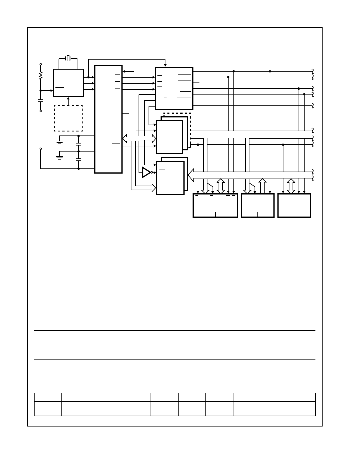
Functional Diagram
www.BDTIC.com/Intersil
80C86
RQ
TEST
INTR
NMI
/GT0, 1
HOLD
HLDA
EXECUTION UNIT
REGISTER FILE
DATA POINTER
AND
INDEX REGS
(8 WORDS)
16-BIT ALU
FLAGS
2
CLK RESET READY
BUS INTERFACE UNIT
SEGMENT REGISTERS
INSTRUCTION POINTER
BUS INTERFACE UNIT
CONTROL AND TIMING
MN/MX
RELOCATION
REGISTER FILE
AND
(5 WORDS)
6-BYTE
INSTRUCTION
QUEUE
2
3
3
GND
V
CC
4
16
3
4
LOCK
QS0, QS1
, S1, S0
S2
/S7
BHE
A19/S6
A16/S3
AD15-AD0
, RD, WR
INTA
DT/R, DEN, ALE, M/IO
BUS
INTERFACE
UNIT
EXECUTION
UNIT
MEMORY INTERFACE
B-BUS
ES
CS
SS
DS
IP
AH
BH
CH
DH
AL
BL
CL
DL
SP
BP
SI
DI
C-BUS
INSTRUCTION
STREAM BYTE
QUEUE
A-BUS
ARITHMETIC/
LOGIC UNIT
FLAGS
EXECUTION UNIT
CONTROL SYSTEM
142

80C86
www.BDTIC.com/Intersil
Pin Description
The following pin function descriptions are for 80C86 systems in either minimum or maximum mode. The “Local Bus” in these description is
the direct multiplexed bus interface connection to the 80C86 (without regard to additional bus buffers).
PIN
SYMBOL
AD15-AD0 2-16, 39 I/O ADDRESS DATA BUS: These lines constitute the time multiplexed memory/lO address (T1) and
NUMBER TYPE DESCRIPTION
data (T2, T3, TW, T4) bus. A0 is analogous to BHE
D0. It is LOW during Ti when a byte is to be transferred on the lower portion of the bus in memory
or I/O operations. Eight-bit oriented devices tied to the lower half would normally use A0 to condition chip select functions (See BHE
ance to the last valid logic level during interrupt acknowledge and local bus “hold acknowledge”
or “grant sequence”.
). These lines are active HIGH and are held at high imped-
for the lower byte of the data bus, pins D7-
A19/S6
A18/S5
A17/S4
A16/S3
/S7 34 O BUS HIGH ENABLE/STATUS: During T1 the bus high enable signal (BHE) should be used to
BHE
35-38 O ADDRESS/STA TUS: During T1, these are the four most significant address lines for memory op-
erations. During I/O operations these lines are LOW. During memory and I/O operations, status
information is available on these lines during T2, T3, TW, T4. S6 is always LOW. The status of
the interrupt enable FLAG bit (S5) is updated at the beginning of each clock cycle. S4 and S3
are encoded as shown.
This information indicates which segment register is presently being used for data accessing.
These lines are held at high impedance to the last valid logic level during local bus “hold ac-
knowledge” or “grant sequence”.
S4 S3 CHARACTERISTICS
0 0 Alternate Data
01Stack
1 0 Code or None
11Data
enable data onto the most significant half of the data bus, pins D15-D8. Eight bit oriented devices
tied to the upper half of the bus would normally use BHE
is LOW during T1 for read, write, and interrupt acknowledge cycles when a byte is to be transferred on the high portion of the bus. The S7 status information is available during T2, T3 and
T4. The signal is active LOW, and is held at high impedance to the last valid logic level during
interrupt acknowledge and local bus “hold acknowledge” or “grant sequence”, it is LOW during
T1 for the first interrupt acknowledge cycle.
BHE A0 CHARACTERISTICS
0 0 Whole Word
0 1 Upper Byte From/to Odd Address
1 0 Lower Byte From/to Even address
1 1 None
to condition chip select functions. BHE
RD
READY 22 I READY: is the acknowledgment from the addressed memory or I/O device that will complete the
32 O READ: Read strobe indicates that the processor is performing a memory or I/O read cycle, de-
pending on the state of the M/IO
the 80C86 local bus. RD
teed to remain HIGH in T2 until the 80C86 local bus has floated.
This line is held at a high impedance logic one state during “hold acknowledge” or “grand sequence”.
data transfer. The RDY signal from memory or I/O is synchronized by the 82C84A Clock Generator to form READY. This signal is active HIGH. The 80C86 READY input is not synchronized.
Correct operation is not guaranteed if the Setup and Hold Times are not met.
or S2 pin. This signal is used to read devices which reside on
is active LOW during T2, T3 and TW of any read cycle, and is guaran-
143

80C86
www.BDTIC.com/Intersil
Pin Description (Continued)
The following pin function descriptions are for 80C86 systems in either minimum or maximum mode. The “Local Bus” in these description is
the direct multiplexed bus interface connection to the 80C86 (without regard to additional bus buffers).
PIN
SYMBOL
INTR 18 I INTERRUPT REQUEST: is a level triggered input which is sampled during the last clock cycle
NUMBER TYPE DESCRIPTION
of each instruction to determine if the processor should enter into an interrupt acknowledge operation. A subroutine is vectored to via an interrupt vector lookup table located in system memory. It can be internally masked by software resetting the interrupt enable bit.
lNTR is internally synchronized. This signal is active HIGH.
TEST
NMI 17 I NON-MASKABLE INTERRUPT: is an edge triggered input which causes a type 2 interrupt. A
RESET 21 I RESET: causes the processor to immediately terminate it s present activity . The signal must tran-
CLK 19 I CLOCK: provide s the basic timing for the processor and bus controller. It is asymmetric with a
VCC 40 VCC: +5V power supply pin. A 0.1μF capacitor between pins 20 and 40 is recommended for de-
GND 1, 20 GND: Ground. Note: both must be connected. A 0.1μF capacitor between pins 1 and 20 is rec-
MN/MX
23 I TEST : input is examined by the “Wait” instruction. If the TEST input is LOW execution continues,
otherwise the processor waits in an “Idle” state. This input is synchronized internally during each
clock cycle on the leading edge of CLK.
subroutine is vectored to via an interrupt vector lookup table located in system memory. NMI is
not maskable internally by software. A transition from LOW to HIGH initiates the interrupt at the
end of the current instruction. This input is internally synchronized.
sition LOW to HIGH and remain active HIGH for at least four clock cycles. It restarts execution,
as described in the Instruction Set description, when RESET returns LOW. RESET is internally
synchronized.
33% duty cycle to provide optimized internal timing.
coupling.
ommended for decoupling.
33 I MINIMUM/MAXIMUM: Indicates what mode the processor is to operate in. The two modes are
discussed in the following sections.
Minimum Mode System
The following pin function descriptions are for the 80C86 in minimum mode (i.e., MN/MX = VCC). Only the pin functions which are unique to
minimum mode are described; all other pin functions are as described below.
SYMBOL
M/IO
WR
INTA
ALE 25 O ADDRESS LATCH ENABLE: is provided by the processor to latch the address into the
PIN
NUMBER TYPE DESCRIPTION
28 O STA TUS LINE: logically equivalent to S2 in the maximum mode. It is used to distinguish a mem-
29 O WRITE: indicates that the processor is performing a write memory or write I/O cycle, depending
24 O INTERRUPT ACKNOWLEDGE: is used as a read strobe for interrupt acknowledge cycles. It is
ory access from an I/O access. M/lO
valid until the final T4 of the cycle (M = HIGH, I/O = LOW). M/lO
one during local bus “hold acknowledge”.
on the state of the M/IO
LOW, and is held to high impedance logic one during local bus “hold acknowledge”.
active LOW during T2, T3 and TW of each interrupt acknowledge cycle. Note that INTA
floated.
82C82/82C83 address latch. It is a HIGH pulse active during clock LOW of T1 of any bus cycle.
Note that ALE is never floated.
signal. WR is active for T2, T3 and TW of any write cycle. It is active
becomes valid in the T4 preceding a bus cycle and remains
144
is held to a high impedance logic
is never

80C86
www.BDTIC.com/Intersil
Minimum Mode System (Continued)
The following pin function descriptions are for the 80C86 in minimum mode (i.e., MN/MX
minimum mode are described; all other pin functions are as described below.
= VCC). Only the pin functions which are unique to
SYMBOL
DT/R 27 O DATA TRANSMIT/RECEIVE: is needed in a minimum system that desires to use a data bus
DEN
HOLD
HLDA
PIN
NUMBER TYPE DESCRIPTION
transceiver. It is used to control the direction of data flow through the transceiver. Logically,
is equivalent to S1 in maximum mode, and its timing is the same as for M/IO (T = HIGH,
DT/R
R = LOW). DT/R
26 O DATA ENABLE: provided as an output enable for a bus transceiver in a minimum system which
uses the transceiver. DEN
cles. For a read or INTA
a write cycle it is active from the beginning of T2 until the middle of T4. DEN
impedance logic one during local bus “hold acknowledge”.
31, 30 I
O
HOLD: indicates that another master is requesting a local bus “hold”. To be an acknowledged,
HOLD must be active HIGH. The processor receiving the “hold” will issue a “hold acknowledge”
(HLDA) in the middle of a T4 or TI clock cycle. Simultaneously with the issuance of HLDA, the
processor will float the local bus and control lines. After HOLD is detected as being LOW, the
processor will lower HLDA, and when the processor needs to run another cycle, it will again drive
the local bus and control lines.
HOLD is not an asynchronous input. External synchronization should be provided if the system
cannot otherwise guarantee the setup time.
is held to a high impedance logic one during local bus “hold acknowledge”.
is active LOW during each memory and I/O access and for INTA cy-
cycle it is active from the middle of T2 u ntil the middle of T4, while for
is held to a high
Maximum Mode System
The following pin function descriptions are for the 80C86 system in maximum mode (i.e., MN/MX - GND). Only the pin functions which are
unique to maximum mode are described below.
SYMBOL
S0
S1
S2
PIN
NUMBER TYPE DESCRIPTION
26
27
28
O
O
O
STATUS: is active during T4, T1 and T2 and is returned to the passive state (1, 1, 1) during T3
or during TW when READY is HIGH. This status is used by the 82C88 Bus Controller to generate
all memory and I/O access control signals. Any change by S2
indicate the beginning of a bus cycle, and the return to the passive state in T3 or TW is used to
indicate the end of a bus cycle.
These signals are held at a high impedance logic one state during “grant sequence”.
S2 S1 S0 CHARACTERISTICS
0 0 0 Interrupt Acknowledge
0 0 1 Read I/O Port
0 1 0 Write I/O Port
011Halt
1 0 0 Code Access
1 0 1 Read Memory
1 1 0 Write Memory
111Passive
, S1 or S0 during T4 is used to
145

80C86
www.BDTIC.com/Intersil
Maximum Mode System (Continued)
The following pin function descriptions are for the 80C86 system in maximum mode (i.e., MN/MX
unique to maximum mode are described below.
- GND). Only the pin functions which are
SYMBOL
RQ/GT0
RQ/GT1
PIN
NUMBER TYPE DESCRIPTION
31, 30 I/O REQUEST/GRANT: pins are used by other local bus masters to force the processor to release
the local bus at the end of the processor’s current bus cycle. Each pin is bidirectional with
/GTO having higher priority than RQ/GT1. RQ/GT has an internal pull-up bus hold device so
RQ
it may be left unconnected. The request/grant sequence is as follows (see RQ
Timing)
1. A pulse of 1 CLK wide from another local bus master indicates a local bus request (“hold”)
to the 80C86 (pulse 1).
2. During a T4 or TI clock cycle, a pulse 1 CLK wide from the 80C86 to the requesting master
(pulse 2) indicates that the 80C86 has allowed the local bus to float and that it will enter the
“grant sequence” state at the next CLK. The CPU’s bus interface unit is disconnected logically from the local bus during “grant sequence”.
3. A pulse 1 CLK wide from the requesting master indicates to the 80C86 (pulse 3) that the
“hold” request is about to end and that the 80C86 can reclaim the local bus at the next CLK.
The CPU then enters T4 (or TI if no bus cycles pending).
Each Master-Master exchange of the local bus is a sequence of 3 pulses. There must be one
idle CLK cycle after each bus exchange. Pulses are active low.
If the request is made while the CPU is performing a memory cycle, it will release the local
bus during T4 of the cycle when all the following conditions are met:
1. Request occurs on or before T2.
2. Current cycle is not the low byte of a word (on an odd address).
3. Current cycle is not the first acknowledge of an interrupt acknowledge sequence.
4. A locked instruction is not currently executing.
If the local bus is idle when the request is made the two possible events will follow:
1. Local bus will be released during the next cycle.
2. A memory cycle will st art within three clocks. Now the four rules for a currently active memory
cycle apply with condition number 1 already satisfied.
/GT Sequence
LOCK
QS1, QSO 24, 25 O QUEUE STATUS: The queue status is valid during the CLK cycle after which the queue opera-
29 O LOCK: output indicates that other system bus masters are not to gain control of the system bus
while LOCK
remains active until the completion of the next instruction. This signal is active LOW, and is held
at a high impedance logic one state during “grant sequence”. In MAX mode, LOCK
ically generated during T2 of the first INTA
cycle.
tion is performed.
QS1 and QS0 provide status to allow external tracking of the internal 80C86 instruction queue.
Note that QS1, QS0 never become high impedance.
is active LOW. The LOCK signal is activated by the “LOCK” prefix instruction and
is automat-
cycle and removed during T2 of the second INTA
QSI QSO
0 0 No Operation
0 1 First byte of op code from queue
1 0 Empty the queue
1 1 Subsequent byte from queue
146

80C86
www.BDTIC.com/Intersil
Functional Description
Static Operation
All 80C86 circuitry is of static design. Internal registers,
counters and latches are static and require no refresh as
with dynamic circuit design. This eliminates the minimum
operating frequency restriction placed on other microprocessors. The CMOS 80C86 can operate from DC to the specified upper frequency limit. The processor clock may be
stopped in either state (HIGH/LOW) and held there indefinitely. This type of operation is especially useful for system
debug or power critical applications.
The 80C86 can be single stepped using only the CPU clock.
This state can be maintained as long as is necessary. Single
step clock operation allows simple interface circuitry to provide critical information for bringing up your system.
Static design also allows very low frequency operation (down
to DC). In a power critical situation, this can provide
extremely low power operation since 80C86 power dissipation is directly related to operating frequency. As the system
frequency is reduced, so is the operating power until, ultimately, at a DC input frequency, the 80C86 power requirement is the standby current, (500μA maximum).
Internal Architecture
The internal functions of the 80C86 processor are partitioned
logically into two processing units. The first is the Bus Interface Unit (BlU) and the second is the Execution Unit (EU) as
shown in the CPU functional diagram.
These units can interact directly, but for the most part perform
as separate asynchronous operational processors. The bus
interface unit provides the functions related to instruction
fetching and queuing, operand fetch and store, and address
relocation. This unit also provides the basic bus control. The
overlap of instruction pre-fetching provided by this unit serves
to increase processor performance through improved bus
bandwidth utilization. Up to 6 bytes of the instruction stream
can be queued while waiting for decoding and execution.
The instruction stream queuing mechanism allows the BIU to
keep the memory utilized very efficiently. Whenever there is
space for at least 2 bytes in the queue, the BlU will attempt a
word fetch memory cycle. This greatly reduces “dead-time”
on the memory bus. The queue acts as a First-In-First-Out
(FIFO) buffer, from which the EU extracts instruction bytes
as required. If the queue is empty (following a branch
instruction, for example), the first byte into the queue immediately becomes available to the EU.
The execution unit receives pre-fetched instructions from the
BlU queue and provides un-relocated operand addresses to
the BlU. Memory operands are passed through the BIU for processing by the EU, which passes results to the BIU for storage.
Memory Organization
The processor provides a 20-bit address to memory, which
locates the byte being referenced. The memory is organized
as a linear array of up to 1 million bytes, addressed as
00000(H) to FFFFF(H). The memory is logically divided i nto
code, data, extra and stack segments of up to 64K bytes
each, with each segment falling on 16-byte boundaries. (See
Figure 1).
FFFFFH
64K-BIT
+ OFFSET
SEGMENT
REGISTER FILE
CS
SS
DS
ES
FIGURE 1. 80C86 MEMORY ORGANIZATION
TABLE 1.
TYPE OF
MEMORY
REFERENCE
Instruction Fetch CS None IP
Stack Operation SS None SP
Variable (except
following)
String Source DS CS, ES, SS SI
String Destination ES None DI
BP Used As Base
Register
DEFAULT
SEGMENT
BASE
DS CS, ES, SS Effective
SS CS, DS, ES Effective
ALTERNATE
SEGMENT
CODE SEGMENT
XXXXOH
STACK SEGMENT
DATA SEGMENT
EXTRA SEGMENT
00000H
BASE OFFSET
Address
Address
All memory references are made relative to base addresses
contained in high speed segment registers. The segment
types were chosen based on the addressing needs of programs. The segment register to be selected is automatica lly
chosen according to the specific rules of Table 1. All information in one segment type share the same logical attributes
(e.g. code or data). By structuring memory into re-locatable
areas of similar characteristics and by automatically selecting segment registers, programs are shorter, faster and
more structured. (See Table 1).
Word (16-bit) operands can be located on even or odd
address boundaries and are thus, not constrained to even
boundaries as is the case in many 16-bit computers. For
address and data operands, the least significant byte of the
word is stored in the lower valued address location and the
most significant byte in the next higher address location. The
BIU automatically performs the
proper number of memory
147

80C86
www.BDTIC.com/Intersil
accesses; one, if the word operand is on an even byte
boundary and two, if it is on an odd byte boundary. Except
for the performance penalty, this double access is transparent to the software. The performance penalty does not occur
for instruction fetches; only word operands.
Physically, the memory is organized as a high bank (D15D8) and a low bank (D7-D0) of 512K bytes addressed in parallel by the processor’s address lines.
Byte data with even addresses is transferred on the D7-D0
bus lines, while odd addressed byte data (A0 HIGH) is transferred on the D15-D8 bus lines. The processor provides two
enable signals, BHE and A
from or writing into either an odd byte location, even byte
location, or both. The instruction stream is fetched from
memory as words and is addressed internally by the processor at the byte level as necessary.
In referencing word data, the BlU requires o ne or two memory
cycles depending on whether the starting byte of the word is
on an even or odd address, respectively. Consequently, in re ferencing word operands performance can be optimized by
locating data on even address boundaries. This is an especially useful technique for using the stack, since odd address
references to the stack may adversely affect the context
switching time for interrupt processing or task multiplexing.
Certain locations in memory are reserved for specific CPU
operations (See Figure 2). Locations from address FFFF0H
through FFFFFH are reserved for operations including a jump
to the initial program loading routine. Following RESET, the
CPU will always begin execution at location FFFF0H where
the jump must be located. Locations 00000H through 003FFH
are reserved for interrupt operations. Each of the 256 possible
interrupt service routines is accessed thru its own pair of 16bit pointers (segment address pointer and offset address
pointer). The first pointer, used as the offset address, is
loaded into the lP and the second pointer, which designates
the base address is loaded into the CS. At this point program
control is transferred to the interrupt routine. The pointer elements are assumed to have been stored at the respective
places in reserved memory prior to occurrence of interrupts.
Minimum and Maximum Operation Modes
The requirements for supporting minimum and maximum
80C86 systems are sufficiently different that they cannot be
met efficiently using 40 uniquely defined pins. Consequently,
the 80C86 is equipped with a strap pin (MN/MX
defines the system configuration. The definition of a certain
subset of the pins changes, dependent on the condition of the
strap pin. When the MN/MX
80C86 defines pins 24 through 31 and 34 in maximum mode.
When the MN/MX
ates bus control signals itself on pins 24 through 31 and 34.
The minimum mode 80C86 can be used with either a multiplexed or demultiplexed bus. This architecture provides the
80C86 processing power in a highly integrated form.
The demultiplexed mode requires two 82C82 latches (for 64K
addressability) or three 82C82 latches (for a full megabyte of
addressing). An 82C86 or 82C87 transceiver can also be
used if data bus buffering is required. (See Figure 6A.) The
pin is strapped to VCC, the 80C86 gener-
, to selectively allow reading
0
) which
pin is strapped to GND, the
80C86 provides DEN
ALE to latch the addresses. This configuration of the minimum
mode provides the standard demultiplexed bus structure with
heavy bus buffering and relaxed bus timing requirement s.
The maximum mode employs the 82C88 bus controller (See
Figure 6B). The 82C88 decodes status lines S0
and provides the system with all bus control signals.
Moving the bus control to the 82C88 provides better source
and sink current capability to the control lines, and frees the
80C86 pins for extended large system features. Hardware
lock, queue status, and two request/grant interfaces are provided by the 80C86 in maximum mode. Thes e feat ures al low
coprocessors in local bus and remote bus configurations.
Bus Operation
The 80C86 has a combined address and data bus commonly referred to as a time multiplexed bus. This technique
provides the most efficient use of pins on the processor
while permitting the use of a standard 40 lead package. This
“local bus” can be buffered directly and used throughout the
system with address latching provided on memory and I/O
modules. In addition, the bus can also be demultiplexed at
the processor with a single set of 82C82 address latches if a
standard non-multiplexed bus is desired for the system.
Each processor bus cycle consists of at least four CLK
cycles. These are referred to as T1, T2, T3 and T4 (see Figure 3). The address is emitted from the proce ssor during T1
and data transfer occurs on the bus during T3 and T4. T2 is
used primarily for changing the direction of the bus during
read operations. In the event that a “NOT READY” indication
is given by the addressed device, “Wait” states (TW) are
inserted between T3 and T4 . Each inserted wait state is the
same duration as a CLK cycle. Periods can occur between
80C86 driven bus cycles. These are referred to as idle”
states (T
cycles for internal housekeeping and processing.
During T1 of any bus cycle, the ALE (Address Latch Enable)
signal is emitted (by either the processor or the 82C88 bus
controller, depending on the MN/MX
edge of this pulse, a valid address and certain status information for the cycle may be latched.
Status bits S0
maximum mode, to identify the type of bus transaction
according to Table 2.
) or inactive CLK cycles. The processor uses these
I
S2
0 0 0 Interrupt
0 0 1 Read I/O
010Write I/O
011Halt
1 0 0 Instruction Fetch
1 0 1 Read Data from Memory
1 1 0 Write Data to Memory
1 1 1 Passive (No Bus Cycle)
S1 S0 CHARACTERISTICS
and DT/R to control the transceiver, and
, S1 and S2,
strap). At the trailing
, S1 and S2 are used by the bus controller, in
TABLE 2.
148

80C86
www.BDTIC.com/Intersil
Status bits S3 through S7 are time multiplexed with high
order address bits and the BHE signal, and are therefore
valid during T2 through T4. S3 and S4 indicate which segment register (see Instruction Set Description) was used for
this bus cycle in forming the address, according to Table 3.
S5 is a reflection of the PSW interrupt enable bit. S3 is
always zero and S7 is a spare status bit.
TABLE 3.
S4 S3 CHARACTERISTICS
0 0 Alternate Data (Extra Segment)
01Stack
1 0 Code or None
11Data
FFFFFH
FFFF0H
3FFH
3FCH
RESET BOOTSTRAP
PROGRAM JUMP
TYPE 225 POINTER
(AVAILABLE)
I/O Addressing
In the 80C86, I/O operations can address up to a maximum
of 64K I/O byte registers or 32K I/O word registers. The I/O
address appears in the same format as the memory address
on bus lines A15-A0. The address lines A19-A16 are zero in
I/O operations. The variable I/O instructions which use register DX as a pointer have full address capability while the
direct I/O instructions directly address one or two of the 256
I/O byte locations in page 0 of the I/O address space.
I/O ports are addressed in the same manner as memory locations. Even addressed bytes are transferred on the D7-D0 bus
lines and odd addressed bytes on D15-D8. Care must be taken
to ensure that each register within an 8-bit peripheral located on
the lower portion of the bus be addressed as even.
AVAILABLE
INTERRUPT
POINTERS
(224)
RESERVED
INTERRUPT
POINTERS
(27)
DEDICATED
INTERRUPT
POINTERS
(5)
TYPE 33 POINTER
084H
080H
07FH
014H
010H
00CH
008H
004H
000H
(AVAILABLE)
TYPE 32 POINTER
(AVAILABLE)
TYPE 31 POINTER
(AVAILABLE)
TYPE 5 POINTER
(RESERVED)
TYPE 4 POINTER
OVERFLOW
TYPE 3 POINTER
1 BYTE INT INSTRUCTION
TYPE 2 POINTER
NON MASKABLE
TYPE 1 POINTER
SINGLE STEP
TYPE 0 POINTER
DIVIDE ERROR
CS BASE ADDRESS
IP OFFSET
16 BITS
FIGURE 2. RESERVED MEMORY LOCATIONS
149

80C86
www.BDTIC.com/Intersil
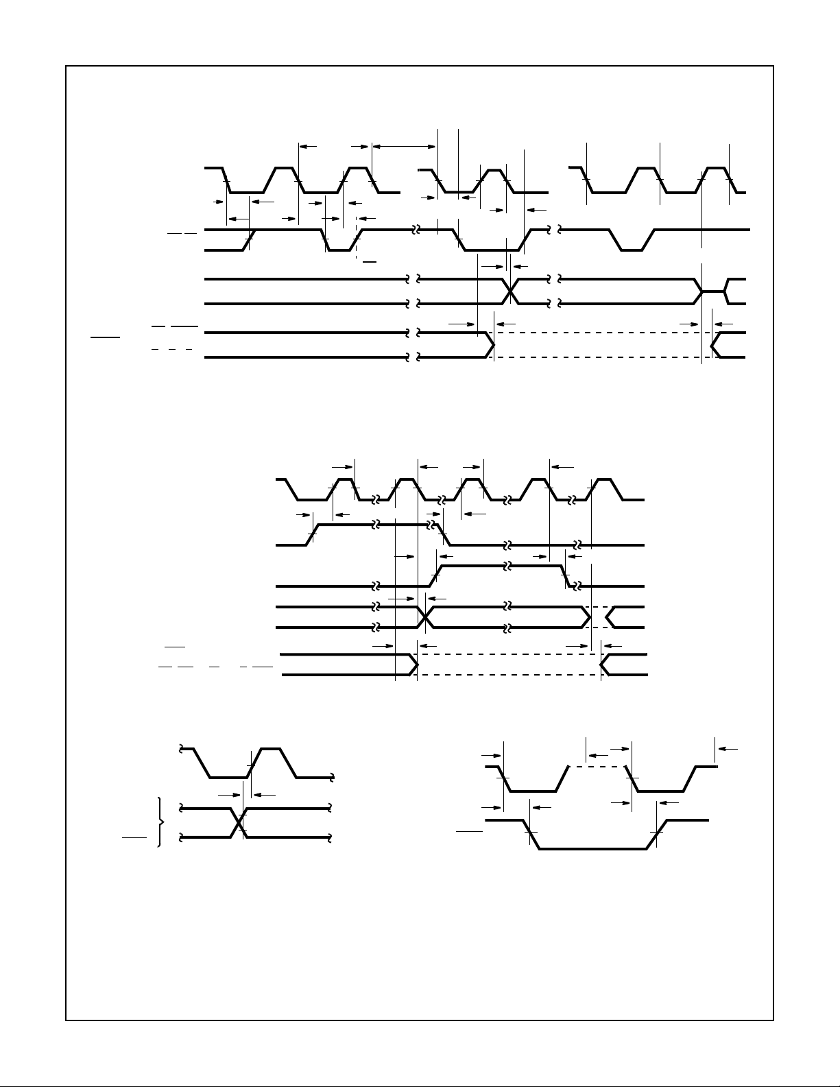
CLK
ALE
S
2-S0
ADDR/
STATUS
ADDR/DATA
(4 + NWAIT) = TCY
T1 T2 T3 T4TWAIT T1 T2 T3 T4TWAIT
BHE,
A19-A16
A15-A0
BUS RESERVED
FOR DATA IN
S7-S3
D15-D0
VALID
A19-A16
A15-A0 DATA OUT (D15-D0)
(4 + NWAIT) = TCY
GOES INACTIVE IN THE STATE
JUST PRIOR TO T
BHE
S7-S3
4
RD
, INTA
READY
READYREADY
WAIT WAIT
DT/R
DEN
MEMORY ACCESS TIME
WR
FIGURE 3. BASIC SYSTEM TIMING
150

80C86
www.BDTIC.com/Intersil
External Interface
Processor RESET and Initialization
Processor initialization or start up is accomplished with activation (HIGH) of the RESET pin. The 80 C86 RESET is require d to
be HIGH for greater than 4 CLK cycles. The 80C86 will terminate operations on the high-going edge of RESET and will
remain dormant as long as RESET is HIGH. The low-going
transition of RESET triggers an internal reset sequence for
approximately 7 clock cycles. After this interval, the 80C86
operates normally beginning with the instruction in absolute
location FFFF0H. (See Figure 2). The RESET input is internally
synchronized to the processor clock. At initialization, the HIGHto-LOW transition of RESET must occur no sooner than 50 μs
(or 4 CLK cycles, whichever is greater) after power-up, to allow
complete initialization of the 80C86.
NMl will not be recognized prior to the second CLK cycle following the end of RESET. If NMl is asserted sooner than nine clock
cycles after the end of RESET, the processor may execute one
instruction before responding to the interrupt.
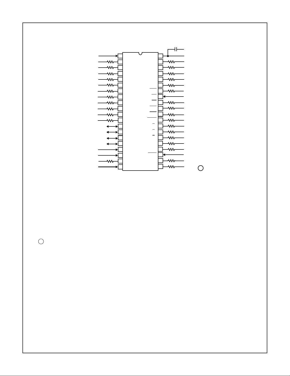
Bus Hold Circuitry
To avoid high current conditions caused by floating inputs to
CMOS devices and to eliminate need for pull-up/down resistors,
“bus-hold” circuitry has been used on the 80C86 pins 2-16, 2632 and 34-39. (See Figure 4A and Figure 4B). These circuits
will maintain the last valid logic state if no driving source is
present (i.e., an unconnected pin or a driving sourc e which goes
to a high impedance state). To overdrive the “bus hold” circuits,
an external driver must be capable of supplying approximately
400μA minimum sink or source current at valid input voltage
levels. Since this “bus hold” circuitry is active and not a “res istive” type element, the associated power supply current is negligible and power dissipation is significantly reduced when
compared to the use of passive pu ll-up res isto rs.
BOND
PAD
EXTERNAL
OUTPUT
DRIVER
PIN
Interrupt Operations
Interrupt operations fall into two classes: software or hard-
ware initiated. The software initiated interrupts and software
aspects of hardware interrupts are specified in the Instruction Set Description. Hardware interrupts can be classified
as non-maskable or maskable.
Interrupts result in a transfer of control to a new program location. A 256-element table containing address pointers to the
interrupt service program locations resides in absolute locations 0 through 3FFH, which are reserved for this purpose.
Each element in the table is 4 bytes in size and corresponds
to an interrupt “type”. An interrupting device supplies an 8-bit
type number during the interrupt acknowledge sequence,
which is used to “vector” through the appropriate element to
the new interrupt service program location. All flags and both
the Code Segment and Instruction Pointer register are saved
as part of the lNTA
sequence. These are restored upon exe-
cution of an Interrupt Return (IRET) instruction.
Non-Maskable Interrupt (NMI)
The processor provides a single non-maskable interrupt pin
(NMI) which has higher priority than the maskable interrupt
request pin (INTR). A typical use would be to activate a
power failure routine. The NMI is edge-triggered on a LOWto-HIGH transition. The activation of this pin causes a type 2
interrupt.
NMl is required to have a duration in the HIGH state of
greater than two CLK cycles, but is not required to be synchronized to the clock. Any positive transition of NMI is
latched on-chip and will be serviced at the end of the current
instruction or between whole moves of a block-type instruction. Worst case response to NMI would be for multiply,
divide, and variable shift instructions. There is no specification on the occurrence of the low-going edge; it may occur
before, during or after the servicing of NMI. Another positive
edge triggers another response if it occurs after the start of
the NMI procedure. The signal must be free of logical spikes
in general and be free of bounces on the low-goin g edge to
avoid triggering extraneous responses.
INPUT
BUFFER
INPUT
PROTECTION
CIRCUITRY
Maskable Interrupt (INTR)
The 80C86 provides a single interrupt request input (lNTR)
which can be masked internally by software with the rese tting of the interrupt enable flag (IF) status bit. The interrupt
FIGURE 4A. BUS HOLD CIRCUITRY PIN 2-16, 34-39
request signal is level triggered. It is internally syn chronized
during each clock cycle on the high-going edge of CLK. To
be responded to, lNTR must be present (HIGH) during the
clock period preceding the end of the current instruction or
the end of a whole move for a block type instruction. lNTR
may be removed anytime after the falling edge of the first
signal. During the interrupt response sequence further
INTA
interrupts are disabled. The enable bit is reset as part of the
response to any interrupt (lNTR, NMI, software interrupt or
single-step), although the FLAGS register which is automatically pushed onto the stack reflects the state of the processor prior to the interrupt. Until the old FLAGS register is
restored, the enable bit will be zero unless specifically set by
PV
OUTPUT
DRIVER
BUFFER
CC
INPUT
INPUT
PROTECTION
CIRCUITRY
FIGURE 4B. BUS HOLD CIRCUITRY PIN 26-32
BOND
PAD
EXTERNAL
PIN
an instruction.
151

80C86
www.BDTIC.com/Intersil
During the response sequence (Figure 5) the processor executes two successive (back-to-back) interrupt acknowledge
cycles. The 80C86 emits the LOCK
signal (Max mode only)
from T2 of the first bus cycle until T2 of the second. A local
bus “hold” request will not be honored until the end of the
second bus cycle. In the second bus cycle, a byte is supplied
to the 80C86 by the 82C59A Interrupt Controller, which identifies the source (type) of the interrupt. This byte is multiplied
by four and used as a pointer into the interrupt vector lookup
table. An INTR signal left HIGH will be continually responded
to within the limitations of the enable bit and sample period.
The INTERRUPT RETURN instruction includes a FLAGS
pop which returns the status of the original interrupt enabl e
bit when it restores the FLAGS.
T1 T2 T3 T4 TI
ALE
LOCK
INTA
AD0-
AD15
FLOAT
FIGURE 5. INTERRUPT ACKNOWLEDGE SEQUENCE
T1
T2
T3
TYPE
VECTOR
T4
Halt
When a software “HALT” instruction is executed the processor indicates that it is entering the “HALT” state in one of two
ways depending upon which mode is strapped. In minimum
mode, the processor issues one ALE with no qualifying bus
control signals. In maximum mode the processor issues
appropriate HALT status on S2
, S1, S0 and the 82C88 bus
controller issues one ALE. The 80C86 will not leave the
“HALT” state when a local bus “hold” is entered while in
“HALT”. In this case, the processor reissues the HALT indicator at the end of the local bus hold. An NMI or interrupt
request (when interrupts enabled) or RESET will force the
80C86 out of the “HALT” state.
Read/Modify/Write (Semaphore)
Operations Via Lock
The LOCK status information is provided by the processor
when consecutive bus cycles are required during the execution
of an instruction. This gives the processor the capability of performing read/modify/write operations on memory (via the
Exchange Register With Memory instruction, for example) without another system bus master receiving intervening memory
cycles. This is useful in multiprocessor system configurations to
accomplish “test and set lock” operations. The LOCK signal is
activated (forced LOW) in the clock cycle following decoding of
the software “LOCK” prefix instruction. It is deactivated at the
end of the last bus cycle of the instruction following the “LOCK”
prefix instruction. While LOCK is active a request on a RQ/GT
pin will be recorded and then honored at the end of the LOCK.
External Synchronization Via TEST
As an alternative to interrupts, the 80C86 provides a single
software-testable input pin (TEST
). This input is utilized by
executing a WAIT instruction. The single WAIT instruction is
repeatedly executed until the TEST
input goes active (LOW).
The execution of WAIT does not consume bus cycles once
the queue is full.
If a local bus request occurs during WAIT execution, the
80C86 three-states all output drivers while inputs and I/O
pins are held at valid logic levels by internal bus-hold circuits. If interrupts are enabled, the 80C86 will recognize
interrupts and process them when it regains control of the
bus. The WAIT instruction is then refetched, and re-executed.
TABLE 4. 80C86 REGISTER
AH AL
AX
BX
BH
CH
CX
DX
DH
FLAGSHFLAGS
SP
BP
SI
DI
IP
CS
DS
SS
ES
ACCUMULATOR
BASE
BL
CL
COUNT
DATA
DL
STACK POINTER
BASE POINTER
SOURCE INDEX
DESTINATION INDEX
INSTRUCTION POINTER
L
STATUS FLAG
CODE SEGMENT
DATA SEGMENT
STACK SEGMENT
EXTRA SEGMENT
Basic System Timing
Typical system configurations for the processor operating in
minimum mode and in maximum mode are shown in Figures
6A and 6B, respectively. In minimum mode, the MN/MX
pin
is strapped to VCC and the processor emits bus control signals (e.g. RD
MN/MX
, WR, etc.) directly. In maximum mode, the
pin is strapped to GND and the processor emits
coded status information which the 82C88 bus controller
uses to generate MULTIBUS compatible bus control signals.
Figure 3 shows the signal timing relationships.
System Timing - Minimum System
The read cycle begins in T1 with the assertion of the
Address Latch Enable (ALE) signal. The trailing (low-going)
edge of this signal is used to latch the address information,
which is valid on the address/data bus (AD0-AD15) at this
time, into the 82C82/82C83 latch. The BHE
and A0 signals
address the low, high or both bytes. From T1 to T4 the M/lO
signal indicates a memory or I/O operation. At T2, the
address is removed from the address/data bus and the bus
152

80C86
www.BDTIC.com/Intersil
is held at the last valid logic state by internal bus hold
devices. The read control signal is also asserted at T2. The
read (RD) signal causes the addressed device to enable its
data bus drivers to the local bus. Some time later, valid data
will be available on the bus and the addressed device will
drive the READY line HIGH. When the processor returns the
read signal to a HIGH level, the addressed device will again
three-state its bus drivers. If a transceiver (82C86/82C87) is
required to buffer the 80C86 local bus, signals DT/R and
are provided by the 80C86.
DEN
A write cycle also begins with the assertion of ALE and the
emission of the address. The M/IO
to indicate a memory or I/O write operation. In T2, immediately following the address emission, the processor emits
the data to be written into the addressed location. This data
remains valid until at least the middle of T4. During T2, T3
and TW, the processor asserts the write control signal. The
write (WR
opposed to the read which is delayed somewhat into T2 to
provide time for output drivers to become inactive.
) signal becomes active at the beginning of T2 as
signal is again asserted
The BHE
byte(s) of the memory/lO word to be read or written according to Table 5.
I/O ports are addressed in the same manner as memory
location. Even addressed bytes are transferred on the D7D0 bus lines and odd address bytes on D15-D8.
The basic difference between the interrupt acknowledge
cycle and a read cycle is that the interrupt acknowledge signal (INTA
the address bus is held at the last valid logic state by internal
bus hold devices. (See Figure 4). In the second of two successive INTA
data bus (D7-D0) as supplied by the interrupt system logic
(i.e., 82C59A Priority Interrupt Controller). This byte identifies the source (type) of the interrupt. It is multiplied by four
and used as a pointer into an interrupt vector lookup table,
as described earlier.
and A0 signals are used to select the proper
TABLE 5.
BHE
00Whole word
0 1 Upper Byte From/To Odd Address
1 0 Lower Byte From/To Even Address
1 1 None
A0 CHARACTERISTICS
) is asserted in place of the read (RD) signal and
cycles a byte of information is read from the
153

80C86
www.BDTIC.com/Intersil
Bus Timing - Medium Size Systems
For medium complexity systems the MN/MX
pin is connected to GND and the 82C88 Bus Controller is added to the
system as well as an 82C82/82C83 latch for latching the
system address, and an 82C86/82C87 transceiver to allow
for bus loading greater than the 80C86 is capable of handling. Signals ALE, DEN
, and DT/R are generated by the
82C88 instead of the processor in this configuration,
although their timing remains relatively the same. The
80C86 status outputs (S2
, S1 and S0) provide type-of-cycle
information and become 82C88 inputs. This bus cycle information specifies read (code, data or I/O), write (data or I/O),
interrupt acknowledge, or software halt. The 82C88 issues
control signals specifying memory read or write, I/O read or
write, or interrupt acknowledge. The 82C88 provides two
V
CC
GND
V
CC
82C8A/85
CLOCK
GENERATOR
RES
RDY
WAIT
STATE
GENERATOR
C1
C2
C1 = C2 = 0.1μF
GND
1
20
40
CLK
READY
RESET
80C86
CPU
AD0-AD15
GND
V
CC
MN/MX
M/IO
INTA
RD
WR
DT/R
DEN
ALE
A16-A19
BHE
V
CC
GND
ADDR/DATA
STB
OE
82C82
LATCH
2 OR 3
T
OE
82C86
TRANSCEIVER
types of write strobes, normal and advanced, to be applied
as required. The normal write strobes have data valid at the
leading edge of write. The advanced write strobes have the
same timing as read strobes, and hence, data is not valid at
the leading edge of write. The 82C86/82C87 transceiver
receives the usual T and OE
inputs from the 82C88 DT/R
and DEN signals.
The pointer into the interrupt vector table, which is passed
during the second INTA
cycle, can be derived from an
82C59A located on either the local bus or the system bus. If
the master 82C59A Priority Interrupt Controller is positioned
on the local bus, the 82C86/82C87 transceiver must be disabled when reading from the master 82C59A during the
interrupt acknowledge sequence and software “poll”.
ADDR
DATA
(2)
BHE
A0
E
E
H
OPTIONAL
FOR INCREASED
DATA BUS DRIVE
HM-6516
CMOS RAM
2K x 8
L
FIGURE 6A. MINIMUM MODE 80C86 TYPICAL CONFIGURATION
154
W
2K x 8
G
CMOS PROM (2)
2K x 8 2K x 8
E G
HM-6616
RDWR
CS
CMOS
82CXX
PERIPHERALS
80C86
www.BDTIC.com/Intersil
V
CC
CLK
S0
S1
S2
DEN
DT/R
ALE
STB
OE
(2 OR 3)
T
OE
TRANSCEIVER
82C88
BUS
CTRLR
82C82
82C86
(2)
MRDC
MWTC
AMWC
AIOWC
IORC
IOWC
INTA
BHE
E
H
2K x 8
NC
NC
ADDR
DATA
A0
E
L
HM-65162
CMOS RAM
2K x 8
W G
E G
HM-6616
CMOS PROM (2)
2K x 8 2K x 8
RDWR
CS
CMOS
82CXX
PERIPHERALS
GND
V
CC
82C84A/85
CLOCK
GENERATOR/
RES
RDY
WAIT
STATE
GENERATOR
C1
C2
C1 = C2 = 0.1μF
GND
1
20
40
MN/MX
CLK
READY
RESET
80C86
CPU
AD0-AD15
A16-A19
GND
V
CC
S0
S1
S2
LOCK
BHE
GND
NC
GND
ADDR/DATA
FIGURE 6B. MAXIMUM MODE 80C86 TYPICAL CONFIGURATION
Absolute Maximum Ratings Thermal Information
Supply Voltage . . . . . . . . . . . . . . . . . . . . . . . . . . . . . . . . . . . . .+8.0V
Input, Output or I/O Voltage . . . . . . . . . . . .GND -0.5V to V
Storage Temperature Range . . . . . . . . . . . . . . . . . -65
Junction Temperature
Ceramic Packages . . . . . . . . . . . . . . . . . . . . . . . . . . . . . . +175
Plastic Packages. . . . . . . . . . . . . . . . . . . . . . . . . . . . . . . . +150
Lead Temperature (Soldering 10s). . . . . . . . . . . . . . . . . . . . +300
+0.5V
CC
o
C to +150oC
o
o
o
Thermal Resistance (Typical, Note 1) θ
PDIP Package. . . . . . . . . . . . . . . . . . . 50 N/A
PLCC Package . . . . . . . . . . . . . . . . . . 46 N/A
SBDIP Package. . . . . . . . . . . . . . . . . . 30 6
C
CLCC Package . . . . . . . . . . . . . . . . . . 40 6
C
Gate Count . . . . . . . . . . . . . . . . . . . . . . . . . . . . . . . . . . .9750 Gates
C
(oC/W) θJC (oC/W)
JA
(Lead tips only for surface mount packages)
ESD Classification . . . . . . . . . . . . . . . . . . . . . . . . . . . . . . . . Class 1
CAUTION: Stresses above those listed in “Absolute Maximum Ratings” may cause permanent damage to the device. This is a stress only rating and operation
of the device at these or any other conditions above those indicated in the operational sections of this specification is not implied.
NOTE:
is measured with the component mounted on an evaluation PC board in free air.
1. θ
JA
Operating Conditions
Operating Supply Voltage. . . . . . . . . . . . . . . . . . . . . +4.5V to +5.5V
M80C86-2 ONLY. . . . . . . . . . . . . . . . . . . . . . . . +4.75V to +5.25V
Operating Temperature Range: C80C86/-2 . . . . . . . . 0oC to +70oC
I80C86/-2. . . . . . . . . . . . . . . . . . . . . . . . . . . . . . . .-40
M80C86/-2. . . . . . . . . . . . . . . . . . . . . . . . . . . . . .-55
o
C to +85oC
o
C to +125oC
DC Electrical Specifications V
= 5.0V, ±10%; TA = 0oC to +70oC (C80C86, C80C86-2)
CC
= 5.0V, ±10%; TA = -40oC to +85oC (l80C86, I80C86-2)
V
CC
= 5.0V, ±10%; TA = -55oC to +125oC (M80C86)
V
CC
= 5.0V, ±5%; TA = -55oC to +125oC (M80C86-2)
V
CC
SYMBOL PARAMETER MIN MAX UNITS TEST CONDITION
V
lH
Logical One
Input Voltage
2.0
2.2
155
V
V
C80C86, I80C86 (Note 5)
M80C86 (Note 5)

80C86
www.BDTIC.com/Intersil
DC Electrical Specifications V
= 5.0V, ±10%; TA = 0oC to +70oC (C80C86, C80C86-2)
CC
= 5.0V, ±10%; TA = -40oC to +85oC (l80C86, I80C86-2)
V
CC
= 5.0V, ±10%; TA = -55oC to +125oC (M80C86)
V
CC
= 5.0V, ±5%; TA = -55oC to +125oC (M80C86-2)
V
CC
SYMBOL PARAMETER MIN MAX UNITS TEST CONDITION
V
V
IHC
V
ILC
V
OH
V
l
BHH
l
BHL
I
I
CCSB
I
CCOP
Capacitance T
Logical Zero Input Voltage 0.8 V
IL
CLK Logical One Input Voltage VCC -0.8 V
CLK Logical Zero Input Voltage 0.8 V
Output High Voltage 3.0
-0.4
V
CC
Output Low Voltage 0.4 V lOL = +2.5mA
OL
Input Leakage Current -1.0 1.0 μAVIN = GND or VCC DIP
I
I
V
V
l
= -2.5mA
OH
= -100μA
l
OH
Pins 17-19, 21-23, 33
Input Current-Bus Hold High -40 -400 μAVIN = - 3.0V (Note 1)
Input Current-Bus Hold Low 40 400 μAVIN = - 0.8V (Note 2)
Output Leakage Current - -10.0 μAV
O
= GND (Note 4)
OUT
Standby Power Supply Current - 500 μAVCC = - 5.5V (Note 3)
Operating Power Supply Current - 10 mA/MHz FREQ = Max, VIN = VCC or GND,
Outputs Open
= 25oC
A
SYMBOL PARAMETER TYPICAL UNITS TEST CONDITIONS
C
C
OUT
C
Input Capacitance 25 pF FREQ = 1MHz. All measurements are referenced to device GND
IN
Output Capacitance 25 pF FREQ = 1MHz. All measurements are referenced to device GND
I/O Capacitance 25 pF FREQ = 1MHz. All measurements are referenced to device GND
I/O
NOTES:
2. lBHH should be measured after raising V
3. IBHL should be measured after lowering V
4. lCCSB tested during clock high time after halt instruction executed. V
5. IO should be measured by putting the pin in a high impedance state and then driving V
6. MN/MX
is a strap option and should be held to VCC or GND.
to VCC and then lowering to 3.0V on the following pins 2-16, 26-32, 34-39.
IN
to GND and then raising to 0.8V on the following pins: 2-16, 34-39.
IN
= VCC or GND, VCC = 5.5V, Outputs unloaded.
IN
to GND on the following pins: 26-29 and 32.
OUT
AC Electrical Specifications V
= 5.0V ±10%; TA = 0oC to +70oC (C80C86, C80C86-2)
CC
5.0V ±100%; TA = -40oC to +85oC (I80C86, I80C86-2)
V
CC =
= 5.0V ±100%; TA = -55oC to +125oC (M80C86)
V
CC
= 5.0V ±5%; TA = -55oC to +125oC (M80C86-2)
V
CC
MINIMUM COMPLEXITY SYSTEM
80C86 80C86-2
SYMBOL PARAMETER
TIMING REQUIREMENTS
(1) TCLCL Cycle Period 200 125 ns
(2) TCLCH CLK Low Time 118 68 ns
(3) TCHCL CLK High Time 69 44 ns
(4) TCH1CH2 CLK Rise Time 10 10 ns From 1.0V to 3.5V
(5) TCL2C1 CLK FaIl Time 10 10 ns From 3.5V to 1.0V
156
UNITS
TEST
CONDITIONSMIN MAX MIN MAX

80C86
www.BDTIC.com/Intersil
AC Electrical Specifications V
MINIMUM COMPLEXITY SYSTEM
SYMBOL PARAMETER
(6) TDVCL Data In Setup Time 30 20 ns
(7) TCLDX1 Data In Hold Time 10 10 ns
(8) TR1VCL
(9) TCLR1X RDY Hold
(10) TRYHCH READY Setup Time into 80C86 118 68 ns
(11) TCHRYX READY Hold Time into 80C86 30 20 ns
(12) TRYLCL READY Inactive to CLK (Note 9) -8 -8 ns
(13)
THVCH HOLD Setup Time 35 20 ns
RDY Setup Time into 82C84A
(Notes 7, 8)
Time into 82C84A
(Notes 7, 8)
= 5.0V ±10%; TA = 0oC to +70oC (C80C86, C80C86-2)
CC
5.0V ±100%; TA = -40oC to +85oC (I80C86, I80C86-2)
V
CC =
= 5.0V ±100%; TA = -55oC to +125oC (M80C86)
V
CC
= 5.0V ±5%; TA = -55oC to +125oC (M80C86-2) (Continued)
V
CC
80C86 80C86-2
35 35 ns
00ns
UNITS
TEST
CONDITIONSMIN MAX MIN MAX
TINVCH lNTR, NMI, TEST Setup Time
(14)
(Note 8)
(15) TILIH Input Rise Time (Except CLK) 15 15 ns From 0.8V to 2.0V
(16) TIHIL Input FaIl Time (Except CLK) 15 15 ns From 2.0V to 0.8V
TIMING RESPONSES
(17) TCLAV Address Valid Delay 10 110 10 60 ns C
(18) TCLAX Address Hold Time 10 10 ns C
(19) TCLAZ Address Float Delay TCLAX 80 TCLAX 50 ns C
(20) TCHSZ Status Float Delay 80 50 ns C
(21) TCHSV Status Active Delay 10 110 10 60 ns C
(22) TLHLL ALE Width TCLCH-20 TCLCH-10 ns C
(23) TCLLH ALE Active Delay 80 50 ns C
(24) TCHLL ALE Inactive Delay 85 55 ns C
(25) TLLAX Address Hold Time to ALE Inactive TCHCL-10 TCHCL-10 ns C
(26) TCLDV Data Valid Delay 10 110 10 60 ns C
(27) TCLDX2 Data Hold Time 10 10 ns C
30 15 ns
= 100pF
L
= 100pF
L
= 100pF
L
= 100pF
L
= 100pF
L
= 100pF
L
= 100pF
L
= 100pF
L
= 100pF
L
= 100pF
L
= 100pF
L
(28) TWHDX Data Hold Time After WR
(29) TCVCTV Control Active Delay 1 10 110 10 70 ns C
(30) TCHCTV Control Active Delay 2 10 110 10 60 ns C
TCLCL-30 TCLCL-30 ns CL = 100pF
157
= 100pF
L
= 100pF
L

80C86
www.BDTIC.com/Intersil
AC Electrical Specifications V
MINIMUM COMPLEXITY SYSTEM
SYMBOL PARAMETER
(31) TCVCTX Control Inactive Delay 10 110 10 70 ns CL = 100pF
(32) TAZRL Address Float to READ Active 0 0 ns C
(33) TCLRL RD
(34) TCLRH RD
(35) TRHAV RD
(36) TCLHAV HLDA Valid Delay 10 160 10 100 ns C
(37) TRLRH RD
(38) TWLWH WR
(39) TAVAL Address Valid to ALE Low TCLCH-60 TCLCH-40 ns C
Active Delay 10 165 10 100 ns CL = 100pF
Inactive Delay 10 150 10 80 ns CL = 100pF
Inactive to Next Address Active TCLCL-45 TCLCL-40 ns CL = 100pF
Width 2TCLCL-75 2TCLCL-50 ns CL = 100pF
Width 2TCLCL-60 2TCLCL-40 ns CL = 100pF
= 5.0V ±10%; TA = 0oC to +70oC (C80C86, C80C86-2)
CC
5.0V ±100%; TA = -40oC to +85oC (I80C86, I80C86-2)
V
CC =
= 5.0V ±100%; TA = -55oC to +125oC (M80C86)
V
CC
= 5.0V ±5%; TA = -55oC to +125oC (M80C86-2) (Continued)
V
CC
80C86 80C86-2
UNITS
TEST
CONDITIONSMIN MAX MIN MAX
= 100pF
L
= 100pF
L
= 100pF
L
(40) TOLOH Output Rise Time 20 15 ns From 0.8V to 2.0V
(41) TOHOL Output Fall Time 20 15 ns From 2.0V to 0.8V
NOTES:
7. Signal at 82C84A shown for reference only.
8. Setup requirement for asynchronous signal only to guarantee recognition at next CLK.
9. Applies only to T2 state (8ns into T3).
158

Waveforms
www.BDTIC.com/Intersil
80C86
CLK (82C84A OUTPUT)
(30) TCHCTV
BHE
/S7, A19/S6-A16/S3
RDY (82C84A INPUT)
READY (80C86 INPUT)
SEE NOTE
AD15-AD0
M/IO
(23) TCLLH
ALE
(17)
TCLAV
T1 T2 T3
(1)
TCLCL
(26) TCLDV
(18) TCLAX
BHE, A19-A16
TLHLL
(22)
TCHLL
TAVAL
(39)
AD15-AD0
(32) TAZRL
(24)
(3)
TCH1CH2
(4)
TCHCL
TLLAX
(25)
V
V
TRYLCL
IH
IL
(12)
TCLAZ
(19)
(5)
TCL2CL1
S7-S3
TR1VCL (8)
(10)
TRYHCH
(16)
TDVCL
(34) TCLRH
T
W
(2)
TCLCH
TCLR1X (9)
DATA IN
(11)
TCHRYX
(7)
TCLDX1
T4
TRHAV
TCHCTV
(30)
TCLAV
(35)
(17)
READ CYCLE
, INTA = VOH)
(WR
RD
DT/R
DEN
(30)
TCHCTV
TCLRL
(33)
(29) TCVCTV
TRLRH
(37)
TCVCTX
(31)
(30)
TCHCTV
FIGURE 7A. BUS TIMING - MINIMUM MODE SYSTEM
NOTE: Signals at 82C84A are shown for reference only. RDY is sampled near the end of T2, T3, TW to determine if TW machine states are
to be inserted.
159

Waveforms (Continued)
www.BDTIC.com/Intersil
80C86
CLK (82C84A OUTPUT)
WRITE CYCLE
(RD
, INTA,
= VOH)
DT/R
INTA CYCLE
(SEE NOTE)
, WR = V
(RD
OH
BHE = VOL)
AD15-AD0
DEN
WR
AD15-AD0
DT/R
INTA
DEN
(17)
TCLAV
(19)
TCLAZ
TCVCTV
(29) TCVCTV
TCHCTV
(30)
(29) TCVCTV
(4)
TCH1CH2
(26)
TCLDV
TCLAX
AD15-AD0
(29)
(29) TCVCTV
(18)
TCL2CL1
DATA OUT
(38)
TWLWH
TCVCTX
TW
(5)
TW
(31) TCVCTX
TCVCTX (31)
TDVCL
POINTER
(31)
(6)
T4T3T2T1
(27)
TCLDX2
TWHDX
TCLDX1 (7)
TCHCTV (30)
(28)
SOFTWARE
HALT -
, RD,
DEN
, INTA = V
WR
DT/R = INDETERMINATE
NOTE: Two INTA
OH
cycles run back-to-back. The 80C86 local ADDR/DATA bus is floating during both INTA cycles. Control signals are shown
for the second INTA
AD15-AD0
cycle.
SOFTWARE HALT
TCLAV
(17)
INVALID ADDRESS
FIGURE 7B. BUS TIMING - MINIMUM MODE SYSTEM
160

80C86
www.BDTIC.com/Intersil
AC Electrical Specifications V
MAX MODE SYSTEM (USING 82C88 BUS CONTROLLER)
TIMING REQUIREMENTS 80C86 80C86-2
(1) TCLCL CLK Cycle Period 200 125 ns
(2) TCLCH CLK Low Time 118 68 ns
(3) TCHCL CLK High Time 69 44 ns
(4) TCH1CH2 CLK Rise Time 10 10 ns From 1.0V to 3.5V
(5) TCL2CL1 CLK Fall Time 10 10 ns From 3.5V to 1.0V
(6) TDVCL Data in Setup Time 30 20 ns
(7) TCLDX1 Data In Hold Time 10 10 ns
(8) TR1VCL RDY Setup Time into 82C84A
(9) TCLR1X RDY Hold Time into 82C84A
(10) TRYHCH READY Setup Time into 80C86 118 68 ns
(11) TCHRYX READY Hold Time into 80C86 30 20 ns
(12) TRYLCL READY Inactive to CLK (Note 12) -8 -8 ns
(13) TlNVCH Setup Time for Recognition (lNTR,
(14) TGVCH RQ
(15) TCHGX RQ
(Notes 10, 11)
(Notes 10, 11)
NMl, TEST
) (Note 11)
/GT Setup Time 30 15 ns
Hold Time into 80C86 (Note 13) 40 TCHCL+ 1030 TCHCL+ 10ns
= 5.0V ±10% TA = 0oC to +70oC (C80C86, C80C86-2)
CC
= 5.0V ±10%; TA = -40oC to +85oC (I80C86, I80C86-2)
V
CC
= 5.0V ±10%; TA = -55oC to +125oC (M80C86)
V
CC
= 5.0V ±5%; TA = -55oC to +125oC (M80C86-2)
V
CC
35 35 ns
00ns
30 15 ns
UNITS TEST CONDITIONSSYMBOL PARAMETER MIN MAX MIN MAX
(16) TILlH Input Rise Time (Except CLK) 15 15 ns From
(17) TIHIL Input Fall Time
TIMING RESPONSES
(18) TCLML Command Active Delay (Note 10) 5 35 5 35 ns C
(19) TCLMH Command Inactive (Note 10) 5 35 5 35 ns C
(20) TRYHSH READY Active to Status Passive
(Notes 12, 14)
(21) TCHSV Status Active Delay 10 110 10 60 ns C
(22) TCLSH Status Inactive Delay (Note 14) 10 130 10 70 ns C
(Except CLK) 15 15 ns From 2.0V to 0.8V
= 100pF for All
L
80C86 Outputs (In
Addition to 80C86
Self Load)
= 100pF for All
L
80C86 Outputs (In
Addition to 80C86
Self Load)
110 65 ns C
= 100pF for All
L
80C86 Outputs (In
Addition to 80C86
Self Load)
= 100pF for All
L
80C86 Outputs (In
Addition to 80C86
Self Load)
= 100pF for All
L
80C86 Outputs (In
Addition to 80C86
Self Load)
0.8V to 2.0V
161

80C86
www.BDTIC.com/Intersil
AC Electrical Specifications V
MAX MODE SYSTEM (USING 82C88 BUS CONTROLLER)
TIMING REQUIREMENTS 80C86 80C86-2
(23) TCLAV Address Valid Delay 10 110 10 60 ns CL = 100pF for All
(24) TCLAX Address Hold Time 10 10 ns C
(25) TCLAZ Address Float Delay TCLAX 80 TCLAX 50 ns C
(26) TCHSZ Status Float Delay 80 50 ns C
(27) TSVLH Status Valid to ALE High (Note 10) 20 20 ns C
(28) TSVMCH Status Valid to MCE High (Note 10) 30 30 ns C
(29) TCLLH CLK low to ALE Valid (Note 10) 20 20 ns C
(30) TCLMCH CLK low to MCE High (Note 10) 25 25 ns C
(31) TCHLL ALE Inactive Delay (Note 10) 4 18 4 18 ns C
(32) TCLMCL MCE Inactive Delay (Note 10) 15 15 ns C
(33) TCLDV Data Valid Delay 10 110 10 60 ns C
(34) TCLDX2 Data Hold Time 10 10 ns C
= 5.0V ±10% TA = 0oC to +70oC (C80C86, C80C86-2)
CC
= 5.0V ±10%; TA = -40oC to +85oC (I80C86, I80C86-2)
V
CC
= 5.0V ±10%; TA = -55oC to +125oC (M80C86)
V
CC
= 5.0V ±5%; TA = -55oC to +125oC (M80C86-2) (Continued)
V
CC
UNITS TEST CONDITIONSSYMBOL PARAMETER MIN MAX MIN MAX
80C86 Outputs (In
Addition to 80C86
Self Load)
= 100pF for All
L
80C86 Outputs (In
Addition to 80C86
Self Load)
= 100pF for All
L
80C86 Outputs (In
Addition to 80C86
Self Load)
= 100pF for All
L
80C86 Outputs (In
Addition to 80C86
Self Load)
= 100pF for All
L
80C86 Outputs (In
Addition to 80C86
Self Load)
= 100pF for All
L
80C86 Outputs (In
Addition to 80C86
Self Load)
= 100pF for All
L
80C86 Outputs (In
Addition to 80C86
Self Load)
= 100pF for All
L
80C86 Outputs (In
Addition to 80C86
Self Load)
= 100pF for All
L
80C86 Outputs (In
Addition to 80C86
Self Load)
= 100pF for All
L
80C86 Outputs (In
Addition to 80C86
Self Load)
= 100pF for All
L
80C86 Outputs (In
Addition to 80C86
Self Load)
= 100pF for All
L
80C86 Outputs (In
Addition to 80C86
Self Load)
162

80C86
www.BDTIC.com/Intersil
AC Electrical Specifications V
MAX MODE SYSTEM (USING 82C88 BUS CONTROLLER)
TIMING REQUIREMENTS 80C86 80C86-2
(35) TCVNV Control Active Delay (Note 10) 5 45 5 45 ns CL = 100pF for All
(36) TCVNX Control Inactive Delay (Note 10) 10 45 10 45 ns C
(37) TAZRL Address Float to Read Active 0 0 ns C
(38) TCLRL RD
(39) TCLRH RD Inactive Delay 10 150 10 80 ns CL = 100pF
(40) TRHAV RD
(41) TCHDTL Direction Control Active Delay
(42) TCHDTH Direction Control Inactive Delay
(43) TCLGL GT
(44) TCLGH GT
(45) TRLRH RD
(46) TOLOH Output Rise Time 20 15 ns From 0.8V to 2.0V
(47) TOHOL Output Fall Time 20 15 ns From 2.0V to 0.8V
NOTES:
10. Signal at 82C84A or 82C88 shown for refer ence only.
11. Setup requirement for asynchronous signal only to guarantee recognition at next CLK.
12. Applies only to T2 state (8ns into T3).
13. The 80C86 actively pulls the RQ
14. Status lines return to their inactive (logic one) state after CLK goes low and READY goes high.
Active Delay 10 165 10 100 ns CL = 100pF
Inactive to Next Address Active TCLCL
(Note 10)
(Note 10)
Active Delay 10 85 0 50 ns CL = 100pF
Inactive Delay 10 85 0 50 ns CL = 100pF
Width 2TCLC
= 5.0V ±10% TA = 0oC to +70oC (C80C86, C80C86-2)
CC
= 5.0V ±10%; TA = -40oC to +85oC (I80C86, I80C86-2)
V
CC
= 5.0V ±10%; TA = -55oC to +125oC (M80C86)
V
CC
= 5.0V ±5%; TA = -55oC to +125oC (M80C86-2) (Continued)
V
CC
TCLCL
-45
50 50 ns C
30 30 ns C
L -75
/GT pin to a logic one on the following clock low time.
-40
2TCLC
L -50
UNITS TEST CONDITIONSSYMBOL PARAMETER MIN MAX MIN MAX
80C86 Outputs (In
Addition to 80C86
Self Load)
= 100pF
L
= 100pF
L
ns CL = 100pF
= 100pF
L
= 100pF
L
ns CL = 100pF
163

Waveforms
www.BDTIC.com/Intersil
80C86
S
2, S1, S0 (EXCEPT HALT)
/S7, A19/S6-A16/S3
BHE
ALE (82C88 OUTPUT)
NOTE
RDY (82C84 INPUT)
READY 80C86 INPUT)
READ CYCLE
CLK
QS0, QS1
(21) TCHSV
(23) TCLAV
AD15-AD0
RD
DT/R
TSVLH
(27)
TCLAV
(23)
TCLAV
TCLLH
(29)
(23)
(41) TCHDTL
T
1
(1)
TCLCL
BHE, A19-A16
TCHLL
(33)
TCLDV
TCLAX
(31)
TCLAX
TCLAZ
AD15-AD0
(37) TAZRL
(4)
TCH1CH2
TCHCL (3)
(24)
TR1VCL
TCLR1X
TRYHSH
(24)
(25)
TCLRL
(38)
T
2
TCLSH
(20)
TRYHCH
(8)
T
3
(5)
TCL2CL1 T
(22)
(9)
(12) TRYLCL
(11)
TCHRYX
(10)
TDVCL
(39) TCLRH TRHAV
TRLRH
(45)
S7-S3
(6)
DATA IN
W
TCLCH
(2)
(SEE NOTE 17)
TCLAV
(7)
TCLDX1
T
4
(23)
(40)
(42)
TCHDTH
82C88
OUTPUTS
SEE NOTES
15, 16
MRDC
TCLML
OR IORC
DEN
(18)
(35) TCVNV
FIGURE 8A. BUS TIMING - MAXIMUM MODE (USING 82C88)
NOTES:
15. Signals at 82C84A or 82C88 are shown for reference only. RDY is sampled near the end of T2, T3, TW to determine if TW machine states
are to be inserted.
16. The issuance of the 82C88 command and control signals (MRDC
, MWTC, AMWC, IORC, IOWC, AIOWC, INTA, and DEN) lags the active
high 82C88 CEN.
17. Status inactive in state just prior to T4 .
164
TCLMH
TCVNX
(19)
(36)

Waveforms (Continued)
www.BDTIC.com/Intersil
80C86
S
2, S1, S0 (EXCEPT HALT)
82C88
OUTPUTS
SEE NOTES
18, 19
(SEE NOTES 21, 22)
82C88 OUTPUTS
SEE NOTES 18, 19
CLK
TCHSV (21)
WRITE CYCLE
AD
-AD
15
DEN
AMWC OR AIOWC
MWTC OR IOWC
CYCLE
INTA
AD15-AD0
(25) TCLAZ
AD15-AD0
(28) TSVMCH
MCE/PDEN
(30) TCLMCH
DT/R
INTA
T1 T2 T3 T4
(23)
TCLAV
0
TCLDV
TCLAX
TCVNV
(35)
(18) TCLML
RESERVED FOR
CASCADE ADDR
TCLMCL
(18) TCLML
(41)
TCHDTL
(33)
(24)
(18)TCLML
(32)
TCLSH
(22)
(6)
DATA
TCLMH
(19)
TDVCL
POINTER
TW
(SEE NOTE 20))
TCVNX (36)
TCLDX2
TCLMH (19)
TCLDX1 (7)
(42)
(34)
TCHDTH
DEN
SOFTWARE
HALT - RD
, MRDC, IORC, MWTC, AMWC, IOWC, AIOWC, INTA, S0, S1 = VOH
AD15-AD0
S
TCLAV
(23)
2
TCHSV
(21)
INVALID ADDRESS
FIGURE 8B. BUS TIMING - MAXIMUM MODE (USING 82C88)
NOTES:
18. Signals at 82C84A or 82C86 are shown for reference only.
19. The issuance of the 82C88 command and control signals (MRDC
high 82C88 CEN.
20. Status inactive in state just prior to T4 .
21. Cascade address is valid between first and second INTA
22. Two INTA
shown for second INTA
cycles run back-to-back. The 80C86 local ADDR/DATA bus is floating during both INTA cycles. Control for pointer address is
cycle.
cycles.
TCVNV
(35)
TCLSH
(22)
(19) TCLMH
TCVNX
(36)
, MWTC, AMWC, IORC, IOWC, AIOWC, INT A and DEN) lags the active
165
Waveforms (Continued)
www.BDTIC.com/Intersil
80C86
>0-CLK
CYCLES
TGVCH (14)
TCHGX (15)
PULSE 1
COPROCESSOR
RQ
TCLGL
(43)
PULSE 2
80C86 GT
TCLGH (44)
TCLAZ (25)
CLK
TCLGH
/GT
RQ
PREVIOUS GRANT
AD15-AD0
RD
BHE/S7, A19/S0-A16/S3
, LOCK
S
2, S1, S0
(44)
(1)
TCLCL
80C86
ANY
CLK
CYCLE
NOTE: The coprocessor may not drive the busses outside the region shown without risking contention.
FIGURE 9. REQUEST/GRANT SEQUENCE TIMING (MAXIMUM MODE ONLY)
CLK
HOLD
HLDA
AD15-AD0
80C86
≥ 1CLK
CYCLE
THVCH (13)
TCLHAV (36)
TCLAZ (19)
1 OR 2
CYCLES
THVCH (13)
COPROCESSOR
COPROCESSOR
TCHSV (21)
(SEE NOTE)TCHSZ (26)
TCLHAV (36)
80C86
PULSE 3
COPROCESSOR
RELEASE
/S7, A19/S6-A16/S3
BHE
RD
, WR, M/IO, DT/R, DEN
FIGURE 10. HOLD/HOLD ACKNOWLEDGE TIMING (MINIMUM MODE ONLY)
CLK
(13)
NMI
INTR
TEST
SIGNAL
TINVCH (SEE NOTE)
NOTE: Setup requirements for asynchronous signals only to guar-
antee recognition at next CLK.
FIGURE 11. ASYNCHRONOUS SIGNAL RECOGNITION
TCHSZ (20)
CLK
LOCK
ANY CLK CYCLE
TCLAV
(23)
TCHSV (21)
ANY CLK CYCLE
TCLAV
(23)
FIGURE 12. BUS LOCK SIGNAL TIMING (MAXIMUM MODE
ONLY)
166

Waveforms (Continued)
www.BDTIC.com/Intersil
AC Test Circuit
V
CC
CLK
RESET
80C86
≥ 50μs
(7) TCLDX1
(6) TDVCL
≥ 4 CLK CYCLES
FIGURE 13. RESET TIMING
OUTPUT FROM
DEVICE UNDER TEST
NOTE: Includes stay and jig capacitance.
AC Testing Input, Output Waveform
INPUT
V
+ 20% V
IH
VIL - 50% V
NOTE: AC Testing: All input signals (other than CLK) must switch between V
0.4V and V
.-0.4 Input rise and fall times are driven at 1ns/V.
CC
IH
1.5V 1.5V
IL
(SEE NOTE)
C
L
-50% VIL and V
ILMAX
TEST POINT
OUTPUT
V
OH
V
OL
IHMIN
+20% VIH. CLK must switch between
167
Burn-In Circuits
www.BDTIC.com/Intersil
GND
GND
V
CL
GND
GND
V
CL
GND
GND
GND
V
CL
V
CL
V
CL
OPEN
OPEN
OPEN
OPEN
GND
GND
F
GND
80C86
MD80C86 CERDIP
C
GND
GND
RIO
RIO
RIO
RIO
RIO
RIO
RIO
RIO
RIO
RIO
RIO
RC
0
1
2
AD14
AD13
3
AD12
4
AD11
5
6
AD10
7
AD9
8
AD8
9
AD7
10
AD6
11
AD5
12
AD4
13
AD3
14
AD2
15
AD1
16
AD0
17
NMI
18
INTR
19
CLK
20
GND
V
CC
AD15
AD16
AD17
AD18
AD19
BHE
MX
RD
RQ0
RQ1
LOCK
S2
S
S
QS0
QS2
TEST
READY
RESET
40
39
38
37
36
35
34
33
32
31
30
29
28
27
1
26
0
25
24
23
22
21
RIO
RO
RO
RO
RO
RO
RO
RI
RO
RO
RO
RO
RO
RO
RO
RI
RI
V
CC
V
CL
V
CC/2
V
CC/2
V
CC/2
V
CC/2
V
CC/2
GND
V
CC/2
V
CL
V
CL
V
CC/2
V
CC/2
V
CC/2
V
CC/2
V
CC/2
V
CC/2
GND
V
CL
NODE
FROM
PROGRAM
CARD
A
NOTES:
V
= 5.5V ±0.5V, GND = 0V.
CC
Input voltage limits (except clock):
(maximum) = 0.4V
V
IL
V
(minimum) = 2.6V, VIH (clock) = (VCC -0.4V) minimum.
IH
is external supply set to 2.7V ±10%.
V
CC/2
is generated on program card (VCC - 0.65V).
V
CL
Pins 13 - 16 input sequenced instructions from internal hold devices.
= 100kHz ±10%.
F
0
Node = a 40μs pulse every 2.56ms.
A
COMPONENTS:
1. RI = 10kΩ ±5%, 1/4W
2. RO = 1.2kΩ ±5%, 1/4W
3. RIO = 2.7kΩ ±5%, 1/4W
4. RC = 1kΩ ±±5%, 1/4W
5. C = 0.01μF (Minimum)
168

Burn-In Circuits (Continued)
www.BDTIC.com/Intersil
80C86
MR80C86 CLCC
C
V
CC
V
CL
RIO
RIO
RIO
RIO
46 3
RC
25
F
0
GND
RIO
RIO
RIO
RIO
RIO
RIO
RIO
7
8
9
10
11
12
13
14
15
16
17
NOTES:
= 5.5V ±0.5V, GND = 0V.
V
CC
Input voltage limits (except clock):
(maximum) = 0.4V
V
IL
(minimum) = 2.6V, VIH (clock) = (VCC -0.4V) minimum.
V
IH
is external supply set to 2.7V ±10%.
V
CC/2
V
is generated on program card (VCC - 0.65V).
CL
Pins 13 - 16 input sequenced instructions from internal hold devices.
= 100kHz ±10%.
F
0
Node = a 40μs pulse every 2.56ms.
A
RORORO
RIO
44
1
RI
RI
40414243
39
38
37
36
35
34
33
32
31
30
29
2827262524232221201918
RO
RO
(FROM PROGRAM CARD)A
COMPONENTS:
1. RI = 10kΩ ±5%, 1/4W
2. RO = 1.2kΩ ±5%, 1/4W
3. RIO = 2.7kΩ ±5%, 1/4W
4. RC = 1kΩ ±±5%, 1/4W
5. C = 0.01μF (Minimum)
RO
RO
RO
RI
RI
RO
RO
RO
RO
V
CC/2
169

Metallization Topology
www.BDTIC.com/Intersil
80C86
DIE DIMENSIONS:
249.2 x 290.9 x 19
METALLIZATION:
Type: Silicon - Aluminum
Thickness: 11k
Å ±2kÅ
Metallization Mask Layout
AD11 AD12 AD13 AD14 A17/S4 A18/S5GND A16/S3VCCAD15
AD10
AD9
AD8
AD7
AD6
AD5
GLASSIVATION:
Type: Nitrox
Thickness: 10k
WORST CASE CURRENT DENSITY:
1.5 x 10⁵ A/cm
80C86
Å ±2kÅ
2
A19/S6
/S7
BHE
MN/MX
RD
RQ/GT0
AD4
AD3
AD2
AD1
AD0
NMI INTR CLK GND RESET READY TEST
QS1 QS0
RQ/GT1
LOCK
S2
S
1
0
S
170
80C86
www.BDTIC.com/Intersil
Instruction Set Summary
INSTRUCTION CODE
MNEMONIC AND DESCRIPTION
DATA TRANSFER
MOV = MOVE:
Register/Memory to/from Register 1 0 0 0 1 0 d w mod reg r/m
Immediate to Register/Memory 1 1 0 0 0 1 1 w mod 0 0 0 r/m data data if w 1
Immediate to Register 1 0 1 1 w reg data data if w 1
Memory to Accumulator 1 0 1 0 0 0 0 w addr-low addr-high
Accumulator to Memory 1 0 1 0 0 0 1 w addr-low addr-high
Register/Memory to Segment Register †† 1 0 0 0 1 1 1 0 mod 0 reg r/m
Segment Register to Register/Memory 1 0 0 0 1 1 0 0 mod 0 reg r/m
PUSH = Push:
Register/Memory 1 1 1 1 1 1 1 1 mod 1 1 0 r/m
Register 0 1 0 1 0 reg
Segment Register 0 0 0 reg 1 1 0
POP = Pop:
Register/Memory 1 0 0 0 1 1 1 1 mod 0 0 0 r/m
Register 0 1 0 1 1 reg
Segment Register 0 0 0 reg 1 1 1
XCHG = Exchange:
Register/Memory with Register 1 0 0 0 0 1 1 w mod reg r/m
Register with Accumulator 1 0 0 1 0 reg
IN = Input from:
Fixed Port 1 1 1 0 0 1 0 w port
Variable Port 1 1 1 0 1 1 0 w
OUT = Output to:
Fixed Port 1 1 1 0 0 1 1 w port
Variable Port 1 1 1 0 1 1 1 w
XLAT = Translate Byte to AL 1 1 0 1 0 1 1 1
LEA = Load EA to Register2 1 0 0 0 1 1 0 1 mod reg r/m
LDS = Load Pointer to DS 1 1 0 0 0 1 0 1 mod reg r/m
LES = Load Pointer to ES 1 1 0 0 0 1 0 0 mod reg r/m
LAHF = Load AH with Flags 1 0 0 1 1 1 1 1
SAHF = Store AH into Flags 1 0 0 1 1 1 1 0
PUSHF = Push Flags 1 0 0 1 1 1 0 0
POPF = Pop Flags 1 0 0 1 1 1 0 1
7 6 5 4 3 2 1 0 7 6 5 4 3 2 1 0 7 6 5 4 3 2 1 0 7 6 5 4 3 2 1 0
ARITHMETIC
ADD = Add:
Register/Memory with Register to Either 0 0 0 0 0 0 d w mod reg r/m
Immediate to Register/Memory 1 0 0 0 0 0 s w mod 0 0 0 r/m data data if s:w = 01
Immediate to Accumulator 0 0 0 0 0 1 0 w data data if w = 1
ADC = Add with Carry:
Register/Memory with Register to Either 0 0 0 1 0 0 d w mod reg r/m
171

80C86
www.BDTIC.com/Intersil
Instruction Set Summary (Continued)
INSTRUCTION CODE
MNEMONIC AND DESCRIPTION
Immediate to Register/Memory 1 0 0 0 0 0 s w mod 0 1 0 r/m data data if s:w = 01
Immediate to Accumulator 0 0 0 1 0 1 0 w data data if w = 1
INC = Increment:
Register/Memory 1 1 1 1 1 1 1 w mod 0 0 0 r/m
Register 0 1 0 0 0 reg
AAA = ASCll Adjust for Add 0 0 1 1 0 1 1 1
DAA = Decimal Adjust for Add 0 0 1 0 0 1 1 1
SUB = Subtract:
Register/Memory and Register to Either 0 0 1 0 1 0 d w mod reg r/m
Immediate from Register/Memory 1 0 0 0 0 0 s w mod 1 0 1 r/m data data if s:w = 01
Immediate from Accumulator 0 0 1 0 1 1 0 w data data if w = 1
SBB = Subtract with Borrow
Register/Memory and Register to Either 0 0 0 1 1 0 d w mod reg r/m
Immediate from Register/Memory 1 0 0 0 0 0 s w mod 0 1 1 r/m data data if s:w = 01
Immediate from Accumulator 0 0 0 1 1 1 0 w data data if w = 1
DEC = Decrement:
Register/Memory 1 1 1 1 1 1 1 w mod 0 0 1 r/m
Register 0 1 0 0 1 reg
NEG = Change Sign 1 1 1 1 0 1 1 w mod 0 1 1 r/m
CMP = Compare:
Register/Memory and Register 0 0 1 1 1 0 d w mod reg r/m
Immediate with Register/Memory 1 0 0 0 0 0 s w mod 1 1 1 r/m data data if s:w = 01
Immediate with Accumulator 0 0 1 1 1 1 0 w data data if w = 1
AAS = ASCll Adjust for Subtract 0 0 1 1 1 1 1 1
DAS = Decimal Adjust for Subtract 0 0 1 0 1 1 1 1
MUL = Multiply (Unsigned) 1 1 1 1 0 1 1 w mod 1 0 0 r/m
IMUL = Integer Multiply (Signed) 1 1 1 1 0 1 1 w mod 1 0 1 r/m
AAM = ASCll Adjust for Multiply 1 1 0 1 0 1 0 0 0 0 0 0 1 0 1 0
DlV = Divide (Unsigned) 1 1 1 1 0 1 1 w mod 1 1 0 r/m
IDlV = Integer Divide (Signed) 1 1 1 1 0 1 1 w mod 1 1 1 r/m
AAD = ASClI Adjust for Divide 1 1 0 1 0 1 0 1 0 0 0 0 1 0 1 0
CBW = Convert Byte to Word 1 0 0 1 1 0 0 0
CWD = Convert Word to Double Word 1 0 0 1 1 0 0 1
7 6 5 4 3 2 1 0 7 6 5 4 3 2 1 0 7 6 5 4 3 2 1 0 7 6 5 4 3 2 1 0
LOGIC
NOT = Invert 1 1 1 1 0 1 1 w mod 0 1 0 r/m
SHL/SAL = Shift Logical/Arithmetic Left 1 1 0 1 0 0 v w mod 1 0 0 r/m
SHR = Shift Logical Right 1 1 0 1 0 0 v w mod 1 0 1 r/m
SAR = Shift Arithmetic Right 1 1 0 1 0 0 v w mod 1 1 1 r/m
ROL = Rotate Left 1 1 0 1 0 0 v w mod 0 0 0 r/m
ROR = Rotate Right 1 1 0 1 0 0 v w mod 0 0 1 r/m
RCL = Rotate Through Carry Flag Left 1 1 0 1 0 0 v w mod 0 1 0 r/m
172

80C86
www.BDTIC.com/Intersil
Instruction Set Summary (Continued)
INSTRUCTION CODE
MNEMONIC AND DESCRIPTION
RCR = Rotate Through Carry Right 1 1 0 1 0 0 v w mod 0 1 1 r/m
AND = And:
Reg./Memory and Register to Either 0 0 1 0 0 0 0 d w mod reg r/m
Immediate to Register/Memory 1 0 0 0 0 0 0 w mod 1 0 0 r/m data data if w = 1
Immediate to Accumulator 0 0 1 0 0 1 0 w data data if w = 1
TEST = And Function to Flags, No Result:
Register/Memory and Register 1 0 0 0 0 1 0 w mod reg r/m
Immediate Data and Register/Memory 1 1 1 1 0 1 1 w mod 0 0 0 r/m data data if w = 1
Immediate Data and Accumulator 1 0 1 0 1 0 0 w data data if w = 1
OR = Or:
Register/Memory and Register to Either 0 0 0 0 1 0 d w mod reg r/m
Immediate to Register/Memory 1 0 0 0 0 0 0 w mod 1 0 1 r/m data data if w = 1
Immediate to Accumulator 0 0 0 0 1 1 0 w data data if w = 1
XOR = Exclusive or:
Register/Memory and Register to Either 0 0 1 1 0 0 d w mod reg r/m
Immediate to Register/Memory 1 0 0 0 0 0 0 w mod 1 1 0 r/m data data if w = 1
Immediate to Accumulator 0 0 1 1 0 1 0 w data data if w = 1
STRING MANIPULATION
REP = Repeat 1 1 1 1 0 0 1 z
MOVS = Move Byte/Word 1 0 1 0 0 1 0 w
CMPS = Compare Byte/Word 1 0 1 0 0 1 1 w
SCAS = Scan Byte/Word 1 0 1 0 1 1 1 w
LODS = Load Byte/Word to AL/AX 1 0 1 0 1 1 0 w
STOS = Stor Byte/Word from AL/A 1 0 1 0 1 0 1 w
CONTROL TRANSFER
CALL = Call:
Direct Within Segment 1 1 1 0 1 0 0 0 disp-low disp-high
Indirect Within Segment 1 1 1 1 1 1 1 1 mod 0 1 0 r/m
Direct Intersegment 1 0 0 1 1 0 1 0 offset-low offset-high
Indirect Intersegment 1 1 1 1 1 1 1 1 mod 0 1 1 r/m
7 6 5 4 3 2 1 0 7 6 5 4 3 2 1 0 7 6 5 4 3 2 1 0 7 6 5 4 3 2 1 0
seg-low seg-high
JMP = Unconditional Jump:
Direct Within Segment 1 1 1 0 1 0 0 1 disp-low disp-high
Direct Within Segment-Short 1 1 1 0 1 0 1 1 disp
Indirect Within Segment 1 1 1 1 1 1 1 1 mod 1 0 0 r/m
Direct Intersegment 1 1 1 0 1 0 1 0 offset-low offset-high
seg-low seg-high
Indirect Intersegment 1 1 1 1 1 1 1 1 mod 1 0 1 r/m
RET = Return from CALL:
Within Segment 1 1 0 0 0 0 1 1
Within Seg Adding lmmed to SP 1 1 0 0 0 0 1 0 data-low data-high
173
80C86
www.BDTIC.com/Intersil
Instruction Set Summary (Continued)
INSTRUCTION CODE
MNEMONIC AND DESCRIPTION
Intersegment 1 1 0 0 1 0 1 1
Intersegment Adding Immediate to SP 1 1 0 0 1 0 1 0 data-low data-high
JE/JZ = Jump on Equal/Zero 0 1 1 1 0 1 0 0 disp
JL/JNGE = Jump on Less/Not Greater or Equal 0 1 1 1 1 1 0 0 disp
JLE/JNG = Jump on Less or Equal/ Not Greater 0 1 1 1 1 1 1 0 disp
JB/JNAE = Jump on Below/Not Above or Equal 0 1 1 1 0 0 1 0 disp
JBE/JNA = Jump on Below or Equal/Not Above 0 1 1 1 0 1 1 0 disp
JP/JPE = Jump on Parity/Parity Even 0 1 1 1 1 0 1 0 disp
JO = Jump on Overflow 0 1 1 1 0 0 0 0 disp
JS = Jump on Sign 0 1 1 1 1 0 0 0 disp
JNE/JNZ = Jump on Not Equal/Not Zero 0 1 1 1 0 1 0 1 disp
JNL/JGE = Jump on Not Less/Greater or Equal 0 1 1 1 1 1 0 1 disp
JNLE/JG = Jump on Not Less or Equal/Greater 0 1 1 1 1 1 1 1 disp
JNB/JAE = Jump on Not Below/Above
JNBE/JA = Jump on Not Below or Equal/Above 0 1 1 1 0 1 1 1 disp
JNP/JPO = Jump on Not Par/Par Odd 0 1 1 1 1 0 1 1 disp
JNO = Jump on Not Overflow 0 1 1 1 0 0 0 1 disp
JNS = Jump on Not Sign 0 1 1 1 1 0 0 1 disp
LOOP = Loop CX Times 1 1 1 0 0 0 1 0 disp
LOOPZ/LOOPE = Loop While Zero/Equal 1 1 1 0 0 0 0 1 disp
LOOPNZ/LOOPNE = Loop While Not Zero/Equal 1 1 1 0 0 0 0 0 disp
JCXZ = Jump on CX Zero 1 1 1 0 0 0 1 1 disp
INT = Interrupt
Type Specified 1 1 0 0 1 1 0 1 type
Type 3 1 1 0 0 1 1 0 0
INTO = Interrupt on Overflow 1 1 0 0 1 1 1 0
IRET = Interrupt Return 1 1 0 0 1 1 1 1
or Equal 0 1 1 1 0 0 1 1 disp
7 6 5 4 3 2 1 0 7 6 5 4 3 2 1 0 7 6 5 4 3 2 1 0 7 6 5 4 3 2 1 0
PROCESSOR CONTROL
CLC = Clear Carry 1 1 1 1 1 0 0 0
CMC = Complement Carry 1 1 1 1 0 1 0 1
STC = Set Carry 1 1 1 1 1 0 0 1
CLD = Clear Direction 1 1 1 1 1 1 0 0
STD = Set Direction 1 1 1 1 1 1 0 1
CLl = Clear Interrupt 1 1 1 1 1 0 1 0
ST = Set Interrupt 1 1 1 1 1 0 1 1
HLT = Halt 1 1 1 1 0 1 0 0
WAIT = Wait 1 0 0 1 1 0 1 1
ESC = Escape (to External Device) 1 1 0 1 1 x x x mod x x x r/m
LOCK = Bus Lock Prefix 1 1 1 1 0 0 0 0
174

Instruction Set Summary (Continued)
www.BDTIC.com/Intersil
MNEMONIC AND DESCRIPTION
NOTES:
AL = 8-bit accumulator
AX = 16-bit accumulator
CX = Count register
DS= Data segment
ES = Extra segment
Above/below refers to unsigned value.
Greater = more positive;
Less = less positive (more negative) signed values
if d = 1 then “to” reg; if d = 0 then “from” reg
if w = 1 then word instruction; if w = 0 then byte
instruction
if mod = 11 then r/m is treated as a REG field
if mod = 00 then DISP = O†, disp-low and disp-high
are absent
if mod = 01 then DISP = disp-low sign-extended
16-bits, disp-high is absent
if mod = 10 then DISP = disp-high:disp-low
if r/m = 000 then EA = (BX) + (SI) + DISP
if r/m = 001 then EA = (BX) + (DI) + DISP
if r/m = 010 then EA = (BP) + (SI) + DISP
if r/m = 011 then EA = (BP) + (DI) + DISP
if r/m = 100 then EA = (SI) + DISP
if r/m = 101 then EA = (DI) + DISP
if r/m = 110 then EA = (BP) + DISP †
if r/m = 111 then EA = (BX) + DISP
DISP follows 2nd byte of instruction (before data
if required)
† except if mod = 00 and r/m = 110 then
EA = disp-high: disp-low.
†† MOV CS, REG/MEMORY not allowed.
INSTRUCTION CODE
7 6 5 4 3 2 1 0 7 6 5 4 3 2 1 0 7 6 5 4 3 2 1 0 7 6 5 4 3 2 1 0
if s:w = 01 then 16-bits of immediate data form the operand.
if s:w. = 11 then an immediate data byte is sign extended
to form the 16-bit operand.
if v = 0 then “count” = 1; if v = 1 then “count” in (C
x = don't care
z is used for string primitives for comparison with ZF FLAG.
SEGMENT OVERRIDE PREFIX
001 reg 11 0
REG is assigned according to the following table:
16-BIT (w = 1) 8-BIT (w = 0) SEGMENT
000 AX 000 AL 00 ES
001 CX 001 CL 01 CS
010 DX 010 DL 10 SS
011 BX 011 BL 11 DS
100 SP 100 AH 00 ES
101 BP 101 CH 00 ES
110 SI 110 DH 00 ES
111 DI 111 BH 00 ES
Instructions which reference the flag register file as a 16-bit
object use the symbol FLAGS to represent the file:
FLAGS =
X:X:X:X:(OF):(DF):(IF):(TF):(SF):(ZF):X:(AF):X:(PF):X:(CF)
Mnemonics © Intel, 1978
)
L
175

Dual-In-Line Plastic Packages (PDIP)
www.BDTIC.com/Intersil
80C86
N
D1
-C-
E1
-B-
A1
A2
E
A
L
e
C
C
L
e
A
C
e
B
INDEX
AREA
BASE
PLANE
SEATING
PLANE
D1
B1
12 3 N/2
-AD
e
B
0.010 (0.25) C AM BS
NOTES:
1. Controlling Dimensions: INCH. In case of conflict between English
and Metric dimensions, the inch dimensions control.
2. Dimensioning and tolerancing per ANSI Y14.5M-1982.
3. Symbols are defined in the “MO Series Symbol List” in Section 2.2
of Publication No. 95.
4. Dimensions A, A1 and L are measured with the package seated in
JEDEC seating plane gauge GS-3.
5. D, D1, and E1 dimensions do not include mold flash or protrusions.
Mold flash or protrusions shall not exceed 0.010 inch (0.25mm).
6. E and are measured with the leads constrained to be per-
7. e
e
pendicular to datum .
A
and eC are measured at the lead tips with the leads uncon-
B
strained. e
must be zero or greater.
C
-C-
8. B1 maximum dimensions do not include dambar protrusions. Dambar protrusions shall not exceed 0.010 inch (0.25mm).
9. N is the maximum number of terminal positions.
10. Corner leads (1, N, N/2 and N/2 + 1) for E8.3, E16.3, E18.3, E28.3,
E42.6 will have a B1 dimension of 0.030 - 0.045 inch (0.76 - 1.14mm).
E40.6 (JEDEC MS-011-AC ISSUE B)
40 LEAD DUAL-IN-LINE PLASTIC PACKAGE
INCHES MILLIMETERS
SYMBOL
A - 0.250 - 6.35 4
A1 0.015 - 0.39 - 4
A2 0.125 0.195 3.18 4.95 -
B 0.014 0.022 0.356 0.558 B1 0.030 0.070 0.77 1.77 8
C 0.008 0.015 0.204 0.381 -
D 1.980 2.095 50.3 53.2 5
D1 0.005 - 0.13 - 5
E 0.600 0.625 15.24 15.87 6
E1 0.485 0.580 12.32 14.73 5
e 0.100 BSC 2.54 BSC -
e
A
e
B
0.600 BSC 15.24 BSC 6
- 0.700 - 17.78 7
L 0.115 0.200 2.93 5.08 4
N40 409
NOTESMIN MAX MIN MAX
Rev. 0 12/93
176

80C86
www.BDTIC.com/Intersil
Ceramic Dual-In-Line Frit Seal Packages (CERDIP)
LEAD FINISH
c1
-DBASE
M
SECTION A-A
METAL
b1
M
(b)
α
E
D
S
S
Q
A
-CL
eA
eA/2
aaa CA - B
M
c
D
S
bbb C A - B
BASE
PLANE
SEATING
PLANE
S1
b2
b
ccc C A - BMD
-A-
-B-
S
D
A
A
e
S
S
NOTES:
1. Index area: A notch or a pin one identification mark shall be located adjacent to pin one and shall be located within the shaded
area shown. The manufacturer’s identification shall not be used
as a pin one identification mark.
2. The maximum limits of lead dimensions b and c or M shall be
measured at the centroid of the finished lead surfaces, when
solder dip or tin plate lead finish is applied.
3. Dimensions b1 and c1 apply to lead base metal only. Dimension
M applies to lead plating and finish thickness.
4. Corner leads (1, N, N/2, and N/2+1) may be configured with a
partial lead paddle. For this configuration dimension b3 replaces
dimension b2.
5. This dimension allows for off-center lid, meniscus, and glass
overrun.
6. Dimension Q shall be measured from the seating plane to the
base plane.
7. Measure dimension S1 at all four corners.
8. N is the maximum number of terminal positions.
9. Dimensioning and tolerancing per ANSI Y14.5M - 1982.
10. Controlling dimension: INCH.
F40.6 MIL-STD-1835 GDIP1-T40 (D-5, CONFIGURATION A)
40 LEAD CERAMIC DUAL-IN-LINE FRIT SEAL PACKAGE
(c)
SYMBOL
b1 0.014 0.023 0.36 0.58 3
b2 0.045 0.065 1.14 1.65 b3 0.023 0.045 0.58 1.14 4
c1 0.008 0.015 0.20 0.38 3
S
eA 0.600 BSC 15.24 BSC -
eA/2 0.300 BSC 7.62 BSC -
Q 0.015 0.070 0.38 1.78 6
S1 0.005 - 0.13 - 7
α
aaa - 0.015 - 0.38 bbb - 0.030 - 0.76 -
ccc - 0.010 - 0.25 -
M - 0.0015 - 0.038 2, 3
N40 408
INCHES MILLIMETERS
NOTESMIN MAX MIN MAX
A - 0.225 - 5.72 b 0.014 0.026 0.36 0.66 2
c 0.008 0.018 0.20 0.46 2
D - 2.096 - 53.24 5
E 0.510 0.620 12.95 15.75 5
e 0.100 BSC 2.54 BSC -
L 0.125 0.200 3.18 5.08 -
90
o
105
o
90
o
105
o
Rev. 0 4/94
-
177
 Loading...