

May 9, 2008
IRS2336(D)
Features
• Drives up to six IGBT/MOSFET power devices
• Gate drive supplies up to 20 V per channel
• Integrated bootstrap functionality (IRS2336(4)D)
• Over-current protection
• Over-temperature shutdown input
• Advanced input filter
• Integrated deadtime protection
• Shoot-through (cross-conduction) protection
Undervoltage lockout for V
•
• Enable/disable input and fault reporting
• Adjustable fault clear timing
• Separate logic and power grounds
• 3.3 V input logic compatible
• Tolerant to negative transient voltage
• Designed for use with bootstrap power supplies
• Matched propagation delays for all channels
• -40°C to 125°C operating range
• RoHS compliant
• Lead-Free
CC
& V
BS
Typical Applications
• Appliance motor drives
• Servo drives
• Micro inverter drives
• General purpose three phase inverters
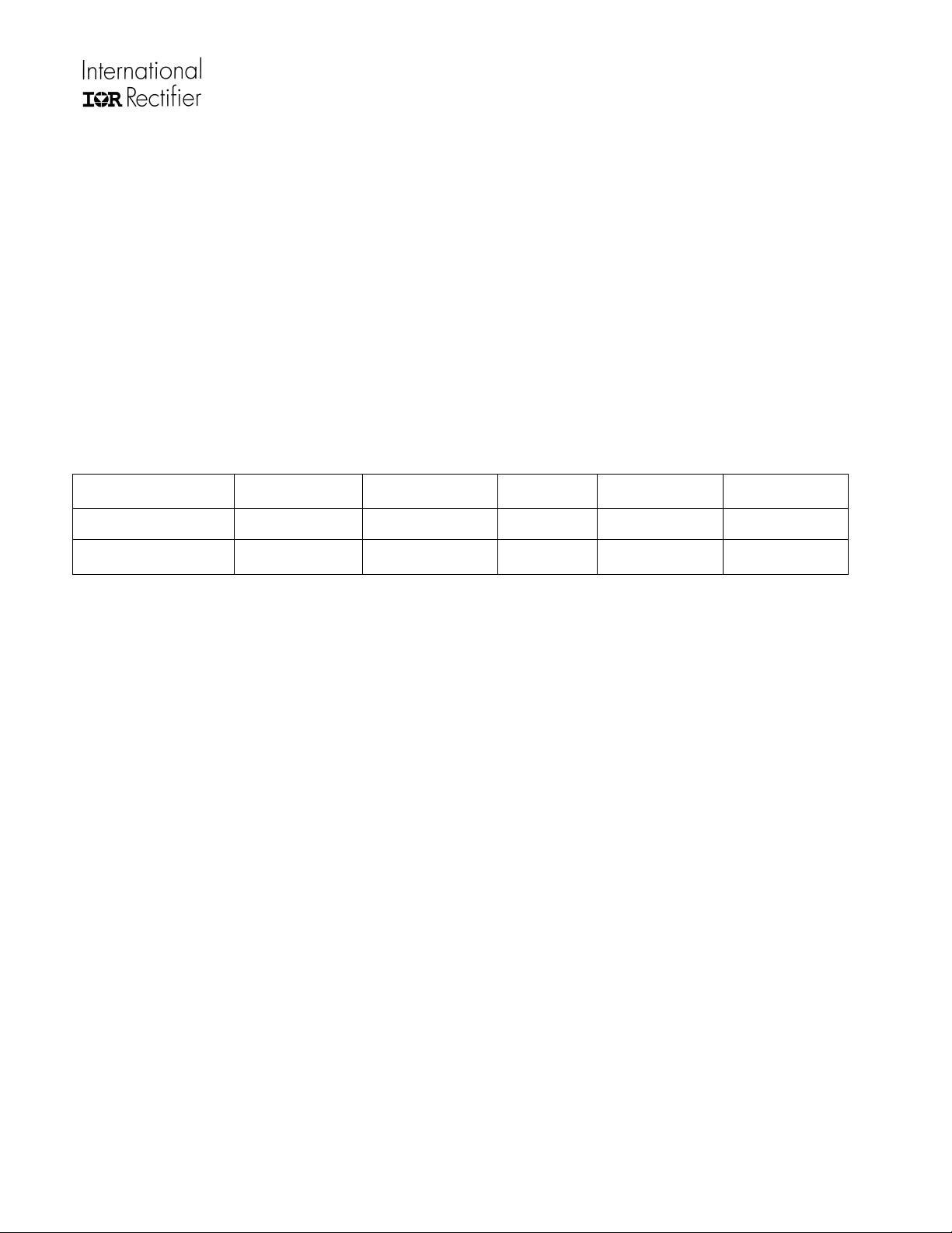
Typical Connection Diagram
www.irf.com © 2008 International Rectifier
HIGH VOLTAGE 3 PHASE GATE DRIVER IC
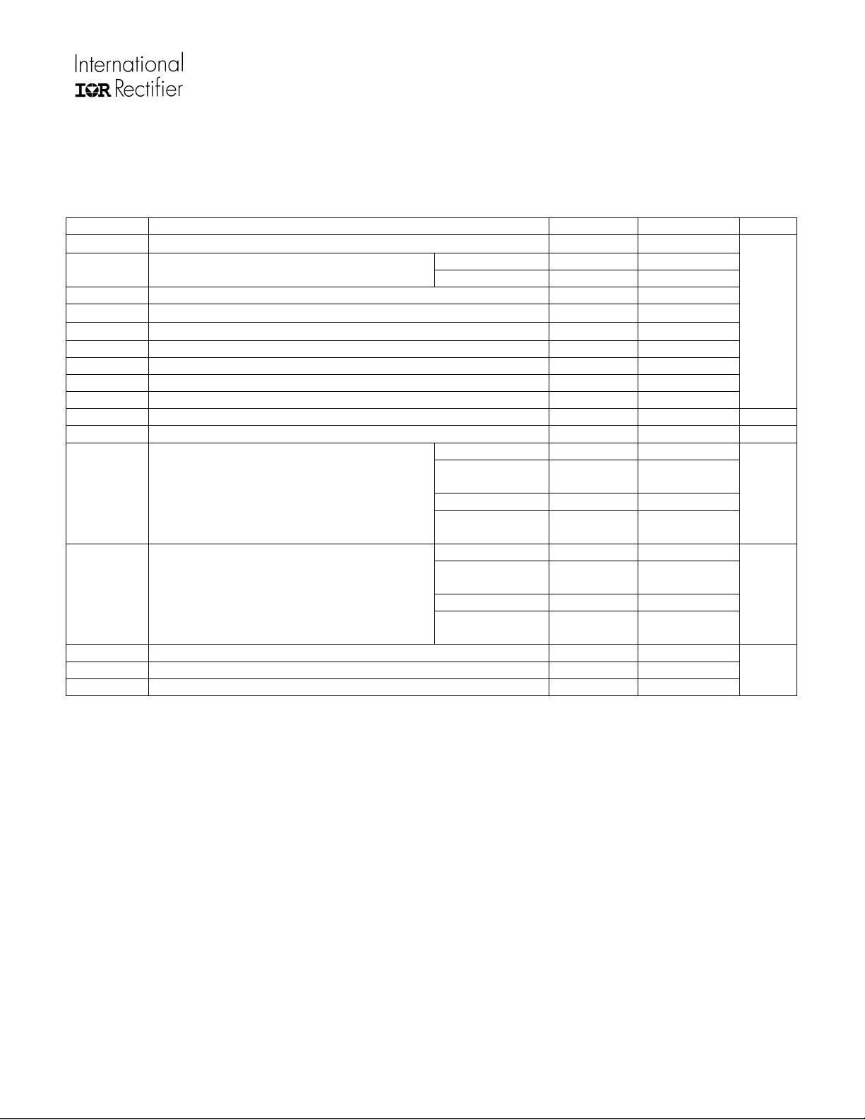
Product Summary
Topology 3 Phase
V
V
Io+ & I
tON & t
Deadtime (typical) 275 ns
≤ 600 V
OFFSET
IRS2336(D) 10 V – 20 V
IRS23364D 11.5 V – 20 V
(typical) 200 mA & 350 mA
o-
(typical) 530 ns & 530 ns
OFF
OUT
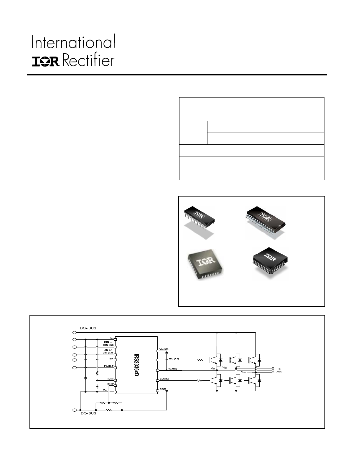
Package Options
28-Lead PDIP 28-Lead SOIC Wide Body
48-Lead MLPQ7X7 44-Lead PLCC
(without 14 leads) (without 12 leads)
IRS23364D

IRS2336x(D) Family
Table of Contents Page
Description 3
Feature Comparison 3
Simplified Block Diagram 4
Typical Application Diagram 4
Qualification Information 5
Absolute Maximum Ratings 6
Recommended Operating Conditions 7
Static Electrical Characteristics 8-9
Dynamic Electrical Characteristics 10
Functional Block Diagram 11-12
Input/Output Pin Equivalent Circuit Diagram 13-14
Lead Definitions 15-16
Lead Assignments 17
Application Information and Additional Details 18-34
Parameter Temperature Trends 35-38
Package Details 39-42
Tape and Reel Details 43-45
Part Marking Information 46
Ordering Information 47
www.irf.com © 2008 International Rectifier
2
IRS2336x(D) Family
Description
The IRS2336xD are high voltage, high speed, power MOSFET and IGBT gate drivers with three high-side and
three low-side referenced output channels for 3-phase applications. This IC is designed to be used with low-cost
bootstrap power supplies; the bootstrap diode functionality has been integrated into this device to reduce the
component count and the PCB size. Proprietary HVIC and latch immune CMOS technologies have been
implemented in a rugged monolithic structure. The floating logic input is compatible with standard CMOS or
LSTTL outputs (down to 3.3 V logic). A current trip function which terminates all six outputs can be derived from
an external current sense resistor. Enable functionality is available to terminate all six outputs simultaneously.
An open-drain FAULT signal is provided to indicate that a fault (e.g., over-current, over-temperature, or
undervoltage shutdown event) has occurred. Fault conditions are cleared automatically after a delay
programmed externally via an RC network connected to the RCIN input. The output drivers feature a high-pulse
current buffer stage designed for minimum driver cross-conduction. Shoot-through protection circuitry and a
minimum deadtime circuitry have been integrated into this IC. Propagation delays are matched to simplify the
HVIC’s use in high frequency applications. The floating channels can be used to drive N-channel power
MOSFETs or IGBTs in the high-side configuration, which operate up to 600 V.
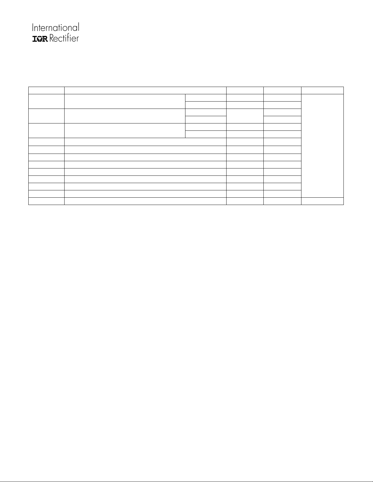
Feature Comparison: IRS2336xD Family
Part Number Input Logic UVLO V
IRS2336(D) HIN/N, LIN/N 8.9 V/ 8.2 V 0.46 V 530 ns, 530 ns 10 V – 20 V
IRS23364D HIN, LIN 11.1 V/ 10.9 V 0.46 V 530 ns, 530 ns 11.5 V – 20 V
t
IT,TH
ON
, t
V
OFF
OUT
www.irf.com © 2008 International Rectifier
3
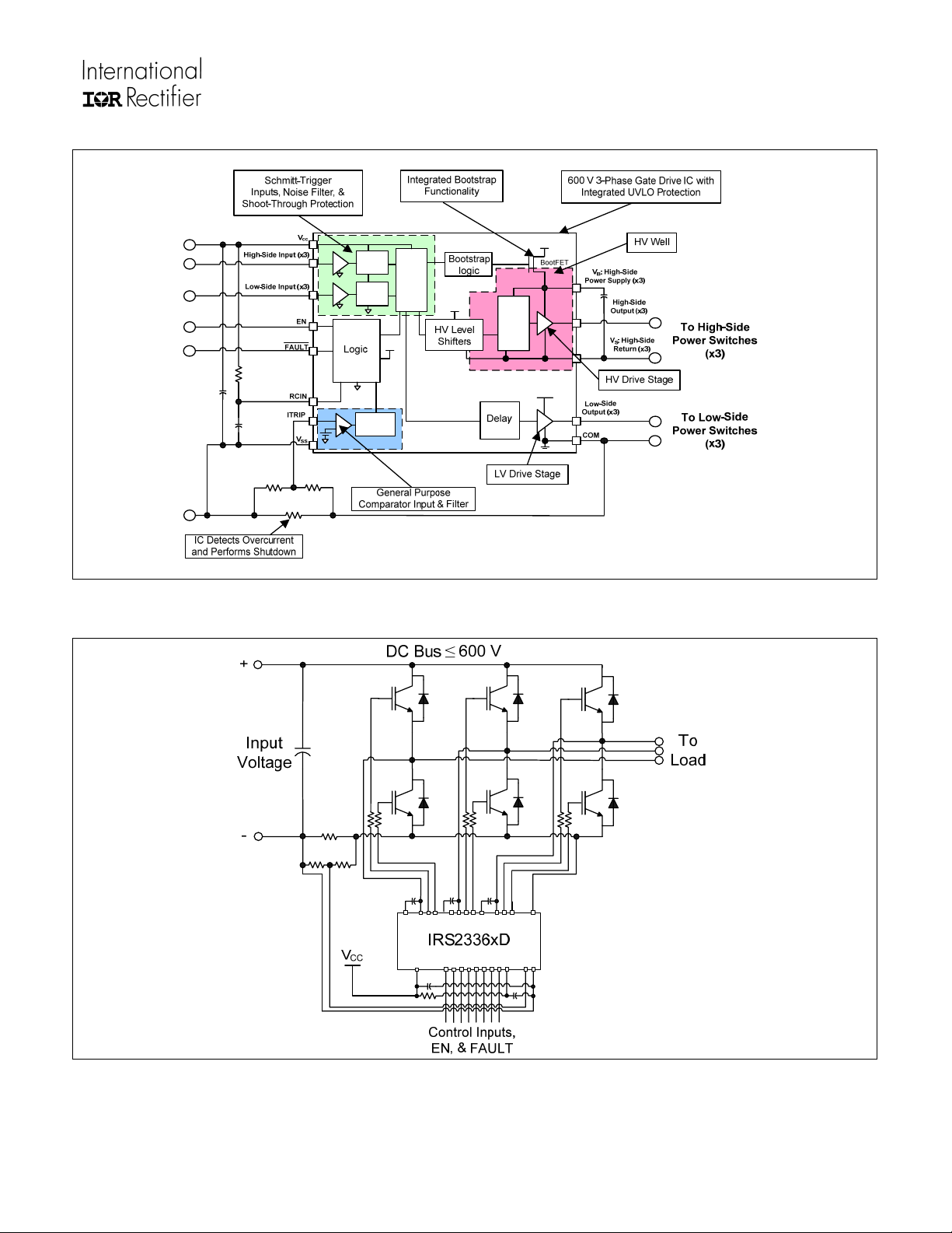
Simplified Block Diagram
IRS2336x(D) Family
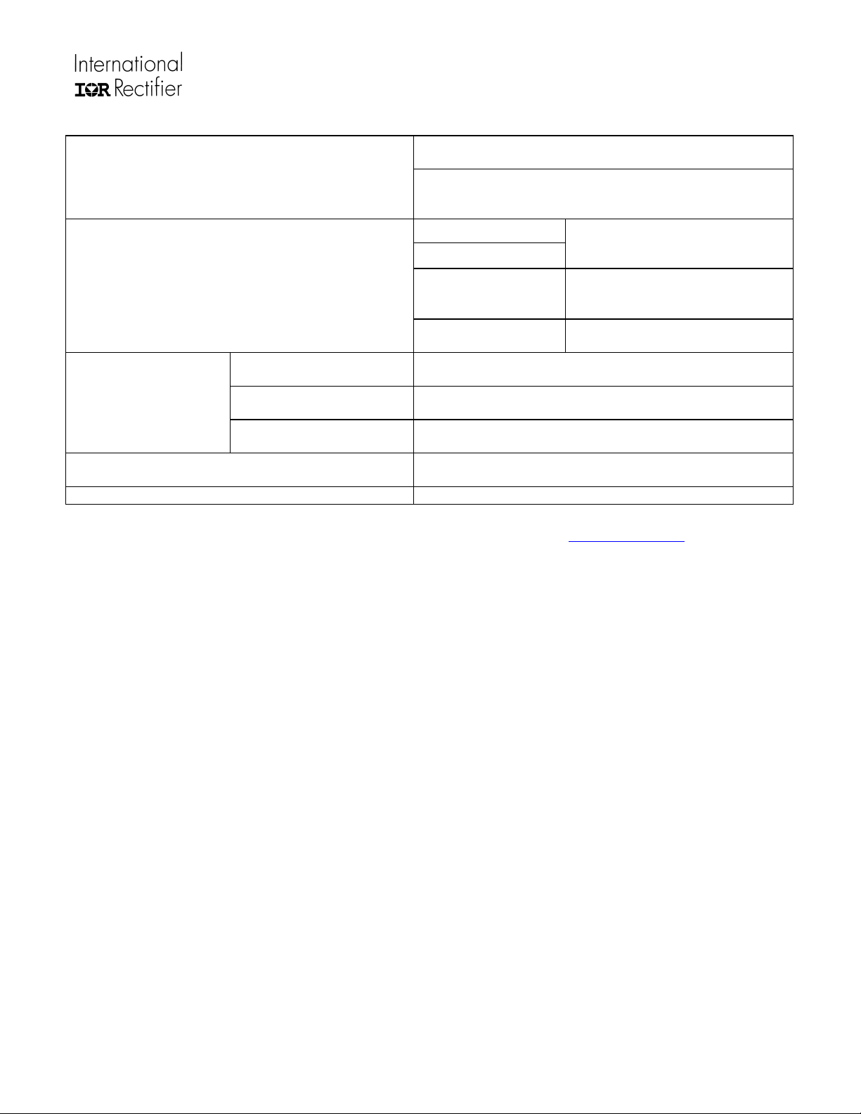
Typical Application Diagram
www.irf.com © 2008 International Rectifier
4
Qualification Information†
Qualification Level
Moisture Sensitivity Level
IRS2336x(D) Family
Industrial††
Comments: This family of ICs has passed JEDEC’s
Industrial qualification. IR’s Consumer qualification level is
granted by extension of the higher Industrial level.
SOIC28W
MLPQ7X7
PLCC44
(per IPC/JEDEC J-STD-020)
(per IPC/JEDEC J-STD-020)
MSL3
MSL3
†††
, 260°C
†††
, 245°C
Not applicable
ESD
IC Latch-Up Test
RoHS Compliant
PDIP28
Human Body Model
Machine Model
Charged Device Model
††††
(per JEDEC standard JESD22-A114)
(per EIA/JEDEC standard EIA/JESD22-A115)
(per JEDEC standard JESD22-C101)
(non-surface mount package style)
Class 2
Class B
Class IV
Class I, Level A
(per JESD78)
Yes
†
††
††† Higher MSL ratings may be available for the specific package types listed here. Please contact your
†††† Charged Device Model classification is based on SOIC28W package.
Qualification standards can be found at International Rectifier’s web site http://www.irf.com/
Higher qualification ratings may be available should the user have such requirements. Please contact your
International Rectifier sales representative for further information.
International Rectifier sales representative for further information.
www.irf.com © 2008 International Rectifier
5
IRS2336x(D) Family
V
ns
W
ºC
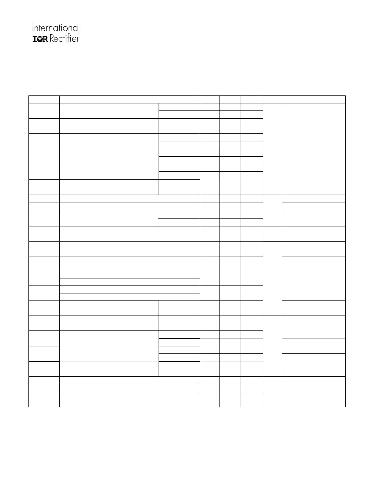
Absolute Maximum Ratings
Absolute maximum ratings indicate sustained limits beyond which damage to the device may occur. All voltage
parameters are absolute voltages referenced to V
unless otherwise stated in the table. The thermal resistance
SS
and power dissipation ratings are measured under board mounted and still air conditions. Voltage clamps are
included between V
& COM (25 V), VCC & VSS (20 V), and VB & VS (20 V).
CC
Symbol Definition Min Max Units
V
CC
V
IN
V
RCIN
V
B
VS High-side floating well supply return voltage
Low side supply voltage -0.3
Logic input voltage (HIN, LIN, ITRIP, EN)
IRS2336(D) VSS-0.3 VSS+5.2
IRS23364D V
-0.3 VCC+0.3
SS
RCIN input voltage VSS-0.3 VCC+0.3
High-side floating well supply voltage -0.3
-20†
V
B
620
V
20
+0.3
B
†
†
VHO Floating gate drive output voltage VS-0.3 VB+0.3
VLO Low-side output voltage COM-0.3 VCC+0.3
V
Fault output voltage VSS-0.3 VCC+0.3
FLT
COM Power ground VCC-25 VCC+0.3
dVS/dt Allowable VS offset supply transient relative to VSS
PW
High-side input pulse width 500
HIN
28-Lead PDIP
28-Lead
PD
Package power dissipation @ T
≤+25ºC
A
SOICW
44-Lead PLCC
48-Lead
MLPQ7X7
28-Lead PDIP
28-Lead
Rth
Thermal resistance, junction to ambient
JA
SOICW
44-Lead PLCC
48-Lead
MLPQ7X7
T
J
T
S
T
L
Junction temperature
Storage temperature -55 150
Lead temperature (soldering, 10 seconds)
—
—
— 1.6
—
— 2.0
—
— 78
—
—
—
—
50 V/ns
—
1.5
2.0
83
63
ºC/W
63
150
300
† All supplies are tested at 25 V. An internal 20 V clamp exists for each supply.
www.irf.com © 2008 International Rectifier
6
IRS2336x(D) Family
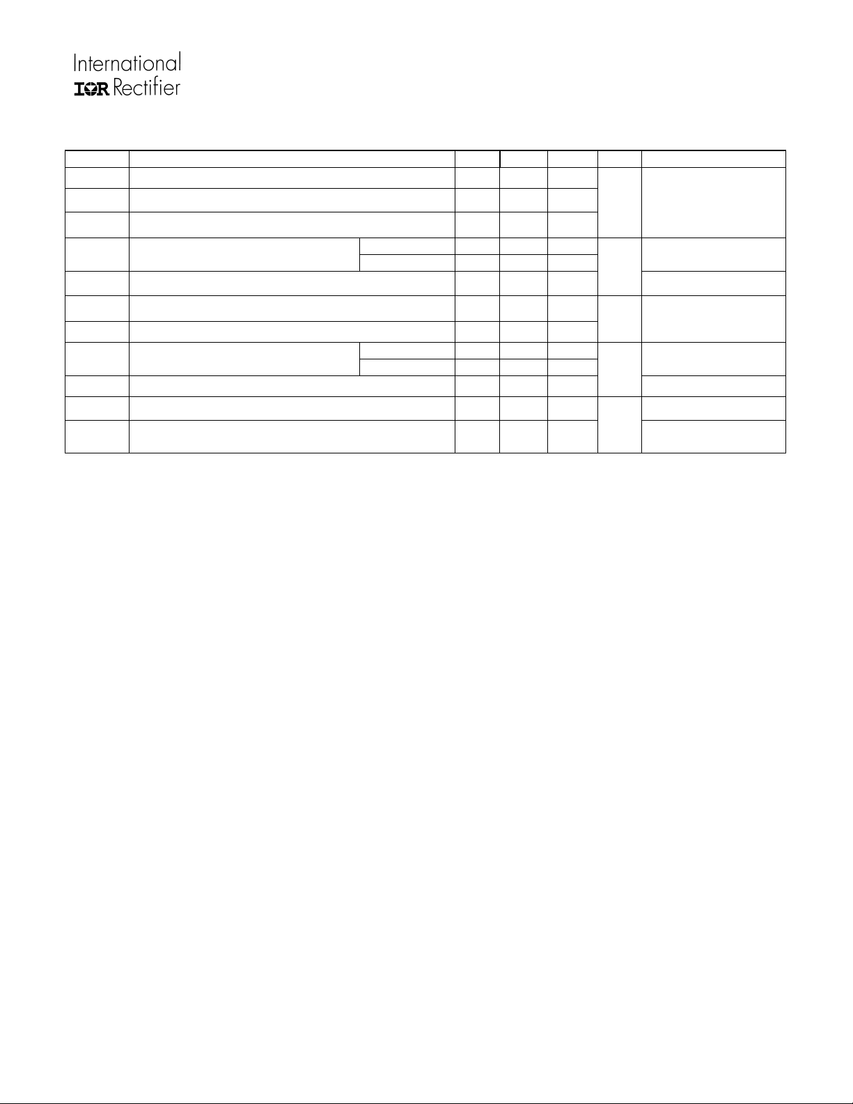
Recommended Operating Conditions
For proper operation, the device should be used within the recommended conditions. All voltage parameters are
absolute voltages referenced to V
(V
-COM) = (VB-VS) = 15 V.
CC
Symbol Definition Min Max Units
V
CC
V
IN
V
B
VS
VS(t)
Low-side supply voltage
HIN, LIN, & EN input voltage
High-side floating well supply voltage
High-side floating well supply offset voltage
Transient high-side floating supply voltage
VHO Floating gate drive output voltage Vs V
VLO Low-side output voltage COM VCC
COM Power ground -5 5
V
FAULT output voltage VSS V
FLT
V
RCIN input voltage VSS V
RCIN
V
ITRIP input voltage VSS V
ITRIP
T
A
Ambient temperature -40 125 ºC
†
Logic operation for
V
of –8 V to 600 V. Logic state held for
S
DT97-3 for more details.
†† Operational for transient negative V
the Application Information section of this datasheet for more details.
unless otherwise stated in the table. The offset rating is tested with supplies of
SS
IRS2336(D) 10 20
IRS23364D 11.5 20
IRS2336(D) VSS+5
IRS23364D
VSS
V
CC
IRS2336(D) VS+10 VS+20
IRS23364D V
†
††
V
of –8 V to –VBS. Please refer to Design Tip
S
of VSS - 50 V with a 50 ns pulse width. Guaranteed by design. Refer to
S
+11.5 VS+20
S
COM-8 600
-50 600
B
CC
CC
+5
SS
V
www.irf.com © 2008 International Rectifier
7
IRS2336x(D) Family
V
BSUV
Static Electrical Characteristics
(VCC-COM) = (VB-VS) = 15 V. TA = 25oC unless otherwise specified. The VIN and IIN parameters are referenced to
V
and are applicable to all six channels. The VO and IO parameters are referenced to respective VS and COM and
SS
are applicable to the respective output leads HO or LO.
parameters are referenced to V
.
S
Symbol Definition Min Typ Max Units Test Conditions
supply undervoltage positive
V
V
CCUV
V
CCUV
V
CCUVHY
V
BSUV+
V
BSUV-
V
BSUVHY
ILK
I
QBS
I
QCC
CC
+
going threshold
supply undervoltage negative
V
CC
-
going threshold
supply undervoltage
V
CC
hysteresis
V
BS
going threshold
V
BS
going threshold
supply undervoltage
V
BS
hysteresis
supply undervoltage positive
supply undervoltage negative
High-side floating well offset supply leakage
Quiescent V
Quiescent V
supply current
BS
supply current
CC
VOH High level output voltage drop, V
IRS2336(D) 8 8.9 9.8
IRS23364D 10.4 11.1 11.6
IRS2336(D) 7.4 8.2 9
IRS23364D 10.2 10.9 11.4
IRS2336(D) 0.3 0.7
IRS23364D
IRS2336(D) 8 8.9 9.8
IRS23364D 10.4 11.1 11.6
IRS2336(D) 7.4 8.2 9
IRS23364D 10.2 10.9 11.4
IRS2336(D) 0.3 0.7
IRS23364D
IRS2336
IR2336(4)D
BIAS-VO
VOL Low level output voltage drop, VO
I
Output high short circuit pulsed current 120 200 —
o+
I
Output low short circuit pulsed current 250 350 —
o-
VIH
V
IN,CLAMP
I
HIN+
I
HIN-
I
LIN+
I
LIN-
V
RCIN,TH
V
RCIN,HY
I
RCIN
R
ON,RCIN
VIL
Logic “0” input voltage
Logic “1” input voltage
Logic “1” input voltage
Logic “0” input voltage
Input voltage clamp
(HIN, LIN, ITRIP and EN)
Input bias current (HO = High)
Input bias current (HO = Low)
Input bias current (LO = High)
Input bias current (LO = Low)
RCIN positive going threshold
RCIN hysteresis
RCIN input bias current
RCIN low on resistance
IRS2336(D) 4.8 5.2 5.65
IRS2336(D)
IRS23364D
IRS2336(D)
IRS23364D
IRS2336(D)
IRS23364D
IRS2336(D)
IRS23364D
The
parameters are referenced to VSS. The
V
CCUV
—
—
0.2
—
V NA
—
—
— —
—
—
—
—
—
2.5
—
—
—
—
— —
—
—
—
—
—
—
— —
—
0.2
70 120
2 3
3 4
—
50 V
µA
All inputs are in the
mA
B
0.90 1.4 V
0.40 0.6 V
V
mA
—
—
—
0.8
V
O
=15 V,VIN=5 V,
V
O
150 200 VIN = 0 V
120 165
110 150
150 200
120 165
1
µA
110 150
—
8
3
50 100 Ω
1
—
—
1 µA V
V
RCIN
= VS = 600 V
off state
I
= 20 mA
O
=0 V,VIN=0 V,
PW ≤ 10 µs
PW ≤ 10 µs
NA
I
= 100 µA
IN
V
= 4 V
IN
V
= 0 V
IN
V
= 4 V
IN
= 0 V
V
IN
NA
= 0 V or 15 V
I = 1.5 mA
www.irf.com © 2008 International Rectifier
8
IRS2336x(D) Family
Static Electrical Characteristics (continued)
Symbol Definition Min Typ Max Units Test Conditions
V
ITRIP positive going threshold 0.37 0.46 0.55
IT,TH+
V
ITRIP negative going threshold
IT,TH-
V
ITRIP hysteresis
IT,HYS
I
“High” ITRIP input bias current
ITRIP+
I
“Low” ITRIP input bias current
ITRIP-
V
Enable positive going threshold
EN,TH+
V
Enable negative going threshold 0.8
EN,TH-
I
“High” enable input bias current
EN+
I
“Low” enable input bias current
EN-
R
FAULT low on resistance
ON,FLT
RBS
Internal BS diode Ron
(IRS2336(4)D)
IRS2336(D)
IRS23364D
IRS2336(D)
IRS23364D
—
—
—
—
0.4
0.07
5 20
5 40
— —
— —
—
—
—
5 20
120 165
— —
—
—
50 100 I = 1.5 mA
200 —
—
—
1
2.5
—
1
V
µA
V
µA
Ω
NA
VIN = 4 V
VIN = 0 V
NA
VIN = 4 V
VIN = 0 V
NA
www.irf.com © 2008 International Rectifier
9
IRS2336x(D) Family
Dynamic Electrical Characteristics
VCC= VB = 15 V, VS = VSS = COM, TA = 25oC, and CL = 1000 pF unless otherwise specified.
Symbol Definition Min Typ Max Units Test Conditions
t
ON
t
OFF
t
t
t
FIL,IN
tEN
t
FILTER,EN
t
FLTCLR
t
ITRIP
tBL ITRIP blanking time
t
FLT
DT Deadtime 190 275 420
MDT
MT
PM
† The minimum width of the input pulse is recommended to exceed 500 ns to ensure the filtering time of the
†† This parameter applies to all of the channels. Please see the application section for more details.
††† PM is defined as PW
Turn-on propagation delay 400 530 750
Turn-off propagation delay 400 530 750
Turn-on rise time
R
Turn-off fall time
F
Input filter time
(HIN, LIN, ITRIP)
†
Enable low to output shutdown
propagation delay
—
—
200 350 510
350 460 650 V
125 190
50 75
Enable input filter time 100 200
FAULT clear time
RCIN: R = 2 MΩ, C = 1 nF
ITRIP to output shutdown
propagation delay
1.3 1.65 2 ms
500 750 1200 V
—
400
ITRIP to FAULT propagation delay 400 600 950
††
DT matching
Delay matching time (t
Pulse width distortion
†††
ON
††
, t
)
OFF
— —
— — 50
— —
input filter is exceeded.
- PW
IN
OUT
.
—
—
60
75
ns
ns
= 0 V & 5 V
V
IN
= 0 V or 5 V
IN, VEN
NA
= 0 V or 5 V
V
IN
V
= 0 V
ITRIP
= 5 V
ITRIP
= 0 V or 5 V
V
IN
V
= 5 V
ITRIP
= 0 V & 5 V without
V
IN
external deadtime
V
= 0 V & 5 V with external
IN
deadtime larger than DT
PW input=10 µs
www.irf.com © 2008 International Rectifier
10
Functional Block Diagram: IRS2336(D)
IRS2336x(D) Family
Note: IRS2336 is without the “Integrated BootFET”
www.irf.com © 2008 International Rectifier
11
Functional Block Diagram: IRS23364D
IRS2336x(D) Family
www.irf.com © 2008 International Rectifier
12
Input/Output Pin Equivalent Circuit
IRS2336x(D) Family
Diagrams: IRS2336(D)
V
CC
ITRIP
or EN
V
SS
ESD
Diode
ESD
Diode
R
PD
www.irf.com © 2008 International Rectifier
13
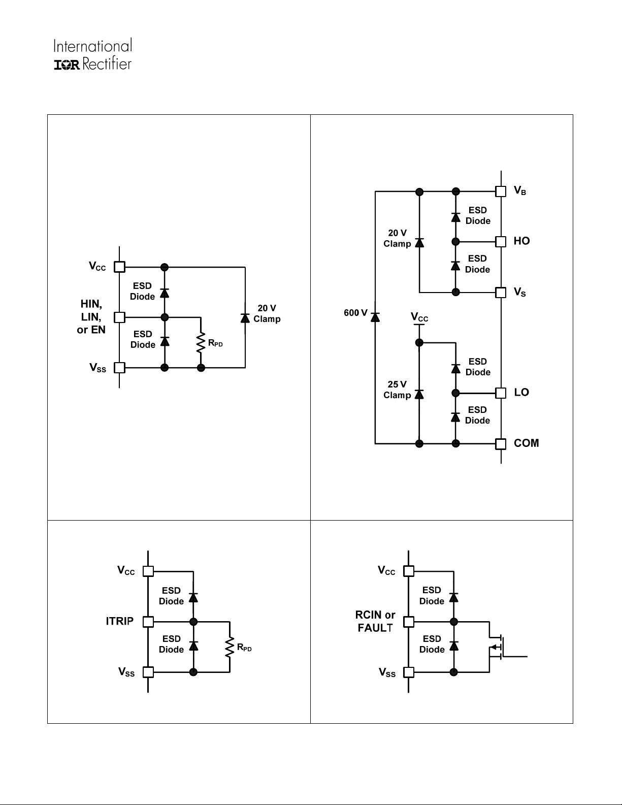
Input/Output Pin Equivalent Circuit
IRS2336x(D) Family
Diagrams: IRS23364D
www.irf.com © 2008 International Rectifier
14
IRS2336x(D) Family
Lead Definitions: IRS2336(D)
Symbol Description
VCC Low-side supply voltage
VSS Logic ground
VB1 High-side gate drive floating supply (phase 1)
VB2 High-side gate drive floating supply (phase 2)
VB3 High-side gate drive floating supply (phase 3)
VS1 High voltage floating supply return (phase 1)
VS2 High voltage floating supply return (phase 2)
VS3 High voltage floating supply return (phase 3)
HIN1/N Logic inputs for high-side gate driver outputs (phase 1); input is out-of-phase with output
HIN2/N Logic inputs for high-side gate driver outputs (phase 2); input is out-of-phase with output
HIN3/N Logic inputs for high-side gate driver outputs (phase 3); input is out-of-phase with output
LIN1/N Logic inputs for low-side gate driver outputs (phase 1); input is out-of-phase with output
LIN2/N Logic inputs for low-side gate driver outputs (phase 2); input is out-of-phase with output
LIN3/N Logic inputs for low-side gate driver outputs (phase 3); input is out-of-phase with output
HO1 High-side driver outputs (phase 1)
HO2 High-side driver outputs (phase 2)
HO3 High-side driver outputs (phase 3)
LO1 Low-side driver outputs (phase 1)
LO2 Low-side driver outputs (phase 2)
LO3 Low-side driver outputs (phase 3)
COM Low-side gate drive return
FAULT/N
EN
ITRIP
RCIN
Indicates over-current, over-temperature (ITRIP), or low-side undervoltage lockout has occurred.
This pin has negative logic and an open-drain output. The use of over-current and over-
temperature protection requires the use of external components.
Logic input to shutdown functionality. Logic functions when EN is high (i.e., positive logic). No
effect on FAULT and not latched.
Analog input for over-current shutdown. When active, ITRIP shuts down outputs and activates
FAULT and RCIN low. When ITRIP becomes inactive, FAULT stays active low for an externally
set time t
An external RC network input used to define the FAULT CLEAR delay (t
equal to R*C. When RCIN > 8 V, the FAULT pin goes back into an open-drain high-impedance
state.
, then automatically becomes inactive (open-drain high impedance).
FLTCLR
approximately
FLTCLR)
www.irf.com © 2008 International Rectifier
15

IRS2336x(D) Family
Lead Definitions: IRS23364D
Symbol Description
VCC Low-side supply voltage
VSS Logic ground
VB1 High-side gate drive floating supply (phase 1)
VB2 High-side gate drive floating supply (phase 2)
VB3 High-side gate drive floating supply (phase 3)
VS1 High voltage floating supply return (phase 1)
VS2 High voltage floating supply return (phase 2)
VS3 High voltage floating supply return (phase 3)
HIN1 Logic inputs for high-side gate driver outputs (phase 1); input is in-phase with output
HIN2 Logic inputs for high-side gate driver outputs (phase 2); input is in-phase with output
HIN3 Logic inputs for high-side gate driver outputs (phase 3); input is in-phase with output
LIN1 Logic inputs for low-side gate driver outputs (phase 1); input is in-phase with output
LIN2 Logic inputs for low-side gate driver outputs (phase 2); input is in-phase with output
LIN3 Logic inputs for low-side gate driver outputs (phase 3); input is in-phase with output
HO1 High-side driver outputs (phase 1)
HO2 High-side driver outputs (phase 2)
HO3 High-side driver outputs (phase 3)
LO1 Low-side driver outputs (phase 1)
LO2 Low-side driver outputs (phase 2)
LO3 Low-side driver outputs (phase 3)
COM Low-side gate drive return
FAULT/N
EN
ITRIP
RCIN
Indicates over-current, over-temperature (ITRIP), or low-side undervoltage lockout has occurred.
This pin has negative logic and an open-drain output. The use of over-current and over-
temperature protection requires the use of external components.
Logic input to shutdown functionality. Logic functions when EN is high (i.e., positive logic). No
effect on FAULT and not latched.
Analog input for over-current shutdown. When active, ITRIP shuts down outputs and activates
FAULT and RCIN low. When ITRIP becomes inactive, FAULT stays active low for an externally
set time t
An external RC network input used to define the FAULT CLEAR delay (t
equal to R*C. When RCIN > 8 V, the FAULT pin goes back into an open-drain high-impedance
state.
, then automatically becomes inactive (open-drain high impedance).
FLTCLR
approximately
FLTCLR)
www.irf.com © 2008 International Rectifier
16

)
Lead Assignments
IRS2336x(D) Family
IRS2336(D
www.irf.com © 2008 International Rectifier
17

IRS2336x(D) Family
Application Information and Additional Details
Information regarding the following topics are included as subsections within this section of the datasheet.
• IGBT/MOSFET Gate Drive
• Switching and Timing Relationships
• Deadtime
• Matched Propagation Delays
• Input Logic Compatibility
• Undervoltage Lockout Protection
• Shoot-Through Protection
• Enable Input
• Fault Reporting and Programmable Fault Clear Timer
• Over-Current Protection
• Over-Temperature Shutdown Protection
• Truth Table: Undervoltage lockout, ITRIP, and ENABLE
• Advanced Input Filter
• Short-Pulse / Noise Rejection
• Integrated Bootstrap Functionality
• Bootstrap Power Supply Design
• Separate Logic and Power Grounds
• Tolerant to Negative V
• PCB Layout Tips
• Additional Documentation
IGBT/MOSFET Gate Drive
The IRS2336xD HVICs are designed to drive up to six MOSFET or IGBT power devices. Figures 1 and 2 illustrate
several parameters associated with the gate drive functionality of the HVIC. The output current of the HVIC, used to
drive the gate of the power switch, is defined as I
defined as V
generically called V
Transients
S
. The voltage that drives the gate of the external power switch is
O
for the high-side power switch and VLO for the low-side power switch; this parameter is sometimes
HO
and in this case does not differentiate between the high-side or low-side output voltage.
OUT
V
B
(or VCC)
HO
(or LO)
V
S
(or COM)
+
V
HO
-
I
(or VLO)
O+
V
B
(or VCC)
HO
(or LO)
V
S
(or COM)
I
O-
Figure 1: HVIC sourcing current Figure 2: HVIC sinking current
www.irf.com © 2008 International Rectifier
18

IRS2336x(D) Family
Switching and Timing Relationships
The relationship between the input and output signals of the IRS2336(D) and IRS23364D are illustrated below in
Figures 3 and 4. From these figures, we can see the definitions of several timing parameters (i.e., PW
t
, tR, and tF) associated with this device.
OFF
Figure 3: Switching time waveforms (IRS2336(D)) Figure 4: Switching time waveforms (IRS23364D)
The following two figures illustrate the timing relationships of some of the functionality of the IRS2336xD; this
functionality is described in further detail later in this document.
During interval A of Figure 5, the HVIC has received the command to turn-on both the high- and low-side switches at
the same time; as a result, the shoot-through protection of the HVIC has prevented this condition and both the highand low-side output are held in the off state.
Interval B of Figures 5 and 6 shows that the signal on the ITRIP input pin has gone from a low to a high state; as a
result, all of the gate drive outputs have been disabled (i.e., see that HOx has returned to the low state; LOx is also
held low), the voltage on the RCIN pin has been pulled to 0 V, and a fault is reported by the FAULT output
transitioning to the low state. Once the ITRIP input has returned to the low state, the output will remain disabled and
the fault condition reported until the voltage on the RCIN pin charges up to V
charging characteristics are dictated by the RC network attached to the RCIN pin.
During intervals D and E of Figure 5, we can see that the enable (EN) pin has been pulled low (as is the case when
the driver IC has received a command from the control IC to shutdown); this results in the outputs (HOx and LOx)
being held in the low state until the enable pin is pulled high.
, PW
IN
OUT
, tON,
(see interval C in Figure 6); the
RCIN,TH
www.irf.com © 2008 International Rectifier
19

IRS2336x(D) Family
Figure 5: Input/output timing diagram for the IRS2336xD family
Figure 6: Detailed view of B & C intervals
Deadtime
This family of HVICs features integrated deadtime protection circuitry. The deadtime for these ICs is fixed; other ICs
within IR’s HVIC portfolio feature programmable deadtime for greater design flexibility. The deadtime feature inserts
a time period (a minimum deadtime) in which both the high- and low-side power switches are held off; this is done to
ensure that the power switch being turned off has fully turned off before the second power switch is turned on. This
minimum deadtime is automatically inserted whenever the external deadtime is shorter than DT; external deadtimes
larger than DT are not modified by the gate driver. Figure 7 illustrates the deadtime period and the relationship
between the output gate signals.
The deadtime circuitry of the IRS2336xD is matched with respect to the high- and low-side outputs of a given
channel; additionally, the deadtimes of each of the three channels are matched. Figure 7 defines the two deadtime
parameters (i.e., DT
IRS2336xD specifies the maximum difference between DT
comparing the DT of one channel of the IRS2336xD to that of another.
www.irf.com © 2008 International Rectifier
and DT2) of a specific channel; the deadtime matching parameter (MDT) associated with the
1
and DT2. The MDT parameter also applies when
1
20

IRS2336x(D) Family
LINx
HINx
LOx
HOx
50%
50%
50%
DTDT
50%
Figure 7: Illustration of deadtime
Matched Propagation Delays
The IRS2336xD family of HVICs is designed with propagation delay matching circuitry. With this feature, the IC’s
, t
response at the output to a signal at the input requires approximately the same time duration (i.e., t
ON
) for both
OFF
the low-side channels and the high-side channels; the maximum difference is specified by the delay matching
parameter (MT). Additionally, the propagation delay for each low-side channel is matched when compared to the
other low-side channels and the propagation delays of the high-side channels are matched with each other; the MT
specification applies as well. The propagation turn-on delay (t
turn-on delay (t
OFF
).
) of the IRS2336xD is matched to the propagation
ON
Input Logic Compatibility
The inputs of this IC are compatible with standard CMOS and TTL outputs. The IRS2336xD family has been
designed to be compatible with 3.3 V and 5 V logic-level signals. The IRS2336(D) features an integrated 5.2 V
Zener clamp on the HIN, LIN, ITRIP, and EN pins; the IRS23364D does not offer this input clamp. Figure 8
illustrates an input signal to the IRS2336(D) and IRS23364D, its input threshold values, and the logic state of the IC
as a result of the input signal.
Figure 8: HIN & LIN input thresholds
www.irf.com © 2008 International Rectifier
21

IRS2336x(D) Family
Undervoltage Lockout Protection
This family of ICs provides undervoltage lockout protection on both the V
supply and the V
plotted over time and as the waveform crosses the UVLO threshold (V
is enabled or disabled.
Upon power-up, should the V
V
voltage decreases below the V
CC
a fault condition and shutdown the high- and low-side gate drive outputs, and the FAULT pin will transition to the low
state to inform the controller of the fault condition.
Upon power-up, should the V
voltage decreases below the V
V
BS
fault condition, and shutdown the high-side gate drive outputs of the IC.
The UVLO protection ensures that the IC drives the external power devices only when the gate supply voltage is
sufficient to fully enhance the power devices. Without this feature, the gates of the external power switch could be
driven with a low voltage, resulting in the power switch conducting current while the channel impedance is high; this
could result in very high conduction losses within the power device and could lead to power device failure.
(logic and low-side circuitry) power
CC
(high-side circuitry) power supply. Figure 9 is used to illustrate this concept; VCC (or VBS) is
BS
voltage fail to reach the V
CC
threshold during operation, the undervoltage lockout circuitry will recognize
CCUV-
voltage fail to reach the V
BS
threshold during operation, the undervoltage lockout circuitry will recognize a
BSUV
or V
CCUV+/-
threshold, the IC will not turn-on. Additionally, if the
CCUV+
threshold, the IC will not turn-on. Additionally, if the
BSUV
) the undervoltage protection
BSUV+/-
Figure 9: UVLO protection
Shoot-Through Protection
The IRS2336xD family of high-voltage ICs is equipped with shoot-through protection circuitry (also known as crossconduction prevention circuitry). Figure 10 shows how this protection circuitry prevents both the high- and low-side
switches from conducting at the same time. Table 1 illustrates the input/output relationship of the devices in the form
of a truth table. Note that the IRS2336(D) has inverting inputs (the output is out-of-phase with its respective input)
while the IRS23364D has non-inverting inputs (the output is in-phase with its respective input).
www.irf.com © 2008 International Rectifier
22

IRS2336x(D) Family
Shoot-through
protection enabled
HIN
LIN
HO
LO
Figure 10: Illustration of shoot-through protection circuitry
IRS2336(D) IRS23364D
HIN LIN HO LO HIN LIN HO LO
0 0 0 0 0 0 0 0
0 1 1 0 0 1 0 1
1 0 0 1 1 0 1 0
1 1 0 0
1 1 0 0
Table 1: Input/output truth table for IRS2336D and IRS23364D
Enable Input
The IRS2336xD family of HVICs is equipped with an enable input pin that is used to shutdown or enable the HVIC.
When the EN pin is in the high state the HVIC is able to operate normally (assuming no other fault conditions).
When a condition occurs that should shutdown the HVIC, the EN pin should see a low logic state. The enable
circuitry of the IRS2336xD features an input filter; the minimum input duration is specified by t
to the EN pin parameters V
EN,TH+
, V
, and IEN for the details of its use. Table 2 gives a summary of this pin’s
EN,TH-
FILTER,EN
. Please refer
functionality and Figure 11 illustrates the outputs’ response to a shutdown command.
Enable Input
Enable input high Outputs enabled*
Enable input low Outputs disabled
Table 2: Enable functionality truth table
Figure 11: Output enable timing waveform
(*assumes no other fault condition)
www.irf.com © 2008 International Rectifier
23

IRS2336x(D) Family
Fault Reporting and Programmable Fault Clear Timer
The IRS2336xD family provides an integrated fault reporting output and an adjustable fault clear timer. There are
two situations that would cause the HVIC to report a fault via the FAULT pin. The first is an undervoltage condition
of V
and the second is if the ITRIP pin recognizes a fault. Once the fault condition occurs, the FAULT pin is
CC
internally pulled to V
condition has been removed and the fault clear timer expires; once the fault clear timer expires, the voltage on the
FAULT pin will return to V
The length of the fault clear time period (t
capacitor where the time constant is set by R
occurred (UVLO or ITRIP), RCIN and FAULT are pulled to V
timer begins. Figure 13 shows that R
between the RCIN and V
and the fault clear timer is activated. The fault output stays in the low state until the fault
SS
.
CC
) is determined by exponential charging characteristics of the
FLTCLR
pins.
SS
and C
RCIN
is connected between the VCC and the RCIN pin, while C
RCIN
. In Figure 12 where we see that a fault condition has
RCIN
, and once the fault has been removed, the fault clear
SS
is placed
RCIN
Figure 12: RCIN and FAULT pin waveforms Figure 13: Programming the fault clear timer
The design guidelines for this network are shown in Table 3.
≤1 nF
C
RCIN
Ceramic
0.5 MΩ to 2 MΩ
R
RCIN
>> R
ON,RCIN
Table 3: Design guidelines
The length of the fault clear time period can be determined by using the formula below.
(t) = Vf(1-e
v
C
-t/RC
)
t
FLTCLR
= -(R
RCINCRCIN
)ln(1-V
RCIN,TH/VCC
)
www.irf.com © 2008 International Rectifier
24

IRS2336x(D) Family
Over-Current Protection
The IRS2336xD HVICs are equipped with an ITRIP input pin. This functionality can be used to detect over-current
events in the DC- bus. Once the HVIC detects an over-current event through the ITRIP pin, the outputs are
shutdown, a fault is reported through the FAULT pin, and RCIN is pulled to V
The level of current at which the over-current protection is initiated is determined by the resistor network (i.e., R
and R
) connected to ITRIP as shown in Figure 14, and the ITRIP threshold (V
2
to determine the maximum allowable level of current in the DC- bus and select R
at node V
reaches the over-current threshold (V
X
.
SS
, R1,
0
). The circuit designer will need
IT,TH+
, R1, and R2 such that the voltage
0
) at that current level.
IT,TH+
V
IT,TH+
= R0I
DC-(R1
/(R1+R2))
Figure 14: Programming the over-current protection
For example, a typical value for resistor R
could be 50 mΩ. The voltage of the ITRIP pin should not be allowed to
0
exceed 5 V; if necessary, an external voltage clamp may be used.
Over-Temperature Shutdown Protection
The ITRIP input of the IRS2336xD can also be used to detect over-temperature events in the system and initiate a
shutdown of the HVIC (and power switches) at that time. In order to use this functionality, the circuit designer will
need to design the resistor network as shown in Figure 15 and select the maximum allowable temperature.
This network consists of a thermistor and two standard resistors R
resistance of the thermistor will change; this will result in a change of voltage at node V
be selected such the voltage V
should reach the threshold voltage (V
X
and R4. As the temperature changes, the
3
. The resistor values should
X
) of the ITRIP functionality by the time that
IT,TH+
the maximum allowable temperature is reached. The voltage of the ITRIP pin should not be allowed to exceed 5 V.
When using both the over-current protection and over-temperature protection with the ITRIP input, OR-ing diodes
(e.g., DL4148) can be used. This network is shown in Figure 16; the OR-ing diodes have been labeled D
and D2.
1
www.irf.com © 2008 International Rectifier
25

IRS2336x(D) Family
Figure 15: Programming over-temperature
protection
Figure 16: Using over-current protection and over-
temperature protection
Truth Table: Undervoltage lockout, ITRIP, and ENABLE
Table 4 provides the truth table for the IRS2336xD. The first line shows that the UVLO for V
FAULT output has gone low and the gate drive outputs have been disabled.
when V
is greater than
CC
, the FAULT output returns to the high impedance state.
V
CCUV
is not latched in this case and
V
CCUV
has been tripped; the
CC
The second case shows that the UVLO for V
disabled. After V
exceeds the
BS
V
BSUV
has been tripped and that the high-side gate drive outputs have been
BS
threshold
, HO will stay low until the HVIC input receives a new falling
(IRS2336(D)) or rising (IRS23364D) transition of HIN. The third case shows the normal operation of the HVIC. The
fourth case illustrates that the ITRIP trip threshold has been reached and that the gate drive outputs have been
disabled and a fault has been reported through the fault pin. In the last case, the HVIC has received a command
through the EN input to shutdown; as a result, the gate drive outputs have been disabled.
VCC VBS ITRIP EN RCIN FAULT LO HO
<
UVLO VCC
UVLO VBS
Normal operation
ITRIP fault
EN command
V
CCUV
15 V
— — —
<
V
BSUV
0 V 5 V High High impedance LIN 0
15 V 15 V 0 V 5 V High High impedance LIN HIN
15 V 15 V >V
15 V 15 V 0 V 0 V High High impedance 0 0
5 V Low 0 0 0
ITRIP
High 0 0 0
Table 4: IRS2336xD UVLO, ITRIP, EN, RCIN, & FAULT truth table
Advanced Input Filter
The advanced input filter allows an improvement in the input/output pulse symmetry of the HVIC and helps to reject
noise spikes and short pulses. This input filter has been applied to the HIN, LIN, and EN inputs. The working
principle of the new filter is shown in Figures 17 and 18.
Figure 17 shows a typical input filter and the asymmetry of the input and output. The upper pair of waveforms
(Example 1) show an input signal with a duration much longer then t
difference between the input signal and t
duration slightly longer then t
t
.
FIL,IN
; the resulting output is approximately the difference between the input signal and
FIL,IN
. The lower pair of waveforms (Example 2) show an input signal with a
FIL,IN
; the resulting output is approximately the
FIL,IN
Figure 18 shows the advanced input filter and the symmetry between the input and output. The upper pair of
waveforms (Example 1) show an input signal with a duration much longer then t
www.irf.com © 2008 International Rectifier
26
; the resulting output is
FIL,IN

IRS2336x(D) Family
approximately the same duration as the input signal. The lower pair of waveforms (Example 2) show an input signal
with a duration slightly longer then t
; the resulting output is approximately the same duration as the input signal.
FIL,IN
Figure 17: Typical input filter Figure 18: Advanced input filter
Short-Pulse / Noise Rejection
This device’s input filter provides protection against short-pulses (e.g., noise) on the input lines. If the duration of the
input signal is less than t
in the low state with positive noise spikes of durations less than t
of Figure 19 shows the input and output in the high state with negative noise spikes of durations less than t
, the output will not change states. Example 1 of Figure 19 shows the input and output
FIL,IN
; the output does not change states. Example 2
FIL,IN
FIL,IN
; the
output does not change states.
Example 1
Example 2
Figure 19: Noise rejecting input filters
Figures 20 and 21 present lab data that illustrates the characteristics of the input filters while receiving ON and OFF
pulses.
The input filter characteristic is shown in Figure 20; the left side illustrates the narrow pulse ON (short positive pulse)
characteristic while the left shows the narrow pulse OFF (short negative pulse) characteristic. The x-axis of Figure
20 shows the duration of PW
duration less than t
, that the resulting PW
FIL,IN
also see that once the PW
, while the y-axis shows the resulting PW
IN
duration is zero (e.g., the filter rejects the input signal/noise). We
OUT
duration exceed t
IN
, that the PW
FIL,IN
duration. It can be seen that for a PWIN
OUT
durations mimic the PWIN durations very well over
OUT
this interval with the symmetry improving as the duration increases. To ensure proper operation of the HVIC, it is
suggested that the input pulse width for the high-side inputs be ≥ 500 ns.
www.irf.com © 2008 International Rectifier
27

IRS2336x(D) Family
The difference between the PW
Figure 21; the careful reader will note the scale of the y-axis. The x-axis of Figure 21 shows the duration of PW
while the y-axis shows the resulting PW
of this input filter.
and PWIN signals of both the narrow ON and narrow OFF cases is shown in
OUT
–PWIN duration. This data illustrates the performance and near symmetry
OUT
,
IN
OUT
IN
Narrow Pulse OFF
Time (ns)
Time (ns)
1000
800
600
400
200
0
PW
PW
0 200 400 600 800 1000
Figure 20: IRS2336xD input filter characteristic
Figure 21: Difference between the input pulse and the output pulse
Integrated Bootstrap Functionality
The new IRS2336xD family features integrated high-voltage bootstrap MOSFETs that eliminate the need of the
external bootstrap diodes and resistors in many applications.
There is one bootstrap MOSFET for each high-side output channel and it is connected between the V
its respective floating supply (i.e., V
, VB2, VB3); see Figure 22 for an illustration of this internal connection.
B1
supply and
CC
The integrated bootstrap MOSFET is turned on only during the time when LO is ‘high’, and it has a limited source
current due to R
C
capacitor, the drain-source (collector-emitter) drop of the external IGBT (or MOSFET), and the low-side free-
BS
. The VBS voltage will be charged each cycle depending on the on-time of LO and the value of the
BS
wheeling diode drop.
The bootstrap MOSFET of each channel follows the state of the respective low-side output stage (i.e., the bootstrap
MOSFET is ON when LO is high, it is OFF when LO is low), unless the V
110% of V
. In that case, the bootstrap MOSFET is designed to remain off until VB returns below that threshold; this
CC
voltage is higher than approximately
B
concept is illustrated in Figure 23.
www.irf.com © 2008 International Rectifier
28

IRS2336x(D) Family
Figure 22: Internal bootstrap MOSFET connection Figure 23: Bootstrap MOSFET state diagram
A bootstrap MOSFET is suitable for most of the PWM modulation schemes and can be used either in parallel with
the external bootstrap network (i.e., diode and resistor) or as a replacement of it. The use of the integrated bootstrap
as a replacement of the external bootstrap network may have some limitations. An example of this limitation may
arise when this functionality is used in non-complementary PWM schemes (typically 6-step modulations) and at very
high PWM duty cycle. In these cases, superior performances can be achieved by using an external bootstrap diode
in parallel with the internal bootstrap network.
Bootstrap Power Supply Design
For information related to the design of the bootstrap power supply while using the integrated bootstrap functionality
of the IRS2336xD family, please refer to Application Note 1123 (AN-1123) entitled “Bootstrap Network Analysis:
Focusing on the Integrated Bootstrap Functionality.” This application note is available at www.irf.com
.
For information related to the design of a standard bootstrap power supply (i.e., using an external discrete diode)
please refer to Design Tip 04-4 (DT04-4) entitled “Using Monolithic High Voltage Gate Drivers.” This design tip is
available at www.irf.com
.
Separate Logic and Power Grounds
The IRS2336xD has separate logic and power ground pin (V
and COM respectively) to eliminate some of the noise
SS
problems that can occur in power conversion applications. Current sensing shunts are commonly used in many
applications for power inverter protection (i.e., over-current protection), and in the case of motor drive applications,
for motor current measurements. In these situations, it is often beneficial to separate the logic and power grounds.
Figure 24 shows a HVIC with separate V
V
is used as the reference point for the logic and over-current circuitry; VX in the figure is the voltage between the
SS
ITRIP pin and the V
pin. Alternatively, the COM pin is the reference point for the low-side gate drive circuitry. The
SS
output voltage used to drive the low-side gate is V
output voltage of the driver minus the drop across R
and COM pins and how these two grounds are used in the system. The
SS
-COM; the gate-emitter voltage (VGE) of the low-side switch is the
LO
.
G,LO
www.irf.com © 2008 International Rectifier
29

IRS2336x(D) Family
DC+ BUS
D
BS
V
V
CC
(x3)
HO
(x3)
B
C
BS
R
G,HO
HVIC
ITRIP
V
SS
Figure 24: Separate V
V
(x3)
LO
(x3)
COM
S
DC- BUS
V
S1
R
G,LO
+
V
GE1
-
R
2
+
R
1
V
X
-
V
S2
+
V
GE2
-
R
0
V
S3
+
V
GE3
-
and COM pins
SS
Tolerant to Negative V
Transients
S
A common problem in today’s high-power switching converters is the transient response of the switch node’s voltage
as the power switches transition on and off quickly while carrying a large current. A typical 3-phase inverter circuit is
shown in Figure 25; here we define the power switches and diodes of the inverter.
If the high-side switch (e.g., the IGBT Q1 in Figures 26 and 27) switches off, while the U phase current is flowing to
an inductive load, a current commutation occurs from high-side switch (Q1) to the diode (D2) in parallel with the lowside switch of the same inverter leg. At the same instance, the voltage node V
, swings from the positive DC bus
S1
voltage to the negative DC bus voltage.
Figure 25: Three phase inverter
www.irf.com © 2008 International Rectifier
30

IRS2336x(D) Family
DC+ BUS
Q1
ON
I
U
V
S1
DC- BUS
D2
Q2
OFF
Figure 26: Q1 conducting Figure 27: D2 conducting
Also when the V phase current flows from the inductive load back to the inverter (see Figures 28 and 29), and Q4
IGBT switches on, the current commutation occurs from D3 to Q4. At the same instance, the voltage node, V
,
S2
swings from the positive DC bus voltage to the negative DC bus voltage.
DC+ BUS
V
S2
DC- BUS
D3
D4
I
V
Q3
OFF
Q4
OFF
Figure 28: D3 conducting Figure 29: Q4 conducting
However, in a real inverter circuit, the V
swings below the level of the negative DC bus. This undershoot voltage is called “negative V
voltage swing does not stop at the level of the negative DC bus, rather it
S
transient”.
S
The circuit shown in Figure 30 depicts one leg of the three phase inverter; Figures 31 and 32 show a simplified
illustration of the commutation of the current between Q1 and D2. The parasitic inductances in the power circuit from
the die bonding to the PCB tracks are lumped together in L
V
is below the DC+ voltage by the voltage drops associated with the power switch and the parasitic elements of
S1
and LE for each IGBT. When the high-side switch is on,
C
the circuit. When the high-side power switch turns off, the load current momentarily flows in the low-side
freewheeling diode due to the inductive load connected to V
(the load is not shown in these figures). This current
S1
flows from the DC- bus (which is connected to the COM pin of the HVIC) to the load and a negative voltage between
and the DC- Bus is induced (i.e., the COM pin of the HVIC is at a higher potential than the VS pin).
V
S1
www.irf.com © 2008 International Rectifier
31

IRS2336x(D) Family
Figure 30: Parasitic Elements Figure 31: V
positive Figure 32: VS negative
S
In a typical motor drive system, dV/dt is typically designed to be in the range of 3-5 V/ns. The negative V
transient
S
voltage can exceed this range during some events such as short circuit and over-current shutdown, when di/dt is
greater than in normal operation.
International Rectifier’s HVICs have been designed for the robustness required in many of today’s demanding
applications. The IRS2336xD has been seen to withstand large negative V
transient conditions on the order of -50
S
V for a period of 50 ns. An illustration of the IRS2336D’s performance can be seen in Figure 33. This experiment
was conducted using various loads to create this condition; the curve shown in this figure illustrates the successful
operation of the IRS2336D under these stressful conditions. In case of -V
transients greater then -20 V for a period
S
of time greater than 100 ns; the HVIC is designed to hold the high-side outputs in the off state for 4.5 μs in order to
ensure that the high- and low-side power switches are not on at the same time.
Figure 33: Negative V
transient results for an International Rectifier HVIC
S
Even though the IRS2336xD has been shown able to handle these large negative V
recommended that the circuit designer always limit the negative V
transients as much as possible by careful PCB
S
transient conditions, it is highly
S
layout and component use.
PCB Layout Tips
Distance between high and low voltage components:
floating voltage pins (V
and VS) near the respective high voltage portions of the device. The IRS2336xD in the
B
It’s strongly recommended to place the components tied to the
PLCC44 package has had some unused pins removed in order to maximize the distance between the high voltage
and low voltage pins. Please see the Case Outline PLCC44 information in this datasheet for the details.
www.irf.com © 2008 International Rectifier
32

IRS2336x(D) Family
Ground Plane:
voltage floating side.
Gate Drive Loops:
34). In order to reduce the EM coupling and improve the power switch turn on/off performance, the gate drive loops
must be reduced as much as possible. Moreover, current can be injected inside the gate drive loop via the IGBT
collector-to-gate parasitic capacitance. The parasitic auto-inductance of the gate loop contributes to developing a
voltage across the gate-emitter, thus increasing the possibility of a self turn-on effect.
In order to minimize noise coupling, the ground plane should not be placed under or near the high
Current loops behave like antennas and are able to receive and transmit EM noise (see Figure
Figure 34: Antenna Loops
Supply Capacitor:
connection is shown in Figure 35. A ceramic 1 μF ceramic capacitor is suitable for most applications. This
component should be placed as close as possible to the pins in order to reduce parasitic elements.
It is recommended to place a bypass capacitor (CIN) between the VCC and VSS pins. This
Figure 35: Supply capacitor
www.irf.com © 2008 International Rectifier
33

IRS2336x(D) Family
Routing and Placement
the switch node; it is recommended to limit the phase voltage negative transients. In order to avoid such conditions,
it is recommended to 1) minimize the high-side emitter to low-side collector distance, and 2) minimize the low-side
emitter to negative bus rail stray inductance. However, where negative V
may be taken to reduce the spike. This includes placing a resistor (5 Ω or less) between the V
node (see Figure 36), and in some cases using a clamping diode between V
at www.irf.com for more detailed information.
: Power stage PCB parasitic elements can contribute to large negative voltage transients at
spikes remain excessive, further steps
S
pin and the switch
S
and VS (see Figure 37). See DT04-4
SS
Figure 36: V
resistor Figure 37: VS clamping diode
S
Additional Documentation
Several technical documents related to the use of HVICs are available at www.irf.com
; use the Site Search
function and the document number to quickly locate them. Below is a short list of some of these documents.
DT97-3: Managing Transients in Control IC Driven Power Stages
AN-1123: Bootstrap Network Analysis: Focusing on the Integrated Bootstrap Functionality
DT04-4: Using Monolithic High Voltage Gate Drivers
AN-978: HV Floating MOS-Gate Driver ICs
www.irf.com © 2008 International Rectifier
34

IRS2336x(D) Family
Parameter Temperature Trends
Figures 38-58 provide information on the experimental performance of the IRS2336xD HVIC. The line plotted in
each figure is generated from actual lab data. A small number of individual samples were tested at three
temperatures (-40 ºC, 25 ºC, and 125 ºC) in order to generate the experimental (Exp.) curve. The line labeled
Exp. consist of three data points (one data point at each of the tested temperatures) that have been connected
together to illustrate the understood temperature trend. The individual data points on the curve were determined
by calculating the averaged experimental value of the parameter (for a given temperature).
1000
800
Exp .
600
(ns)
ON
t
400
200
0
-50-25 0 25 50 75100125
Figure 38: t
600
450
Exp .
300
DT (ns)
Tempe rature (oC)
vs. temperature Figure 39: t
ON
1000
800
Exp .
600
(ns)
OFF
t
400
200
0
-50 -25 0 25 50 75 100 125
1500
1200
Exp .
900
(ns)
ITRIP
600
t
Tempe rature (oC)
vs. temperature
OFF
150
0
-50 -25 0 25 50 75 100 125
Temperature (oC)
Figure 40: DT vs. temperature Figure 41: t
300
0
-50 -25 0 25 50 75 100 125
Tempe rature (oC)
vs. temperature
ITRIP
www.irf.com © 2008 International Rectifier
35

IRS2336x(D) Family
1200
1000
800
Exp .
(ns)
600
FLT
t
400
200
0
-50 -25 0 25 50 75 100 125
Tempe rature (oC)
Figure 42: t
60
40
Exp .
vs. temperature
FLT
MT (ns)
20
1000
800
600
(ns)
EN
t
Exp .
400
200
0
-50-250 255075100125
Temperature (oC)
Figure 43: tEN vs. temperature
60
40
Exp .
MDT (ns)
20
0
-50 -25 0 25 50 75 100 125
Temperature (oC)
0
-50 -25 0 25 50 75 100 125
Tempe rature (oC)
Figure 44: MT vs. temperature Figure 45: MDT vs. temperature
60
40
Exp .
PM (ns)
20
0
-50 -25 0 25 50 75 100 125
Temperature (oC)
Figure 46: PM vs. temperature Figure 47: I
16
12
(μA)
8
TRIP+
I
Exp .
4
0
-50 -25 0 25 50 75 100 125
Tempe rature (oC)
vs. temperature
ITRIP+
www.irf.com © 2008 International Rectifier
36

IRS2336x(D) Family
5
4
3
Exp .
(mA)
QCC
2
I
1
0
-50 -25 0 25 50 75 100 125
Temperature (oC)
vs. temperature Figure 49: I
QCC
(A)
I
0.60
0.40
O+
0.20
Figure 48: I
Exp .
120
100
80
(μA)
60
Exp .
QBS
I
40
20
0
-50 -25 0 25 50 75 100 125
0.60
Exp .
0.40
(A)
O-
I
0.20
Temperature (oC)
vs. temperature
QBS
0.00
-50-25 0 25 50 75100125
Temperature (oC)
Figure 50: I
12
10
Exp .
8
(V)
6
CCUV+
V
4
2
0
-50-25 0 255075100125
vs. temperature Figure 51: IO- vs. temperature
O+
Temperature (oC)
Figure 52: V
vs. temperature Figure 53: V
CCUV+
0.00
-50-25 0 255075100125
12
10
Exp .
8
(V)
6
CCUV-
V
4
2
0
-50 -25 0 25 50 75 100 125
Tempe rature (oC)
Temperature (oC)
vs. temperature
CCUV-
www.irf.com © 2008 International Rectifier
37

IRS2336x(D) Family
10
9
Exp .
8
(V)
BSUV+
7
V
6
5
-50-25 0 255075100125
Temperature (oC)
Figure 54: V
800
600
EXP.
(mV)
IT,TH +
V
400
vs. temperature Figure 55: V
BSUV+
10
9
Exp .
8
(V)
BSUV-
7
V
6
5
-50 -25 0 25 50 75 100 125
800
600
(mV)
IT,TH-
V
Exp .
400
200
Tempe rature (oC)
vs. temperature
BSUV-
200
-50 -25 0 25 50 75 100 125
Figure 56: V
100
80
60
(Ω)
40
ON,RCIN
R
Exp .
20
0
-50-25 0 255075100125
Temperature (oC)
vs. temperature Figure 57: V
IT,TH+
Tempe rature (oC)
Figure 58: R
vs. temperature Figure 59: R
ON,RCIN
0
-50 -25 0 25 50 75 100 125
100
80
60
(Ω)
ON,F LT
Exp .
40
R
20
0
-50-25 0 25 50 75100125
Temperature (oC)
vs. temperature
IT,TH-
Temperature (oC)
vs. temperature
ON,FLT
www.irf.com © 2008 International Rectifier
38

Package Details: PDIP28
IRS2336x(D) Family
www.irf.com © 2008 International Rectifier
39

Package Details: SOIC28W
IRS2336x(D) Family
www.irf.com © 2008 International Rectifier
40

Package Details: PLCC44
IRS2336x(D) Family
www.irf.com © 2008 International Rectifier
41

Case outline drawing for: MLPQ7X7
IRS2336x(D) Family
www.irf.com © 2008 International Rectifier
42

E
N
IRS2336x(D) Family
Tape and Reel Details: SOIC28W
www.irf.com © 2008 International Rectifier
F
OTE : CONTROLLING
DIMENSION IN MM
CARRIER TAPE DIMENSION FOR 28SOICW
Code Min Max Min Max
A 11.90 12.10 0.468 0.476
B 3.90 4.10 0.153 0.161
C 23.70 24.30 0.933 0.956
D 11.40 11.60 0.448 0.456
E 10.80 11.00 0.425 0.433
F 18.20 18.40 0.716 0.724
G 1.50 n/a 0.059 n/a
H 1.50 1.60 0.059 0.062
REEL DIMENSIONS FOR 28SOICW
Code Min Max Min Max
A 329.60 330.25 12.976 13.001
B 20.95 21.45 0.824 0.844
C 12.80 13.20 0.503 0.519
D 1.95 2.45 0.767 0.096
E 98.00 102.00 3.858 4.015
F n/a 30.40 n/a 1.196
G 26.50 29.10 1.04 1.145
H 24.40 26.40 0.96 1.039
LOADED TAPE FEED DIRECTION
B
Metric Imperial
F
C
E
G
H
Metric Imperial
A
A
H
D
C
G
B
D
A
43

E
N
Tape and Reel Details: PLCC44
F
OTE : CONTROLLING
DIMENSION IN MM
CARRIER TAPE DIMENSION FOR 44PLCC
Code Min Max Min Max
A 23.90 24.10 0.94 0.948
B 3.90 4.10 0.153 0.161
C 31.70 32.30 1.248 1.271
D 14.10 14.30 0.555 0.562
E 17.90 18.10 0.704 0.712
F 17.90 18.10 0.704 0.712
G 2.00 n/a 0.078 n/a
H 1.50 1.60 0.059 0.062
F
G
H
REEL DIMENSIONS FOR 44PLCC
Code Min Max Min Max
A 329.60 330.25 12.976 13.001
B 20.95 21.45 0.824 0.844
C 12.80 13.20 0.503 0.519
D 1.95 2.45 0.767 0.096
E 98.00 102.00 3.858 4.015
F n/a 38.4 n/a 1.511
G 34.7 35.8 1.366 1.409
H 32.6 33.1 1.283 1.303
IRS2336x(D) Family
LOADED TAPE FEED DIRE CTION
A
B
Metric Imperial
B
C
E
Metric Imperial
A
H
D
C
G
D
A
www.irf.com © 2008 International Rectifier
44

A
A
N
Tape and Reel Details: MLPQ7X7
LOADED TAPE FEED DIRECTION
IRS2336x(D) Family
F
OTE : CONTROLLING
DIMENSION IN MM
B
E
CARRIER TAPE DIMENSION FOR 48MLPQ7X7
Code Min Max Min Max
F
E
Metric Imperial
A 11.90 12.10 0.474 0.476
B 3.90 4.10 0.153 0.161
C 15.70 16.30 0.618 0.641
D 7.40 7.60 0.291 0.299
E 7.15 7.35 0.281 0.289
F 7.15 7.35 0.281 0.289
G 1.50 n/a 0.059 n/a
H 1.50 1.60 0.059 0.062
B
C
H
D
C
G
D
A
G
H
REEL DIMENSIONS FOR 48MLPQ7X7
Code Min Max Min Max
Metric Imperial
A 329.60 330.25 12.976 13.001
B 20.95 21.45 0.824 0.844
C 12.80 13.20 0.503 0.519
D 1.95 2.45 0.767 0.096
E 98.00 102.00 3.858 4.015
F n/a 22.4 n/a 0.881
G 18.5 21.1 0.728 0.83
H 16.4 18.4 0.645 0.724
www.irf.com © 2008 International Rectifier
45

Part Marking Information
IRS2336x(D) Family
www.irf.com © 2008 International Rectifier
46

Ordering Information
IRS2336x(D) Family
Base Part Number Package Type
MLPQ7x7 48L
PDIP28 Tube/Bulk 13 IRS2336DPbF
IRS2336D
IRS2336
SOIC28W
PLCC44
PDIP28 Tube/Bulk 13 IRS2336PbF
SOIC28W
PLCC44
PDIP28 Tube/Bulk 13 IRS23364DPbF
Standard Pack
Complete Part Number
Form Quantity
Tube/Bulk 52 IRS2336DMPbF
Tape and Reel 3000 IRS2336DMTRPbF
Tube/Bulk 25 IRS2336DSPbF
Tape and Reel 1000 IRS2336DSTRPbF
Tube/Bulk 27 IRS2336DJPbF
Tape and Reel 500 IRS2336DJTRPbF
Tube/Bulk 25 IRS2336SPbF
Tape and Reel 1000 IRS2336STRPbF
Tube/Bulk 27 IRS2336JPbF
Tape and Reel 500 IRS2336JTRPbF
SOIC28W
IRS23364D
PLCC44
www.irf.com © 2008 International Rectifier
Tube/Bulk 25 IRS23364DSPbF
Tape and Reel 1000 IRS23364DSTRPbF
Tube/Bulk 27 IRS23364DJPbF
Tape and Reel 500 IRS23364DJTRPbF
47

IRS2336x(D) Family
The information provided in this document is believed to be accurate and reliable. However, International Rectifier assumes no responsibility for
the consequences of the use of this information. International Rectifier assumes no responsibility for any infringement of patents or of other
rights of third parties which may result from the use of this information. No license is granted by implication or otherwise under any patent or
patent rights of International Rectifier. The specifications mentioned in this document are subject to change without notice. This document
supersedes and replaces all information previously supplied.
For technical support, please contact IR’s Technical Assistance Center
http://www.irf.com/technical-info/
WORLD HEADQUARTERS:
233 Kansas St., El Segundo, California 90245
Tel: (310) 252-7105
www.irf.com © 2008 International Rectifier
48
 Loading...