

PD97401
IR3640MPBF
HIGH FREQUENCY SYNCHRONOUS PWM BUCK CONTROLLER
Features
• 4.5V to 5.5V external supply
• Wide Input voltage from 1.5V to 24V
• Output voltage range: 0.7V to 0.9*Vin
• Programmable switching frequency up to 1.5MHz
• Programmable Soft-start
• Hiccup mode over current protection using Rds(on)
sensing
• Programmable OCP
o
• Reference voltage 0.7V (+/-1%, 0
C <Tj<125oC)
• Enhanced Pre-bias start up
• Output voltage tracking
• Integrated MOSFET drivers and bootstrap diode
o
• Operating temp: -40
C <Tj<125oC
• External synchronization
• Power Good output
• Thermal shut down
• Over voltage protection
• Enable Input with voltage monitoring capability
• Pb-Free & Halogen-Free (RoHS Compliant)
• 20 -Lead MLPQ package (3mmx4mm)
Applications
• Point of Load Power Architectures
• Server & Netcom Applications
• Game Consoles
• General DC/DC Converters
Description
The IR3640M is a synchronous Buck PWM controller
designed for performance demanding DC/DC
applications. The single loop voltage mode
architecture simplifies design while delivery precise
output voltage regulation and fast transient response.
Because of its wide input and output voltage range it
can be used in a large variety of point of load
applications within a system and across different
markets.
The part is designed to drive a pair of N-Channel
MOSFETs from 250kHz to 1.5Mhz switching
frequency giving designers the flexibility to optimize
the solution for best efficiency or smallest footprint.
The output voltage can be precisely regulated from as
low as 0.7V within a tolerance of +/-1% over
temperature, line and load variations.
The device also integrates a diversity of features
including; programmable soft start, pre-bias start up,
voltage tracking, external synchronization, enable
input and Power Good output. Fault protection
features include thermal shutdown, over voltage and
over current shutdown and under voltage lock out.
Typical Application
06/15/2009
1
IR3640MPBF
ABSOLUTE MAXIMUM RATINGS
(Voltages referenced to GND unless otherwise specifie d)
• Vcc and PVcc ……………….….…………….……..……. -0.3V to 8V (Note2)
• Boot ……………………………………..……….…….... -0.3V to 40V
• SW …………………………………………..………..... -4V (100ns), -0.3V(DC) to 31V
• Boot to SW ……..…………………………….…..……... -0.3V to Vcc+0.3V (Note1)
• LDrv to PGND ………………………………….………….. -0.3V to Vcc+0.3V (Note1)
• HDrv to SW ……………………………………….……….. -0.3V to BOOT+0.3V (Note1)
• OCSet ………………………………………….……….. -0.3V to 30V, 30mA
• Input / output Pins …………………………………......... -0.3V to Vcc+0.3V (Note1)
• PGND to GND ……………...…………………………….. -0.3V to +0.3V
• Storage Temperature Range .......................................... -55°C To 150°C
• Junction Temperature Range ......................................... -40°C To 150°C (Note2)
• ESD Classification …………………………….………….. JEDEC Class 1C
• Moisture sensitivity level………………...………………… JEDEC Level 2@260 °C
Note1:
Must not exceed 8V
Note2:
Vcc must not exceed 7.5V for Junction Temperature between -10oC and -40oC
Stresses beyond those listed under “Absolute Maximum Ratings” may cause permanent damage to
the device. These are stress ratings only and functional operation of the device at these or any other
conditions beyond those indicated in the operational sections of the specifications are not implied.
Package Information
20-Lead MLPQ
(3x4)mm
Ordering Information
PKG DESIG
M
PACKAGE
DESCRIPTION
IR3640MTRPbF
PIN COUNT
20
ΘJA= 36o C/W *
ΘJC= 4o C/W
*Exposed pad on underside
is connected to a copper
pad through vias for 4-layer
PCB board design
PARTS PER
REEL
3000
06/15/2009
2
IR3640MPBF
06/15/2009
Fig. 2. Simplified block diagram of the IR3640
3
Pin Description
Pin
Number
IR3640MPBF
DescriptionPin Name
No ConnectNC1
Output driver for Low-side MOSFETLDrv2
Power GroundPGnd3
Switch NodeSW4
Output driver for High-side MOSFETHDrv5
No ConnectNC6
Supply Voltage for High-side DriverBoot7
User programmable EnableEnable8
Sequence. If it is not used connect to VccSeq9
Inverting Pin of E/AFb10
OVP / PGood SenseVsns11
Output of Error AmplifierComp12
IC GroundGnd13
Set the Switching FrequencyRt14
Soft Start/ShutdownSS/SD15
External Resistor connection to set the Over Current LimitOCset16
Power Good Output. Open DrainPGood17
External Synchronization Sync18
Supply Voltage for IC BiasVcc19
Supply Voltage for Driver sectionPVcc20
06/15/2009
4
IR3640MPBF
Recommended Operating Conditions
Symbol Definition Min Max Units
Vcc and PVcc Supply voltages 4.5 5.5 V
Fs Operating frequency 225 1650 kHz
Tj Junction temperature -40 125 oC
Electrical Specifications
Unless otherwise specified, these specification apply over 4.5V<Vcc<5.5V, 0oC<Tj<125oC
Typical values are specified at 25
o
C
Parameter
SYM
Test Condition
Min
TYP
MAX
Units
Voltage Accuracy
Regulated voltage at Fb VFb 0.7 V
Accuracy
0oC<Tj<125oC
o
-40
C<Tj<125
o
C, Note3
-1.0
-2 +2
+1.0
%
Supply Current
Vcc Supply Current
(Standby)
V
Supply Current
cc
(Dyn)
Vcc Supply current I
Under Voltage Lockout / Enable
Vcc-Threshold-Start Vcc_UVLO_Start Vcc Rising Trip Level 4.06 4.26 4.46
Vcc-Threshold-Stop Vcc_UVLO_Stop Vcc Falling Trip Level 3.76 3.96 4.16
Vcc-Hysteresis Vcc-Hys 0.25 0.3 0.38
Enable Threshold-Start En_UVLO_Start Enable Rising Trip Level 1.14 1.2 1.36
Enable Threshold-Stop En_UVLO_Stop Enable Falling Trip Level 0.9 1.0 1.06
Enable-Hysteresis En_Hys 0.16 0.20 0.25
Icc (Standby) No Switching, Enable low 500
Icc (Dynamic) Vcc=5V, Freq=600kHz,
Vcc=5V, Freq=600kHz,
bias
Enable high, C
C
=4.4nF
LOAD_L
Enable high, Cload=Open
LOAD_H
=2.2nF
40
6
μA
mA
V
Enable Leakage
Current
Ien Enable=3.3V 18
Oscillator
Rt Voltage
Frequency
Ramp Amplitude Vramp
Ramp Offset Ramp (os)
F
S
06/15/2009
Rt=59K
Rt=28.7K
Rt=9.31K
Note4
Note4
μA
0.665 0.7 0.735 V
225 250 275
450 500 550
1350 1500 1650
1.8 Vp-p
0.6 V
kHz
5
IR3640MPBF
Electrical Specifications
Parameter SYM Test Condition Min TYP MAX Units
Oscillator (cont.)
Min Pulse Width Dmin(ctrl) Note4 50 ns
Max Duty Cycle Dmax Fs=250kHz 92 %
Fixed Off Time Hdrv(off) Note4 130 200 ns
Sync Frequency Range 20% above free running
Sync Pulse Duration 100 200 ns
High 2 Sync Level Threshold
frequency
225 1650 kHz
Low
0.6
Error Amplifier
Input Offset Voltage
Input Bias Current IFb(E/A) -1 +1
Input Bias Current IVp(E/A) -1 +1
Sink Current Isink(E/A) 0.40 0.85 1.2
Source Current Isource(E/A) 8 10 13
Slew Rate SR
Gain-Bandwidth
Product
DC Gain Gain
Maximum Voltage Vmax(E/A) Vcc=4.5V 3.4 3.5 3.7 V
Minimum Voltage Vmin(E/A)
Seq Common Mode
Voltage
Vos Vfb-Vseq
GBWP
Seq
Vseq=0.8V
Note4
Note4
Note4
Note4
-10 0 +10 mV
7 12 20
20 30 40 MHz
100 110 120 dB
120 220 mV
0 1 V
V/μs
Soft Start/SD
Soft Start Current ISS Source 14 20 26
V
μA
mA
μA
Soft Start Clamp
Voltage
Shutdown Output
Threshold
Vss(clamp) 2.7 3.0 3.3
SD 0.3
V
Over Current Protection
OCSET Current I
OC Comp Offset
Voltage
SS off time SS_Hiccup 4096 Cycles
OCSET
V
OFFSET
Fs=250kHz 20.8 23.6 26.4
Fs=500kHz 43 48.8 54.6
Fs=1500kHz 136 154 172
Note4
-10 0 +10 mV
μA
06/15/2009
6
IR3640MPBF
Electrical Specifications
Parameter SYM Test Condition Min TYP MAX Units
Thermal Shutdown
Thermal Shutdown
Hysteresis
Note4
140
20
Power Good
Power Good
Threshold
Delay Comparator
Threshold
Delay Comparator
Hysteresis
PGood Voltage Low PG(voltage) I
PGood Comparator
Delay
Leakage Current I
VPG Vsns Rising 83 88 93 %Vref
SS(Delay) Relative to charge voltage,
2.0 2.1 2.2 V
SS rising
Delay(SShys)
Note4
=-5mA 0.5 V
PGood
260 300 340 mV
PG(Delay) 256/Fs s
0 10 uA
leakage
High Side Driver
Source Impedance R
Sink Impedance R
source
sink
(Hdrv)
(Hdrv)
V
V
Rise Time THdrv(Rise) V
1V to 4V
Fall Time THdrv(Fall) V
4V to 1V
Deadband Time Tdead(L to H) Ldrv going Low to Hdrv going
High, 1V to 1V
SW Bias Current Isw SW=0V, Enable=0V 6
Boot-VSW
Boot-VSW
Boot-VSW
Boot-VSW
=5V, Note4
=5V , Note4
=5V, C
=5V, C
load
load
=2.2nF
=2.2nF
2.0 5.0
1.0 2.5
40
27
10 20 45
o
C
Ω
ns
μA
Low Side Driver
Source Impedance R
Sink Impedance R
source
source
(Ldrv)
(Ldrv)
Rise Time TLdrv(Rise) Vcc=5V
Fall Time TLdrv(Fall) Vcc=5V C
Deadband Time Tdead(H to L) Hdrv going Low to Ldrv going
Vcc=5V, Note4
Vcc=5V, Note4
C
=4.4nF 1V to 4V
load
=4.4nF 4V to 1V 40
load
1.0 2.5
0.4 1.0
40
10 20 45
High, 1V to 1V
Over Voltage Protection
OVP Trip Threshold
OVP(trip)_Vref 110 115 120 %Vref
OVP Fault Prop Delay OVP(delay) 150 ns
Bootstrap Diode
Forward Voltage
I(Boot)=30mA 180 260 470 mV
Note3: Cold temperature performance is guaranteed via correlation using statistical quality control. Not tested in production
Note4: Guaranteed by Design, but not tested in production
Ω
ns
06/15/2009
7
IR3640MPBF
TYPICAL OPERATING CHARACTERISTICS: (-40oC - 125oC) Fs= 500 kHz
Icc(Stand by)
300
280
260
240
[uA]
220
200
180
-40 -20 0 20 40 60 80 100 120
Temp[ oC]
25
24
23
22
21
20
[mA]
19
18
17
16
15
-40-200 204060 80100120
Ic(Dyn)
Temp[oC]
Vfb
716
711
706
701
[mV]
696
691
686
-40 -20 0 20 40 60 80 100 120
510
508
506
504
502
500
[kHz]
498
496
494
492
490
-40 -20 0 20 40 60 80 100 120
4.40
4.35
4.30
4.25
4.20
[V]
4.15
4.10
4.05
4.00
-40 -20 0 20 40 60 80 100 120
Temp[oC]
FREQUENCY
Temp[oC]
Vcc(UVLO) Star t
Tem p[oC]
ISS
26
24
22
20
[uA]
18
16
14
-40 -20 0 20 40 60 80 100 120
50.6
50.4
50.2
50.0
49.8
49.6
[uA]
49.4
49.2
49.0
48.8
48.6
-40 -20 0 20 40 60 80 100 120
4.10
4.05
4.00
3.95
3.90
[V]
3.85
3.80
3.75
3.70
-40 -20 0 20 40 60 80 100 120
Temp [oC]
IOCSET(500k Hz)
Tem p[oC]
Vcc(UVLO) Stop
Temp[ oC]
[V]
06/15/2009
Enable(UVLO) Start
1.36
1.34
1.32
1.30
1.28
1.26
1.24
1.22
1.20
1.18
1.16
1.14
-40-20 0 20406080100120
Temp[oC]
Enable(UVLO) Stop
1.06
1.04
1.02
1.00
0.98
[V]
0.96
0.94
0.92
0.90
-40 -20 0 20 40 60 80 100 120
Tem p[oC]
8
IR3640MPBF
Circuit Description
THEORY OF OPERATION
Introduction
The IR3640 uses a PWM voltage mode control
scheme with external compensation to provide
good noise immunity and maximum flexibility in
selecting inductor values and capacitor types.
The switching frequency is programmable from
250kHz to 1.5MHz and provides the capability of
optimizing the design in terms of size and
performance.
IR3640 provides precisely regulated output
voltage programmed via two external resistors
from 0.7V to 0.9*Vin.
The IR3640 operates with an external bias
supply from 4.5V to 5.5V, allowing an extended
operating input voltage range from 1.5V to 24V.
The device utilizes the on-resistance of the low
side MOSFET as current sense element, this
method enhances the converter’s efficiency and
reduces cost by eliminating the need for external
current sense resistor
.
If the input to the Enable pin is derived from the
bus voltage by a suitably programmed resistive
divider, it can be ensured that the IR3640 does
not turn on until the bus voltage reaches the
desired level. Only after the bus voltage reaches
or exceeds this level will the voltage at Enable
pin exceed its threshold, thus enabling the
IR3640. Therefore, in addition to being a logic
input pin to enable the IR3640, the Enable
feature, with its precise threshold, also allows the
user to implement an Under-Voltage Lockout for
the bus voltage V
for high output voltage applications, where we
might want the IR3640 to be disabled at least
until V
exceeds the desired output voltage level.
in
. This is desirable particularly
in
Under-Voltage Lockout and POR
The under-voltage lockout circuit monitors the
input supply Vcc and the Enable input. It assures
that the MOSFET driver outputs remain in the off
state whenever either of these two signals drop
below the set thresholds. Normal operation
resumes once Vcc and Enable rise above their
thresholds.
The POR (Power On Ready) signal is generated
when all these signals reach the valid logic level
(see system block diagram). When the POR is
asserted the soft start sequence starts (see soft
start section).
Enable
The Enable features another level of flexibility for
start up. The Enable has precise threshold which
is internally monitored by Under-Voltage Lockout
(UVLO) circuit. Therefore, the IR3640 will turn on
only when the voltage at the Enable pin exceeds
this threshold, typically, 1.2V.
06/15/2009
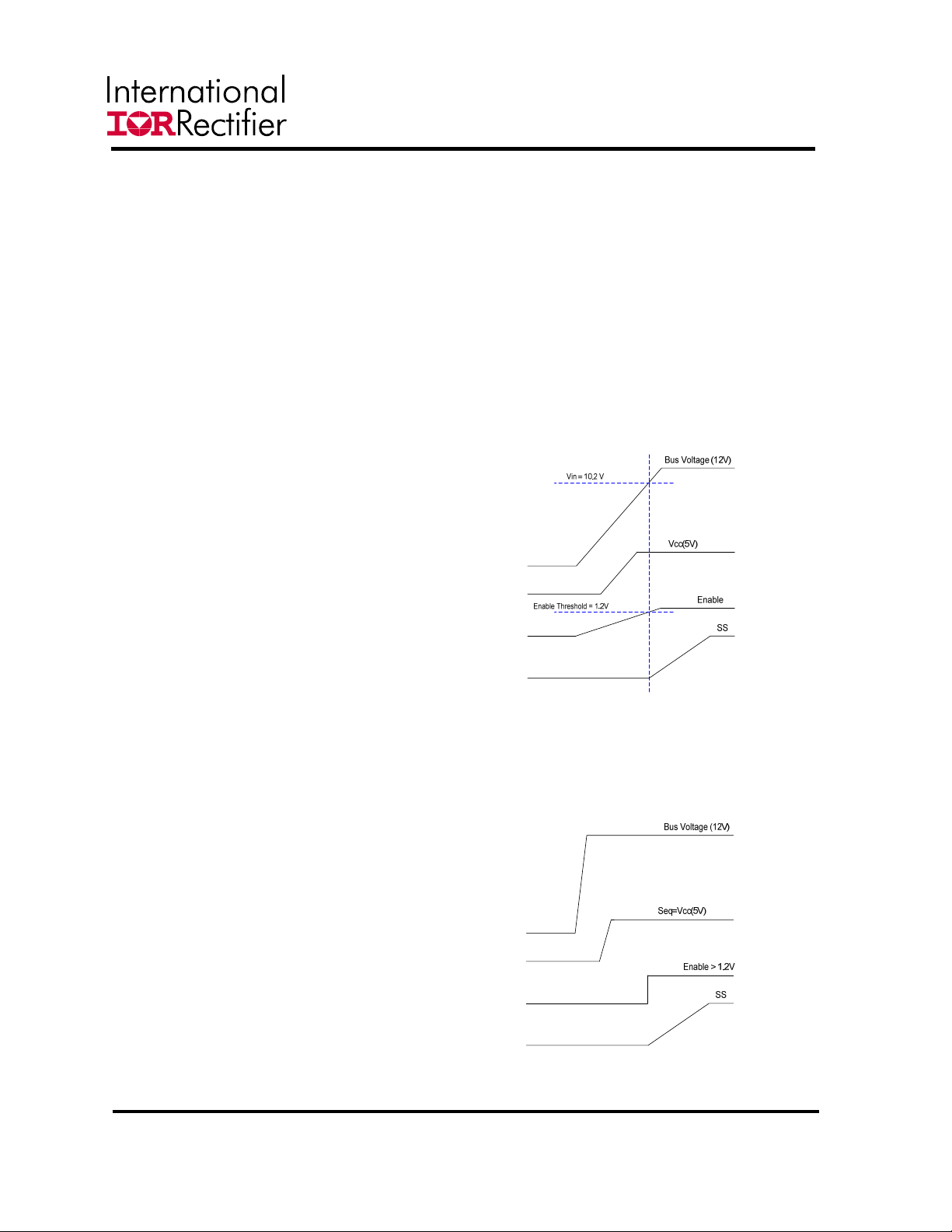
Fig. 3a: Normal Start up, Device turns on
when the Bus voltage reaches 10.2V
Figure 3b shows the recommended start-up
sequence for the non-sequenced operation of
IR3640, when Enable is used as a logic input.
Fig. 3b: Recommended startup sequence,
Non-Sequenced operation
9
(
Figure 3c shows the recommended startup
sequence for sequenced operation of IR3640
with Enable used as logic input.
Fig. 3c. Recommended startup sequence,
Sequenced operation
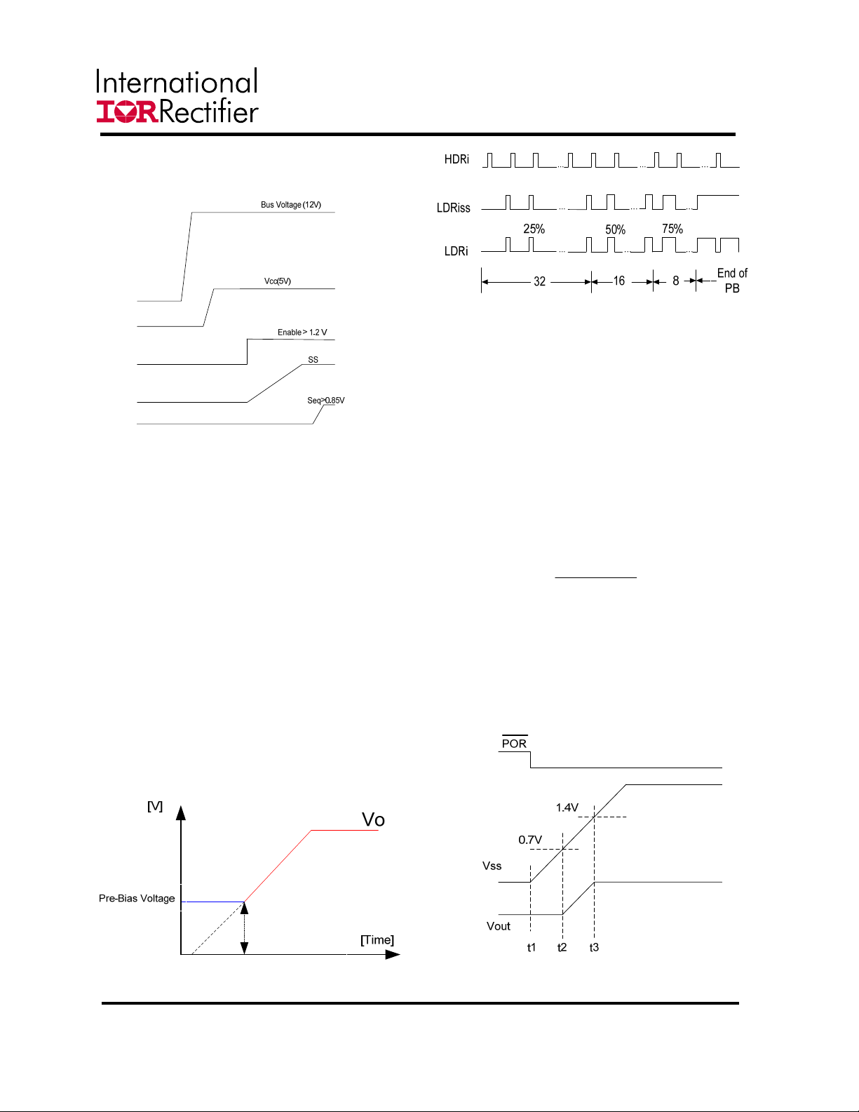
Pre-Bias Startup
IR3640 is able to start up into pre-charged
output, which prevents oscillation and
disturbances of the output voltage.
The output starts in asynchronous fashion and
keeps the synchronous MOSFET off until the first
gate signal for control MOSFET is generated.
Figure 4 shows a typical Pre-Bias condition at
start up.
The synchronous MOSFET always starts with a
narrow pulse width and gradually increases its
duty cycle with a step of 25%, 50%, 75% and
100% until it reaches the steady state value. The
number of these startup pulses for the
synchronous MOSFET is internally programmed.
Figure 5 shows a series of 32, 16, 8 startup
pulses.
IR3640MPBF
Fig. 5. Pre-Bias startup pulses
Soft-Start
The IR3640 has a programmable soft-start to
control the output voltage rise and limit the
current surge at the start-up. To ensure correct
start-up, the soft-start sequence initiates when
the Enable and Vcc rise above their UVLO
thresholds and generate the Power On Ready
(POR) signal. The internal current source
(typically 20uA) charges the external capacitor
C
linearly from 0V to 3V. Figure 6 shows the
ss
waveforms during the soft start.
The start up time can be estimated by:
)
*0.7-1.4
C
T =
start
During the soft start the OCP is enabled to
protect the device for any short circuit and over
current condition.
The SS pin can be used as shutdown signal,
pulling low this pin will result to turning off the
high side driver and turning on the low side
driver.
SS
μ
A20
(1) --
Fig. 4. Pre-Bias startup
06/15/2009
Fig. 6. Theoretical operation waveforms
during soft-start
10

Operating Frequency
−∗=
The switching frequency can be programmed
between 250kHz – 1500kHz by using an external
resistor from R
oscillator frequency versus R
to Gnd. Table 1 tabulates the
t
. Trailing edge
t
modulation is used for generating PWM
signal(Fig.7) .
Table 1. Switching Frequency and
I
vs. External Resistor (R
OCSet
I
I
ocset
ocset
29.430047.5
29.430047.5
39.240035.7
39.240035.7
48.750028.7
48.750028.7
59.0760023.7
59.0760023.7
68.270020.5
68.270020.5
78.680017.8
78.680017.8
88.690015.8
88.690015.8
97.9100014.3
97.9100014.3
110.2110012.7
110.2110012.7
121.7120011.5
121.7120011.5
130.8130010.7
130.8130010.7
143.414009.76
143.414009.76
150.315009.31
150.315009.31
)
t
(μA)Fs (kHz)Rt (kΩ)
(μA)Fs (kHz)Rt (kΩ)
IR3640MPBF
Over-Current Protection
The over current protection is performed by
sensing current through the R
MOSFET. This method enhances the converter’s
efficiency and reduce cost by eliminating a
current sense resistor. As shown in Fig. 8, an
external resistor (R
is connected between
OCset
OCSet pin and the drain of low side MOSFET
(Q2) which sets the current limit set point.
The internal current source develops a voltage
across R
current (I
. An internal current source sources
SET
) out of the OCSet pin. This
OCSet
current is a function of the switching frequency
and hence, of R
. Table 1. shows I
t
different switching frequencies.
1400
I
OCSET
)μA(Ω=
)(k
R
t
I
OCSet
IR3640
SET
R
OCSet
Hiccup
Control
DS(on)
of low side
OCSet
)2(--
Q1
Q2
L1
OUT
V
at
Ramp
V
C
Clock
Cntl gate
Sync gate
Fig. 7: Trailing-edge Modulation
Frequency Synchronization
The IR3640 is capable of accepting an external
digital synchronization signal. Synchronization
will be enabled by the rising edge at an external
clock. The switching frequency is set by
external resistor (R
). During synchronization, R
t
t
is selected such that the free running frequency
is 20% below the synchronization frequency.
When unused, the sync pin will remain floating
and is noise immune.
06/15/2009
Fig. 8: Connection of over current sensing resistor
When the low side MOSFET is turned on, the
inductor current flows through the Q2 and results
a voltage which is given by:
RRIV
∗
OCSetOCSetOCSet
L
)
(onDS
I
-(3)- ) () (
An over current is detected if the OCSet pin goes
below ground. Hence, at the current limit
threshold, V
setting I
Limit
=0. Then, for a current limit
OCset
,R
R
is calculated as follows:
OCSet
*
OCSet
=
I
OCSet
)(
IR
LimitonDS
-(4)-
11

IR3640MPBF
An over-current detection trips the OCP
comparator, latches OCP signal and cycles
the soft start function in hiccup mode.
The hiccup is performed by shorting the softstart capacitor to ground and counting the
number of switching cycles. The soft start pin
is held low until 4096 cycles have been
completed. The OCP signal resets and the
converter recovers. After every soft start cycle,
the converter stays in this mode until the
overload or short circuit is removed.
The OCP circuit starts sampling current
typically 160 ns after the low gate drive rises
to about 3V. This delay functions to filter out
switching noise.
The value of R
should be checked in an
OCSet
actual circuit to ensure that the over current
protection circuit activates as expected.
Shutdown
The IR3640 can be shutdown by pulling the
Enable pin below its 1 V threshold. This will tristate both, the high side driver as well as the
low side driver. Alternatively, the output can be
shutdown by pulling the soft-start pin below
0.3V. In shutdown by this method, the high side
driver is turned off, and the low side driver is
turned on. Thus, in this method, the output
voltage can be actively discharged through the
synchronous FET. Normal operation is
resumed by cycling the voltage at the Soft Start
pin.
Output Voltage Sequencing
The IR3640 can accommodate a full spectrum
of user programmable sequencing option
using Seq, Enable and Power Good pins.
Vo1
Vo2
Simultaneous Powerup
Fig. 9a: Simultaneous Power-up of the slave
with respect to the master.
Through these pins, voltage sequencing such as
simultaneous, sequential, etc. can be
implemented. Figure 9b shows simultaneous
sequencing configurations. In simultaneous
powerup, the voltage at the Seq pin of the slave
reaches 0.7V before the Fb pin of the master. For
R
E/RF=RC/RD
, therefore, the output voltage of
the slave follows that of the master until the
voltage at the Seq pin of the slave reaches 0.7 V.
After the voltage at the Seq pin of the slave
exceeds 0.85V, the internal 0.7V reference of
the slave dictates its output voltage.
Vin1
Vcc
Boot
Enable
Vo (Master)
RE
RF
PGood1
Vin2
Vcc
PGood2
Seq>0.85V
(steady state)
Vcc
PGood
Seq
Rt
SS/ SD
Vcc
PGood
Seq
Rt
SS/ SD
Gnd
Enable
Gnd
Sync
Sync
Comp
Boot
Comp
HDrv
OCSet
LDrv
PGnd
Vsns
OCSet
SW
Fb
HDrv
LDrv
PGnd
Vsns
RA
RB
SW
RC
Fb
RD
Vo (Master)
Vo (Salve)
06/15/2009
Note: Vo (Master) > Vo (Salve)
Fig. 9b: Application Circuit for
Simultaneous Sequencing
12

Thermal Shutdown
Temperature sensing is provided inside IR3640.
The trip threshold is typically set to 140
trip threshold is exceeded, thermal shutdown
turns off both MOSFETs and discharges the soft
start capacitor. Automatic restart is initiated when
the sensed temperature drops within the
operating range. There is a 20
the thermal shutdown threshold
Power Good and Over-voltage Protection
The IC continually monitors the output voltage via
sense pin. The Vsns voltage compares to a fixed
voltage. As soon as the sensed voltage reaches
0.88*Vref, the Power Good signal flags. Power
Good pin needs to be externally pulled high. High
state indicates that output is in regulation. Figure
10a and 10b shows the timing diagrams of Power
Good function.
If the output voltage exceeds the over voltage
threshold, an over voltage trip signal asserts, this
will result to turn off the high side driver and turn
on the low side driver until the Vsns voltage
drops below 1.15*Vref threshold. Both drivers are
latched off until a reset performed by cycling
either Vcc or Enable.
The OVP threshold can be externally
programmed to user defined value. Figure 10c
shows the response in over-voltage condition.
o
.
o
C. When
C hysteresis in
IR3640MPBF
Fig.10b: IR3640 Sequencing
Power Up
06/15/2009
Fig.10c: IR3640 Timing Diagram of Over-
voltage Protection
Fig.10a: IR3640 Non-Sequencing
Power Up (Seq=Vcc)
13

IR3640MPBF
Minimum on time Considerations
The minimum ON time is the shortest amount of
time for which the Control FET may be reliably
turned on, and this depends on the internal
timing delays. For the IR3640, the typical
minimum on-time is specified as 50 ns.
Any design or application using the IR3640 must
ensure operation with a pulse width that is higher
than this minimum on-time and preferably higher
than 100 ns. This is necessary for the circuit to
operate without jitter and pulse-skipping, which
can cause high inductor current ripple and high
output voltage ripple.
D
t
on
=
F
s
V
out
=
F
V
×
s
in
In any application that uses the IR3640, the
following condition must be satisfied:
tt
t
on
(min)
(min)
≤
onon
V
out
≤∴
FV
sin
FV
×
sin
V
out
≤×∴
t
(min)
on
The minimum output voltage is limited by the
reference voltage and hence V
Therefore, for V
out(min)
= 0.7 V,
out(min)
= 0.7 V.
Maximum Duty Ratio Considerations
A fixed off-time of 200 ns maximum is specified
for the IR3640. This provides an upper limit on
the operating duty ratio at any given switching
frequency. It is clear, that higher the switching
frequency, the lower is the maximum duty ratio at
which the IR3640 can operate. To allow some
margin, the maximum operating duty ratio in any
application using the IR3640 should still
accommodate about 250 ns off-time. Figure 11
shows a plot of the maximum duty ratio vs. the
switching frequency, with 250 ns off-time.
Max Duty Cycle
95
90
85
80
75
70
65
60
Max Duty Cycle (%)
55
250 450 650 850 1050 1250 1450 1650
Switching Frequency (kHz)
Fig. 11: Maximum duty cycle vs. switching
frequency
V
V
≤×∴
F
in
s
V
F
in
s
(min)
out
t
(min)
on
V0.7
ns 100
6
V/s
107 ×=≤×∴
Therefore, at the maximum recommended input
voltage 24V and minimum output voltage, the
converter should be designed at a switching
frequency that does not exceed 292 kHz.
Conversely, for operation at the maximum
recommended operating frequency 1.65 MHz
and minimum output voltage, any voltage above
4.2 V may not be stepped down without pulseskipping.
06/15/2009
14

IR3640MPBF
Application Information
Design Example:
The following example is a typical application for
IR3640. The application circuit is shown on page
23.
max21312
in
81
V.=V
o
25
A=I
o
mV
54
≤
ΔV
o
kHz=F
600
s
Enabling the IR3640
As explained earlier, the precise threshold of
the Enable lends itself well to implementation of
a UVLO for the Bus Voltage.
IR3640
IR3640
Enable
)V,.V,(=V
V
in
R
1
R
2
Output Voltage Programming
Output voltage is programmed by reference
voltage and external voltage divider. The Fb pin
is the inverting input of the error amplifier, which
is internally referenced to 0.7V. The divider is
ratioed to provide 0.7V at the Fb pin when the
output is at its desired value. The output voltage
is defined by using the following equation:
⎛
⎜
VV
refo
⎜
⎝
⎞
R
8
⎟
-(7)- 1
+∗=
⎟
R
9
⎠
When an external resistor divider is connected to
the output as shown in figure 11.
V
OUT
IR3640
IR3624
R
8
Fb
R
9
Fig. 13: Typical application of the IR3640 for
programming the output voltage
Fig. 12: Typical application of the IR3640 for
programming the Enable threshold
For a typical Enable threshold of V
R
2
RR
+
21
V
RR
12
EN
min
==
ENin
−
VV
EN)in(
=10.1V, R1=4.99K and R2=681 ohm
For a V
V
in (min)
(min)
=
= 1.2 V
EN
-(6)-
is a good choice.
Programming the frequency
For Fs= 600 kHz, select R
= 23.7 kΩ, using
t
Table. 1.
06/15/2009
Equation (7) can be rewritten as:
⎛
⎜
RR
∗=
⎜
⎝
V
-(5)- 1.2*
For the calculated values of R
⎞
V
ref
⎟
-(8)- 89
⎟
VV
−
refO
⎠
and R9see
8
feedback compensation section.
Soft-Start Programming
The soft-start timing can be programmed by
selecting the soft-start capacitance value. The
start-up time of the converter can be calculated
by using:
Where T
C
=
SS
is the desired start-up time (ms).
start
20uA*Tstart
()
0.71.4
-(9)-
V−
For a start-up time of 3.5ms, the soft-start
capacitor will be 0.099uF. Choose a ceramic
capacitor at 0.1uF.
15

IR3640MPBF
Δ
Bootstrap Capacitor Selection
To drive the high side switch, it is necessary to
supply a gate voltage at least 4V greater than the
bus voltage. This is achieved by using a
bootstrap configuration, which comprises the
internal bootstrap diode and an external
capacitor (C6). The operation of the circuit is as
follows: When the lower MOSFET is turned on,
the capacitor node connected to SW is pulled
down to ground. The capacitor charges towards
through the internal bootstrap diode, which
PV
cc
has a forward voltage drop V
. The voltage V
D
C
across the bootstrap capacitor C6 is
approximately given as
−≅
10) ( --VPVV
DCCC
When the upper MOSFET turns on in the next
cycle, the capacitor node connected to SW rises
to the bus voltage V
C6 is appropriately chosen, the voltage V
. However, if the value of
in
C
across C6 remains approximately unchanged
and the voltage at the Boot pin becomes
VPVVV −+≅
DccinBoot
-(11)-
Input Capacitor Selection
The ripple current generated during the on time
of upper the MOSFET should be provided by the
input capacitor. The RMS value of this ripple is
expressed by:
oRMS
D =
−∗∗=
V
o
V
in
(12))1( --DDII
-(13)-
Where:
D is the Duty Cycle
is the RMS value of the input capacitor
I
RMS
current.
Io is the output current.
For Io=25A and D=0.15, the I
RMS
=8.9A.
Ceramic capacitors are recommended due to
their peak current capabilities, they also feature
low ESR and ESL at higher frequency which
enables better efficiency. For this application, it is
advisable to have 4x10uF 25V ceramic
capacitors GRM31CR61E106KA12L from Murata
Electronics. In addition to these, although not
mandatory, a 2X330uF, 25V SMD capacitor
EEV-FK1E331P may also be used as a bulk
capacitor.
Fig. 14: Bootstrap circuit to generate
Vc voltage
A capacitor in the range of 0.1uF is generally
adequate for most applications.
06/15/2009
Inductor Selection
The inductor is selected based on output power,
operating frequency and efficiency requirements.
A low inductor value causes large ripple current,
resulting in the smaller size, faster response to a
load transient but poor efficiency and high output
noise. Generally, the selection of the inductor
value can be reduced to the desired maximum
ripple current in the inductor . The optimum
)( i
point is usually found between 20% and 50%
ripple of the output current.
For the buck converter, the inductor value for the
desired operating ripple current can be
determined using the following relation:
16

i
Δ
LVV
∗=−
oin
()
;
t
Δ
VVL
∗−=
oin
1
Dt
∗=Δ
F
V
s
o
Δ∗
FiV
*
sin
-(14)-
Where:
=
in
=
o
=
Δ
=
s
=
Δ
=
If , then the output inductor is
Voltage OutputV
time on Turnt
cycle DutyD
)%(35oIi ≈Δ
voltage input MaximumV
current ripple Inductori
frequency SwitchingF
calculated to be 0.29uH. Select L=0.33uH
The MPL104-R33 from Delta provides a
compact, low profile inductor suitable for this
application.
Output Capacitor Selection
The voltage ripple and transient requirements
determine the output capacitors type and values.
The criteria is normally based on the value of the
Effective Series Resistance (ESR). However the
actual capacitance value and the Equivalent
Series Inductance (ESL) are other contributing
components. These components can be
described as:
Δ+Δ+Δ=Δ
VVVV
)()()(
CoESLoESRoo
Δ=Δ
)(
⎛
=Δ
V
⎜
)(
ESLo
⎝
=Δ
V
Co
)(
*
ESRIV
LESRo
V
⎞
in
*
ESL
⎟
L
⎠
Δ
I
L
**8
FC
so
IR3640MPBF
Since the output capacitor has a major role in the
overall performance of the converter and
determines the result of transient response,
selection of the capacitor is critical. The IR3840
can perform well with all types of capacitors.
As a rule, the capacitor must have low enough
ESR to meet output ripple and load transient
requirements.
The goal for this design is to meet the voltage
ripple requirement in the smallest possible
capacitor size. Therefore it is advisable to select
ceramic capacitors due to their low ESR and ESL
and small size. Ten of the Murata
GRM21BR60G476ME15L (47uF/4V) capacitors
is a good choice.
Power MOSFET Selection
The IR3640 uses two N-Channel MOSFETs per
channel. The selection criteria to meet power
transfer requirements are based on maximum
drain-source voltage (V
voltage (V
resistance R
), maximum output current, On-
gs
, and thermal management.
DS(on)
The MOSFET must have a maximum operating
voltage (V
voltage (V
) exceeding the maximum input
DSS
).
in
The gate drive requirement is almost the same
for both MOSFETs. A logic-level transistor can
be used and caution should be taken with
devices at very low gate threshold voltage (V
to prevent undesired turn-on of the
complementary MOSFET, which results in a
shoot-through current.
The total power dissipation for MOSFETs
includes conduction and switching losses. For
the Buck converter the average inductor current
is equal to the DC load current. The conduction
loss is defined as:
), gate-source drive
DSS
)
gs
06/15/2009
=Δ
V
o
=Δ
L
ripple ltage Output vo
current rippleInductor I
=
ϑ
ds(on)
2
loadcond
2
loadcond
ds(on)
ds(on)
DRIswitch)(upper P
∗∗∗=
ϑ
D)(1RIswitch)(lower P
∗−∗∗=
ϑ
dependency ure temperat R
17

The R
e
=
y
=
temperature dependency should be
DS(on)
considered for the worst case operation. This is
typically given in the MOSFET datasheet. Ensure
that the conduction losses and switching losses
do not exceed the package ratings or violate the
overall thermal budget.
For this design, the IRF6710 is selected for
control FET and IRF6795 is selected for the
synchronous FET. These devices provide low on
resistance in a DirectFET package.
The MOSFETs have the following data:
:(IRF6710) ControlFET
nCV,QV
8.825
==
gds
VVmΩR
5.4@0.9
==
gsds(on)
The conduction losses will be: P
gds
cond
:(IRF6795) SyncFET
nC V,QV
3525
==
==
gsds(on)
=2.12W at
VVmΩR
5.4@4.2
Io=25A. The switching loss is more difficult to
calculate, even though the switching transition is
well understood. The reason is the effect of the
parasitic components and switching times, such
as turn-on / turn-off delays and rise and fall
times. The control MOSFET contributes to the
majority of the switching losses in a synchronous
Buck converter. The synchronous MOSFET turns
on under zero voltage conditions, therefore, the
turn on losses for synchronous MOSFET can be
neglected. With a linear approximation, the total
switching loss can be expressed as:
ttV
)(
Where:
V
t
t
= Drain to source voltage at the off time
ds(off)
= Rise time
r
= Fall time
f
P+=
sw
froffds
2
I
T
load
-(15)- **
T = Switching period
I
= Load current
load
The switching time waveforms is shown in Fig.
15.
From IRF6710 data sheet:
tr = 20ns
tf = 6ns
These values are taken under a certain test
condition. For more details please refer to the
IRF6710 data sheet.
IR3640MPBF
V
DS
90%
10%
V
GS
t
d
t
d
(ON)
Fig. 15: Switching time waveforms
By using equation (15), we can calculate the
switching losses. P
sw
The reverse recovery loss is also another
contributing factor in control FET switching
losses. This is equivalent to extra current
required to remove the minority charges from the
synchronous FET. The reverse recovery loss can
be expressed as:
:Q
rr
: V
in
: F
s
The gate driving loss is the power consumption
to drive both the control and synchronous FETs.
The gate driving loss can be estimated as:
:Q
g
: V
g
: F
s
Feedback Compensation
The IR3640 is a voltage mode controller. The
control loop is a single voltage feedback path
including error amplifier and error comparator. To
achieve fast transient response and accurate
output regulation, a compensation circuit is
necessary. The goal of the compensation
network is to provide a closed-loop transfer
function with the highest 0dB crossing frequency
and adequate phase margin (greater than 45
(OFF)
t
r
=2.34W at Io=25A.
*F*VQP
sinrrQrr
Recovery Reverse
Charg
Voltage BusInput
Frequency Switching
*F*VQP
sggDriver
Charge Gate Total
Voltage Driving Gate
Frequenc
Switching
t
f
o
).
06/15/2009
18

The output LC filter introduces a double pole,
)
)
(
)
≤
)
–40dB/decade gain slope above its corner
resonant frequency, and a total phase lag of 180
o
(see Fig. 16). The resonant frequency of the LC
filter is expressed as follows:
1
=
LC
π
2
-(16)-
CLF∗∗
oo
Figure 16 shows gain and phase of the LC filter.
o
Since we already have 180
phase shift from the
output filter alone , the system risks being
unstable.
H(s) dB
Z
IN
Gain(dB)
IR3640MPBF
OUT
V
8
R
Fb
9
R
REF
V
R
3
E/A
C
POLE
C4
f
Z
Ve
Comp
0dB
Gain
-40dB/decade
LC
F
Frequency
-180
Phase
0
o
LC
F
Frequency
Fig. 16: Gain and Phase of LC filter
The IR3640 uses a voltage-type error amplifier
with high-gain (110dB) and wide-bandwidth. The
output of it is available for DC gain control or AC
phase compensation.
The error amplifier can be compensated either in
type II or type III compensation. When it is used
in type II compensation, a series RC circuit from
Comp pin to ground as shown in figure 16 is
used.
This method requires the output capacitor should
have enough ESR to satisfy stability
requirements. In general the output capacitor’s
ESR generates a zero typically at 5kHz to 50kHz
which is essential for an acceptable phase
margin.
The ESR zero of the output capacitor expressed
as follows:
F
=
ESR
1
π
∗
**2
-(17
-
CESR
o
F
Z
F
POLE
Frequency
Fig. 17: TypeII compensation network
and its asymptotic gain plot
The transfer function (Ve/Vo) is given by:
V
e
V
o
Z
)(
sH
Z
+
1
f
IN
CsR
−=−==
43
CsR
48
-(18)-
The (s) indicates that the transfer function varies
as a function of frequency. This configuration
introduces a gain and zero, expressed by:
R
3
()
sH
=
R
8
F
1
=
z
2
-(19)-
-(20
-
*Cπ*R
43
First select the desired zero-crossover frequency
(Fo):
>
F1/10~1/5F and FF *
soESRo
Use the following equation to calculate R3:
R =
3
ESRoosc
2
*
FV
LCin
-(21
-
***
RFFV
8
Where:
= Maximum Input Voltage
V
in
= Oscillator Ramp Voltage
V
osc
= Crossover Frequency
F
o
= Zero Frequency of the Output Capacitor
F
ESR
= Resonant Frequency of the Output Filter
F
LC
= Feedback Resistor
R
8
06/15/2009
19

IR3640MPBF
+
=
To cancel one of the LC filter poles, place the
zero before the LC filter resonant frequency pole:
FF
%75
=
LCz
F
=
z
1
*75.0
π
*2
-(22)-
CL
oo
Using equations (15) and (16) to calculate C4.
One more capacitor is sometimes added in
parallel with C4 and R3. This introduces one
more pole which is mainly used to suppress the
switching noise.
The additional pole is given by:
F
=
P
1
**
R2
π
3
*
CC
POLE4
+
CC
POLE4
The pole sets to one half of the switching
frequency which results in the capacitor C
C
POLE
=
1
1
−
π
FR
**
3
s
C
4
1
≅
π
F
*R*
s
3
POLE
:
For a general solution for unconditional stability
for any type of output capacitors, in a wide range
of ESR values we should implement local
feedback with a compensation network (type III).
The typically used compensation network for
voltage-mode controller is shown in Fig. 17.
In such configuration, the transfer function is
given by:
Z
V
e
V
o
f
−=
Z
IN
OUT
C
10
R
Gain(dB)
V
3
C
7
8
R
Fb
9
R
REF
V
3
R
E/A
4
C
Comp
f
Z
Ve
IN
Z
H(s) dB
1
Z
F
2
Z
F
2
P
F
F
3
P
Frequency
Fig.18: Compensation network with local
feedback and its asymptotic gain plot
The compensation network has three poles and
two zeros and they are expressed as follows:
0F
1P
F
=
2P
=
F
3P
F
=
1z
F
=
2z
1
π
*
π
710
1
⎛
⎜
R2
3
⎜
⎝
⎞
*
CC
34
⎟
⎟
+
CC
34
⎠
1
≅
**
π
CR2
33
CR2
**
1
**
π
CR2
43
1
RRC2
+
1
≅
**)(**
ππ
RC2
871087
Cross over frequency is expressed as:
By replacing Z
and Zfaccording to Fig. 17, the
in
transfer function can be expressed as:
V
=
in
CRF
73o
V
1
***
CL2
π
**
ooosc
Based on the frequency of the zero generated by
()
[]
1
−
)(
sH
=
*
)(
CCsR
+
⎡
348
1
sR
+
⎢
⎣
1*)1(
++
⎤
⎛
⎜
3
⎜
⎝
⎞
*
CC
34
⎟
⎥
⎟
CC
+
34
⎠
⎦
RRsCCsR
108743
)1(*
CsR
+
710
the output capacitor and its ESR versus
crossover frequency, the compensation type can
be different. Table 2 below shows the
compensation types and location of the
crossover frequency.
06/15/2009
20

IR3640MPBF
p
Table 2 The compensation type and location
of F
Compensator
Compensator
Type
Type
Type III
Type III
versus F
ESR
F
F
vs F
vs F
ESR
ESR
F
F
LC<FES R<Fo<Fs
LC<FES R<Fo<Fs
F
F
LC<Fo<FESR
LC<Fo<FESR
o
o
o
Output
Output
Capacitor
Capacitor
Electrolytic
Electrolytic
/2Type II
/2Type II
Tantalum
Tantalum
Tantalum
Tantalum
Ceramic
Ceramic
The higher the crossover frequency, the
potentially faster the load transient response.
However, the crossover frequency should be low
enough to allow attenuation of switching noise.
Typically, the control loop bandwidth or
crossover frequency is selected such that
()
F F * 1/10~1/5≤
so
The DC gain should be large enough to provide
high DC-regulation accuracy. The phase margin
should be greater than 45
o
for overall stability.
These result to:
FLC=18.3kHz
F
=2306kHz
ESR
F
=300kHz
s/2
Select crossover frequency:
Fo=100kHz
Since: FLC<Fo<F
S/2<FESR
, TypeIII is selected to
place the pole and zeros. Detailed calculation of
compensation TypeIII:
o
=Θ
70 Margin Phase Desired
sin1
FF
=
2
oZ
FF
=
2
oP
3
Θ−
=
sin1
Θ+
sin1
Θ+
=
sin1
Θ−
FF
ZZ
FF
==
sP
kHz
17.63
kHz 567.1
==
21
and kHz 8.82 *5.0 :Select
kHz 300*0.5
For this design we have:
=12V
V
in
V
=1.8V
o
V
=1.8V
osc
V
=0.7V
ref
L
=0.33uH
o
C
=10x47uF(ceramic)
o
It must be noted here that the value of the
capacitance used in the compensator design
must be the small signal value. For instance, the
small signal capacitance of the 47uF capacitor
used in this design is 23uF at 1.8 V DC bias and
600 kHz frequency. It is this value that must be
used for all computations related to the
compensation. The small signal value may be
obtained from the manufacturer’s datasheets,
design tools or SPICE models. Alternatively,
they may also be inferred from measuring the
power stage transfer function of the converter
and measuring the double pole frequency F
LC
and using equation (16) to compute the small
signal C
.
o
nF 2.2C :Select
=
7
: and , Calculate
CCR
433
****2
π
R
3
7
VCLF
oscooo
R
*
VC
in
3
k 3.25;
Ω==
k 3.24 :Select
R
3
C
4
C
3
R
10
1
π
1
π
π
Ω=
**2
RF
1
Z
3
**2
RF
33
P
: and , Calculate
RRR
9810
1
**2
FC
P
27
CC
nF 6.5 :Select nF, 57.5 ;
===
44
F 160 :Select ,pF 74.163 ;
===
CC
33
RR
1010
Ω=Ω== 130 :Select , 130 ;
06/15/2009
21

IR3640MPBF
∗
R
8
1
**2
FC
π
Z
RR
27
810
,k 3.98 ;-
Ω==
k 4.02:Select
R
8
V
ref
R
-
VV
refo
Ω=
k 2.55 :Select k 2.56 ;*
RRR
9989
Ω=Ω==
Programming the Current-Limit
The Current-Limit threshold can be set by
connecting a resistor (R
) from the drain of
OCSET
the low-side MOSFET to the OCSet pin. The
resistor can be calculated by using equation (3).
The R
DS(on)
has a positive temperature
coefficient and it should be considered for the
worst case operation. This resistor must be
placed close to the IC. This IC doesn't require a
small ceramic capacitor from OCset pin to
ground.
IR
II
==
criticalLSET
)(
)(
onDS
)(
LIMoSET
OCSetOCSet
R
)(
onDS
mmR
6.35.1*4.2
==≅
Ω=Ω=
(23) --
AAII
5.375.1*25
current)output nominalover (50%
OCSet
uA
==
600kHz)Fs(at 1.59I
Ω=Ω=
KRK
26.2Select 29.2R
7OCSet
Setting the Power Good Threshold
Power Good threshold can be programmed by
using two external resistors (R6, R7 in Page 23).
The following formula can be used to set the
threshold:
R
Where: 0.88*V
out
(
ref
−=
880
*V.
ref
is reference of the internal
(24) -- *)1
R
76
*9.0
V
comparator, for IR3640, it is 0.62V
0.9*Vout is selectable threshold for power good,
for this design it is 1.62V.
Select R
Using (24): R
Select R
=2.55KOhm
7
=4.16KOhm
6
=4.12KOhm
6
Use a pull up resistor (4.99K) from PGood pin to
Vcc.
Layout Consideration
The layout is very important when designing high
frequency switching converters. Poor layout will
affect noise pickup and can cause a good design
to perform with less than expected results.
Start to place the power components, making all
the connection in the top layer with wide, copper
filled areas. The inductor, output capacitors and
the MOSFETS should be as close to each other
as possible. This helps to reduce the EMI
radiated by the power traces due to the high
switching currents through them. Place input
capacitor very close to the drain of the high-side
MOSFET.
The feedback part of the system should be kept
away from the inductor and other noise sources.
The critical bypass components such as
capacitors for Vcc and PVcc should be close to
the respective pins. It is important to place the
feedback components including feedback
resistors and compensation components close to
Fb and Comp pins.
Place the Rocset resistor close to Ocset pin and
connect this with a short trace to SW pin.
In a multilayer PCB use one layer as a power
ground plane and have a control circuit ground
(analog ground), to which all signals are
referenced. The goal is to localize the high
current path to a separate loop that does not
interfere with the more sensitive analog control
function. These two grounds must be connected
together on the PC board layout at a single point.
The MLPQ is a thermally enhanced package.
Based on thermal performance it is
recommended to use 4-layers PCB. To
effectively remove heat from the device the
exposed pad should be connected to ground
plane using vias.
06/15/2009
22

Application Diagram:
IR3640MPBF
Fig. 19: Typical Application Circuit for Non-Sequencing
12V to 1.8V, 25A Point of Load Converter
Suggested Bill of Materials for the application circuit:
Refe re nc e Va lu e Descri ption Man ufa cturer Pa rt Num be r
Cin 330uF SMD Elecrolytic, 25V,F-size,20% Panasonic EEE-FK1E331P
Cin 10uF Cerami c, 25V,1210,X5R,10% Taiy o-Yuden TMK325B J106MN-T
Co 47uF Cerami c, 4V,0805,X5R,10% Murata E lec tronic s GRM 21BR60G476ME15L
C1 1.0uF Ceramic ,25V,0603,X5R,10% Murata El ect ronics GRM188R61E 105KA12D
C2 C6 C8 0.1uF Ceramic ,50V,0603,X7R,10% Panasonic E CJ-1VB1H104K
C3 160pF Ceramic ,50V ,0603, C0G,5% Murata Elec troni cs GRM1885C1H161JA01D
C4 5.6nF Ceramic ,25V,0603,C0G,5% Panas onic-ECG C1608C0G1E562J
C7 2200pF Cerami c, 50V,0603,C0G, 5% TDK Corporation C1608C0G1H222J
L1 0.33uH SMT-Inductor,1. 5mOhm s, 10x11mm,20% Delta MPL104-R33IR
Q1 IRF6710S2TRPbF IRF6710 SQ 25V Internat ional Rec tifier IRF6710S2TRPbF
Q2 IRF6795MPbF IRF6795 MX 25V International Rect ifier IRF6795MPbF
R1 R11 4.99K Thick-film, 0603,1/ 10W, 1% Rohm MCR03EZPFX4991
R2 681 Thick -film, 0603,1/ 10 W,1% Vishey/ Dale CRCW0603681RFKE A
R3 3.24K Thick-film,0603, 1/10W, 1% Rohm MCR03EZPFX3241
R4 23.7K Thick-film,0603, 1/10W, 1% Rohm MCR03EZPFX2372
R5 2.26K Thick-film,0603, 1/10W, 1% Rohm MCR03EZPFX2261
R6 4.12K Thick-film,0603, 1/10 W, 1% Rohm MCR03E ZPFX4121
R7 R9 2.55K Thick-fil m,0603,1/10 W, 1% Rohm MCR03EZPFX2551
R8 4.02K Thick-film,0603, 1/10 W, 1% Rohm MCR03E ZPFX4021
R10 130 Thick -film, 0603,1/ 10 W,1% Rohm M CR03EZPFX1300
06/15/2009
23

Application Diagram:
IR3640MPBF
IR3640
06/15/2009
Fig. 20: Typical Circuit for Sequencing Application
24

IR3640MPBF
TYPICAL OPERATING WAVEFORMS
(Vin=12.0V, Vcc=5V, Vo=1.8V, Io=0- 25A, Room Temperature, No Air Flow, Fig.19)
Fig. 21: Start up at 0A Load
, Ch2:PGood Ch3:VSSCh4: V
Ch
1:Vo
Fig. 23: Start up with 1.5V Prebias,
0A Load, Ch
2:Vout Ch3:VSSCh4
: PGood
Fig. 22: Start up at 25A Load
Ch
in
, Ch2:PGood Ch3:VSSCh4: V
1:Vo
in
Fig. 24: Output Voltage Ripple, 25A load
Ch
: V
3
out
Fig. 25: Inductor node at 25A load
Ch
:SW
2
06/15/2009
Fig. 26: Short (Hiccup) Recovery
Ch
2:Vout
, Ch3:V
, Ch4:Io
SS
25

TYPICAL OPERATING WAVEFORMS
(Vin=12V, Vcc=5V, Vo=1.8V, Room Temperature, No Air Flow, Fig.19)
IR3640MPBF
06/15/2009
Fig. 27: Transient Response
0A-12.5A load Ch
2:Vout
, Ch4:I
o
26

IR3640MPBF
TYPICAL OPERATING WAVEFORMS
(Vin=12V, Vcc=5V, Vo=1.8V, Io=0-25A, Room Temperature, No Air Flow, Fig.19)
Fig.28: Bode Plot at 25A load shows a bandwidth of 113.6kHz and phase margin of 50.4 degrees
06/15/2009
27

TYPICAL OPERATING WAVEFORMS
(Vin=12V, Vo=1.8V, Io=0-25A, Room Temperature, No Air Flow, Fig.19)
IR3640_IRF6710_IRF6795_0.33uH Efficiency vs. Io
95
90
85
80
Efficiency(%)
75
70
135791113151719212325
Io(A)
IR3640MPBF
IR3640_IRF6710_IRF6795_0.33uH Power Loss vs. Io
7
6
5
4
3
Ploss(W)
2
1
0
1 3 5 7 9 11 13 15 17 19 21 23 25
Io(A)
Fig.29: Efficiency and power loss vs. load current
06/15/2009
28

IR3640MPBF
PCB Metal and Components Placement
• Lead land width should be equal to nominal part lead width. The minimum lead to lead spacing
should be
• Lead land length should be equal to maximum part lead length + 0.3 mm outboard extension
+0.05mm inboard extension. The outboard extension ensures a large and inspectable toe fillet,
and the inboard extension will accommodate any part misalignment and ensure a fillet.
• Center pad land length and width should be equal to maximum part pad length and width.
However, the minimum metal to metal spacing should be
for 1 oz. Copper and
• Four 0.30mm diameter via shall be placed in the center of the pad land and connected to ground
to minimize the noise effect on the IC.
≥ 0.2mm to minimize shorting.
≥ 0.17mm for 2 oz. Copper (≥ 0.1mm
≥ 0.23mm for 3 oz. Copper).
06/15/2009
29

IR3640MPBF
Solder Resist
• The solder resist should be pulled away from the metal lead lands by a minimum of 0.06mm. The
solder resist mis-alignment is a maximum of 0.05mm and it is recommended that the lead lands are
all Non Solder Mask Defined (NSMD). Therefore pulling the S/R 0.06mm will always ensure NSMD
pads.
• The minimum solder resist width is 0.13mm. At the inside corner of the solder resist where the lead
land groups meet, it is recommended to provide a fillet so a solder resist width of
remains.
• The land pad should be Non Solder Mask Defined (NSMD), with a minimum pullback of the solder
resist off the copper of 0.06mm to accommodate solder resist mis-alignment.
• Ensure that the solder resist in-between the lead lands and the pad land is ≥ 0.15mm due to the
high aspect ratio of the solder resist strip separating the lead lands from the pad land.
• Each via in the land pad should be tented or plugged from bottom boardside with solder resist.
≥ 0.17mm
06/15/2009
30

IR3640MPBF
Stencil Design
• The stencil apertures for the lead lands should be approximately 80% of the area of the lead
lands. Reducing the amount of solder deposited will minimize the occurrence of lead shorts.
Since for 0.5mmpitch devices the leads are only 0.25mm wide, the stencil apertures should not
be made narrower; openings in stencils < 0.25mm wide are difficult to maintain repeatable solder
release.
• The stencil lead land apertures should therefore be shortened in length by 80% and centered on
the lead land.
• The land pad aperture should deposit approximately 50% area of solder on the center pad. If too
much solder is deposited on the center pad the part will float and the lead lands will be open.
• The maximum length and width of the land pad stencil aperture should be equal to the solder
resist opening minus an annular 0.2mm pull back to decrease the incidence of shorting the center
land to the lead lands when the part is pushed into the solder paste.
06/15/2009
31

IR3640MPBF
06/15/2009
IR WORLD HEADQUARTERS: 233 Kansas St., El Segundo, California 90245, USA Tel: (310) 252-7105
TAC Fax: (310) 252-7903
This product has been designed and qualified for the Industrial market.
Visit us at www.irf.com for sales contact information
Data and specifications subject to change without notice. 11/07
32
 Loading...