

Page 1
Data Sheet No. PD-6.029G
Next Data SheetIndex
Previous Datasheet
To Order
IR2155
SELF-OSCILLATING HALF-BRIDGE DRIVER
Features
n Floating channel designed for bootstrap operation
Fully operational to +600V
Tolerant to negative transient voltage
dV/dt immune
n Undervoltage lockout
n Programmable oscillator frequency
f =
1.4 (R 150 ) C
nMatched propagation delay for both channels
n Micropower supply startup current of 125 µA typ.
n Low side output in phase with R
1
×+ ×
Ω
TT
T
Description
The IR2155 is a high voltage, high speed, self-oscillating power MOSFET and IGBT driver with both high
and low side referenced output channels. Proprietary
HVIC and latch immune CMOS technologies enable
ruggedized monolithic construction. The front end features a programmable oscillator which is similar to the
555 timer. The output drivers feature a high pulse current buff er stage and an internal deadtime designed f or
minimum driver cross-conduction. Propagation dela ys
for the two channels are matched to simplify use in
50% duty cycle applications. The floating channel can
be used to drive an N-channel power MOSFET or IGBT
Product Summary
V
OFFSET
Duty Cycle 50%
IO+/- 210 mA / 420 mA
V
OUT
Deadtime (typ.) 1.2 µs
600V max.
10 - 20V
Package
in the high side configuration that operates off a high
voltage rail up to 600 volts.
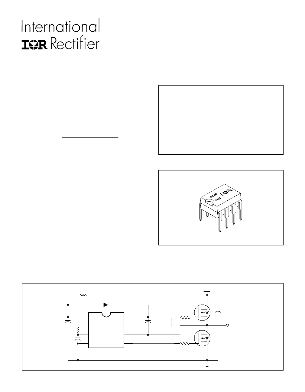
Typical Connection
up to 600V
V
CC
R
T
C
T
V
HO
V
LOCOM
B
S
TO
LOAD
ONTROL INTEGRATED CIRCUIT DESIGNERS MANUAL B-199
C
Page 2
IR2155
Next Data SheetIndex
Previous Datasheet
To Order
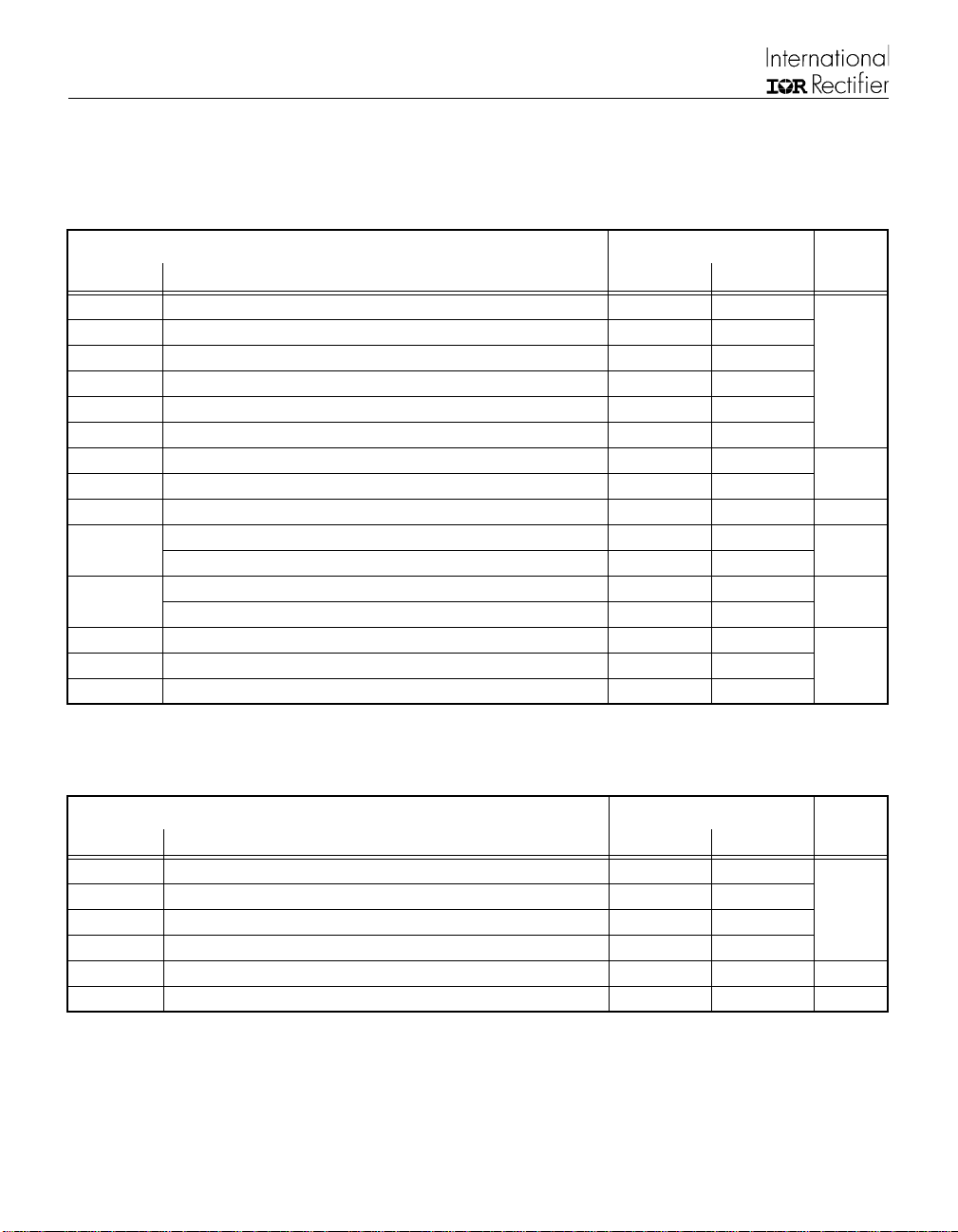
Absolute Maximum Ratings
Absolute Maximum Ratings indicate sustained limits beyond which damage to the device may occur. All voltage parameters are absolute voltages referenced to COM. The Thermal Resistance and Power Dissipation ratings are measured
under board mounted and still air conditions.
Parameter Value
Symbol Definition Min. Max. Units
V
B
V
S
V
HO
V
LO
V
RT
V
CT
I
CC
I
RT
dVs/dt Allowable Offset Supply Voltage Transient — 50 V/ns
P
D
R
θJA
T
J
T
S
T
L
High Side Floating Supply Voltage -0.3 625
High Side Floating Supply Offset Voltage VB - 25 VB + 0.3
High Side Floating Output Voltage VS - 0.3 V
Low Side Output Voltage -0.3 VCC + 0.3
RT V oltage -0.3 VCC + 0.3
CT Voltage -0.3 V
Supply Current (Note 1) — 25
RT Output Current -5 5
Package Power Dissipation @ TA ≤ +25°C (8 Lead DIP) — 1.0
(8 Lead SOIC) — 0.625
Thermal Resistance, Junction to Ambient (8 Lead DIP) — 125
(8 Lead SOIC) — 200
Junction Temperature — 150
Storage Temperature -55 150 °C
Lead Temperature (Soldering, 10 seconds) — 300
CC
B
+ 0.3
+ 0.3
mA
°C/W
V
W
Recommended Operating Conditions
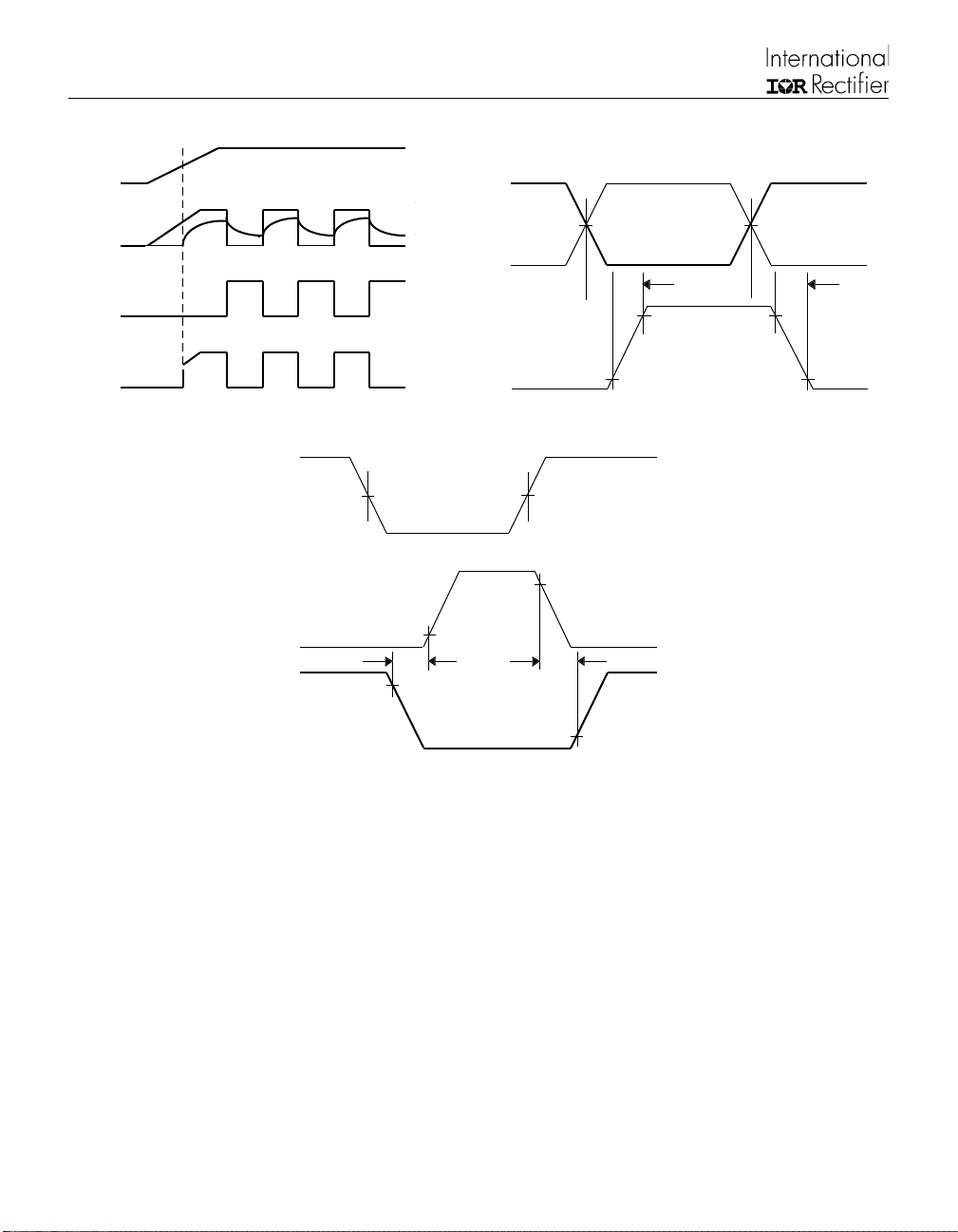
The Input/Output logic timing diagram is shown in Figure 1. For proper operation the device should be used within the
recommended conditions. The V
Symbol Definition Min. Max. Units
V
B
V
S
V
HO
V
LO
I
CC
T
A
Note 1: Because of the IR2155’s application specificity toward off-line supply systems, this IC contains a zener clamp
B-200 CONTROL INTEGRATED CIRCUIT DESIGNERS MANUAL
High Side Floating Supply Absolute Voltage VS + 10 VS + 20
High Side Floating Supply Offset Voltage — 600
High Side Floating Output Voltage V
Low Side Output Voltage 0 V
Supply Current (Note 1) — 5 mA
Ambient Temperature -40 125 °C
structure between the chip VCC and COM which has a nominal breakdown voltage of 15.6V. Therefore, the IC
supply voltage is normally derived by forcing current into the supply lead (typically by means of a high value
resistor connected between the chip V
to COM) and allowing the internal zener clamp circuit to deter mine the nominal supply voltage. There-
V
CC
fore, this circuit should not be driven by a DC, low impedance power source of greater than V
offset rating is tested with all supplies biased at 15V differential.
S
Parameter Value
S
and the rectified line voltage and a local decoupling capacitor from
CC
V
B
CC
CLAMP
V
.
Page 3
Dynamic Electrical Characteristics
To Order
Next Data SheetIndex
Previous Datasheet
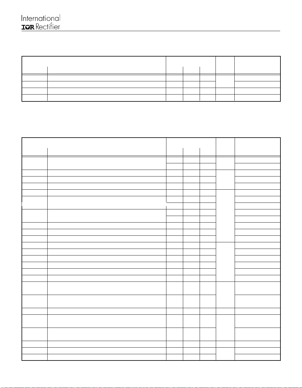
V
(VCC, VBS) = 12V, CL = 1000 pF and TA = 25°C unless otherwise specified.
BIAS
Parameter Value
Symbol Definition Min. Typ. Max. Units Test Conditions
t
t
DT Deadtime 0.50 1.20 2.25 µs
DR
Tur n-On Rise Time — 80 120
r
Tur n-Off Fall Time — 40 70
r
Duty Cycle 48 50 52 %
T
ns
Static Electrical Characteristics
V
(VCC, VBS) = 12V, CL = 1000 pF, CT = 1 nF and TA = 25°C unless otherwise specified. The VIN, VTH and I
BIAS
parameters are referenced to COM. The VO and IO parameters are referenced to COM and are applicable to the
respective output leads: HO or LO.
Parameter Value
Symbol Definition Min. Typ. Max. Units Test Conditions
f
OSC
V
CLAMP
V
CT+
V
CT-
V
CTUV
V
RT+
V
RT-
V
RTUV
V
OH
V
OL
I
LK
I
QBS
I
QBSUV
I
QCC
I
QCCUV
I
CT
V
BSUV+
V
BSUV-
V
BSUVH
V
CCUV+
V
CCUV-
V
CCUVH
I
O+
I
O-
Oscillator Frequency 19.4 20.0 20.6 RT = 35.7 kΩ
94 100 106 RT = 7.04 kΩ
kHz
VCC Zener Shunt Clamp Voltage 14.4 15.6 16.8 ICC = 5 mA
2/3 VCC Threshold 7.8 8.0 8.2 V
1/3 VCC Threshold 3.8 4.0 4.2
CT Undervoltage Lockout — 20 50 2.5V < V
RT High Level Output Voltage, VCC - R
T
— 0 100 IRT = -100 µ A
— 200 300 IRT = -1 mA
RT Low Level Output Voltage — 20 50 IRT = 100 µA
— 200 300 IRT = 1 mA
RT Undervoltage Lockout, VCC - R
High Level Output Voltage, V
Low Level Output V oltage, V
BIAS
O
- V
T
O
— 0 100 2.5V < V
— — 100 IO = 0A
— — 100 IO = 0A
mV
Offset Supply Leakage Current — — 50 VB = VS = 600V
Quiescent VBS Supply Current — 70 150
Micropower VBS Supply Startup Current — 55 125
Quiescent VCC Supply Current — 50 0 1000
µA
Micropower VCC Supply Startup Current — 70 150
CT Input Current — 0.001 1.0
VBS Supply Undervoltage Positive Going 7.7 8.4 9.2
Threshold
VBS Supply Undervoltage Negative Going 7.3 8.1 8.9
Threshold
VBS Supply Undervoltage Lockout Hysteresis 100 4 00 — mV
VCC Supply Undervoltage Positive Going 7.7 8.4 9.2
Threshold
VCC Supply Undervoltage Negative Going 7.4 8.1 8.9
Threshold
VCC Supply Undervoltage Lockout Hysteresis 200 400 — mV
Output High Short Circuit Pulsed Current 210 250 — VO = 0V
Output Low Short Circuit Pulsed Current 42 0 500 — VO = 15V
mA
IR2155
IN
< V
CC
CCUV
< V
CC
CCUV
V
V
CONTROL INTEGRATED CIRCUIT DESIGNERS MANUAL B-201
Page 4
IR2155
To Order
Next Data SheetIndex
Previous Datasheet
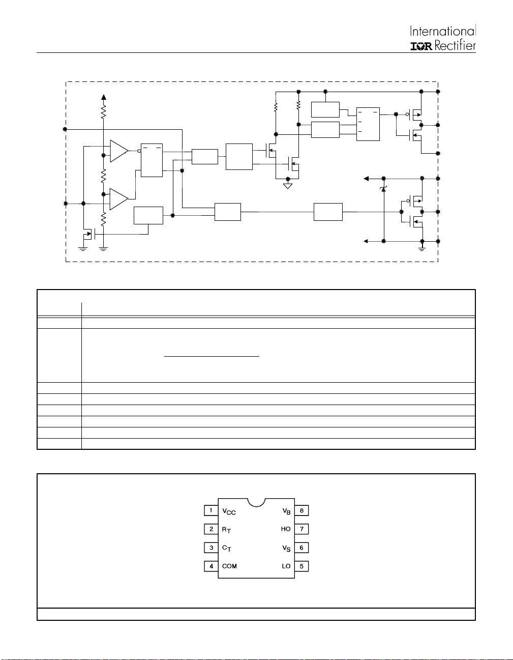
Functional Block Diagram
R
R
T
RQ
+
R
C
T
-
+
R
Lead Definitions
Lead
Symbol Description
R
T
C
T
V
B
HO High side gate dri ve output
V
S
V
CC
LO Low side gate drive output
COM Low side return
Oscillator timing resistor input,in phase with LO for normal IC operation
Oscillator timing capacitor input, the oscillator frequency according to the following equation:
where 150Ω is the effective impedance of the RT output stage
High side floating supply
High side floating supply return
Low side and logic fixed supply
SQ
UV
DETECT
f =
×+ ×
1.4 (R 150 ) C
HV
LEVEL
SHIFT
TIME
PULSE
DEAD
TIME
GEN
DEAD
1
Ω
TT
UV
DETECT
PULSE
FILTER
DELAY
R
R
S
15.6V
V
B
Q
HO
V
S
V
CC
LO
COM
Lead Assignments
B-202 CONTROL INTEGRATED CIRCUIT DESIGNERS MANUAL
8 Lead DIP
IR2155
Page 5
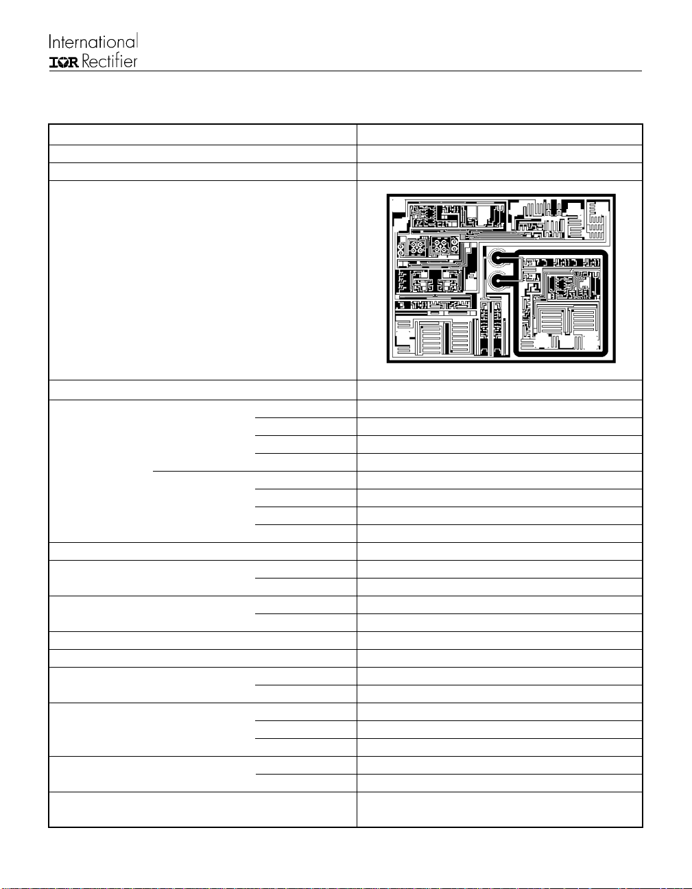
Device Information
To Order
Next Data SheetIndex
Previous Datasheet
Process & Design Rule HVDCMOS 4.0 µm
Transistor Count 260
Die Size 88 X 92 X 26 (mil)
Die Outline
Thickness of Gate Oxide 800Å
Connections Material Poly Silicon
First Width 4 µm
Layer Spacing 6 µm
Thickness 5000Å
Material Al - Si (Si: 1.0% ±0.1%)
Second Width 6 µm
Layer Spacing 9 µm
Thickness 20,000Å
Contact Hole Dimension 8 µm X 8 µm
Insulation Layer Material PSG (SiO2)
Thickness 1.5 µm
Passivation Material PSG (SiO2)
Thickness 1.5 µm
Method of Saw Full Cut
Method of Die Bond Ablebond 84 - 1
Wire Bond Method Thermo Sonic
Material Au (1.0 mil / 1.3 mil)
Leadframe Material Cu
Die Area Ag
Lead Plating Pb : Sn (37 : 63)
Pa ckage Types 8 Lead PDIP / SO-8
Materials EME6300 / MP150 / MP190
Remarks:
IR2155
CONTROL INTEGRATED CIRCUIT DESIGNERS MANUAL B-203
Page 6
IR2155
To Order
Next Data SheetIndex
Previous Datasheet
V
CLAMP
R
(HO)
T
50%
R
(LO)
T
t
r
50%
t
f
90% 90%
V
HO
V
+
CCUV
CC
R
T
C
T
LO
DT
HO
90%
10% 10%
LO
Figure 1. Input/Output Timing Diagram Figure 2. Switching Time Waveform Definitions
R
T
50% 50%
HO
LO
10%
90%
Figure 3. Deadtime Wavefor m Definitions
B-204 CONTROL INTEGRATED CIRCUIT DESIGNERS MANUAL
10%
 Loading...