

查询IR2125Z供应商
PD - 60024C
IR2125Z
CURRENT LIMITING SINGLE CHANNEL DRIVER
Features
Product Summary
n Floating channel designed for bootstrap
operation
Fully operational to +400V
Tolerant to negative transient voltage
dV/dt immune
n Gate drive supply range from 12 to 18V
n Undervoltage lockout
V
OFFSET
IO+/- 1A / 2A
V
OUT
VCSth 230 mv
t
(typ.) 150 & 150 ns
on/off
400V max.
12 - 18V
n Current detection and limiting loop to limit driven
power transistor current
n Error lead indicates fault conditions and pro
grams shutdown time
n Output in phase with input
Description
The IR2125Z is a high voltage, high speed power
MOSFET and IGBT driver with over-current limiting
protection circuitry . Proprietary GVIC and latch immune
CMOS technologies enable ruggedized minilithic
consturction. Logic inputs are compatible with standard
CMOS or LSTTL outputs. the ouput driver features a high
pulse current buffer stage designed for minimum driver
cross-conduction.
The protection circuitry detects over-current in the driven
power transistor and limits the gate drive voltage. Cycle
by cycle shutdown is programmed by an external
capacitor which directly controls the time interval
between detection of the over-current limiting conditions
and latched shutdown. The floating channel can be used
to drive an N-channel power MOSFET or IGBT in the high
or low side configuration which operates up to 400 volts.
Absolute Maximum Ratings
Absolute Maximum Ratings indicate sustained limits beyond which damage to the device may occur. All voltage
parameters are absolute voltages referenced to COM. The Thermal Resistance and Power Dissipation ratings
are measured under board mounted and still air conditions.
Symbol Parameter Min. Max. Units
V
B
V
S
V
HO
V
CC
V
ERR
V
CS
V
IN
dVs/dt Allowable Offset Supply Voltage Transient — 50 V/ns
P
D
R
qJA
T
J
T
S
T
L
High Side Floating Supply Voltage -0.3 VS + 20
High Side Floating Supply Offset Voltage -5 400
High Side Floating Output Voltage VS - 0.3 V
Logic Supply Voltage -0.3 20 V
Error Signal Voltage -0.3 VCC + 0.3
Current Sense Voltage VS - 0.3 V
Logic Input Voltage -0.3 VCC + 0.3
Package Power Dissipation @ TA £ +25°C — 1.0 W
Thermal Resistance, Junction to Ambient — 10 0 °C/W
Junction Temperature -55 125
Storage Temperature -55 150 °C
Lead Temperature (Soldering, 10 seconds) — 300
B
B
+ 0.3
+ 0.3
www.irf.com 1
5/16/01
IR2125Z
Recommended Operating Conditions
The Input/Output logic timing diagram is shown in Figure 1. For proper operation the device should be
used within the recommended conditions. The VS offset ratings are tested with all supplies biased at
15V differential.
Symbol Parameter Min. Max. Units
V
B
V
S
V
HO
V
CC
V
IN
V
ERR
V
CS
Dynamic Electrical Characteristics
V
(VCC, VBS) = 15V, and CL = 3300 PF and Ta = 25°C unless otherwise specified. The dynamic
BIAS
electrical characteristics are measured using the test circuit shown in Figure 3 through 6.
Symbol Parameter Min. T y p . Max. Min. Max. Units Test Conditions
t
on
t
off
t
r
t
f
t
cs
t
sd
t
err
High Side Floating Supply Absolute Voltage VS + 12 VS + 18
High Side Floating Supply Offset Voltage -5 400
High Side Floating Output Voltage V
Low Side Fixed Supply Voltage 12 18 V
Logic Input Voltage V
Error Signal Voltage V
Current Sense Signal Voltage V
S
SS
SS
S
V
B
V
CC
V
CC
V
B
Tj = 25°C Tj =
-55 to 125°C
Turn-On Propagation Delay — 150 200 — 270
Turn-Off Propagation Delay — 150 300 — 330
Turn-On Rise Time — 43 60 — 80 VS = 0V to 400V
Turn-Off Fall Time — 26 35 — 50 CL = 3300pf
CS to output shutdown propagation — 0. 7 1.2 — 1.4
delay
Shutdown Propagation Delay — 1.7 2.2 — 2. 5 µs
CS to ERR pull-up propagation time — 9 22 — 25 VS = 0V TO 400V
ns
C
= 270pf
err
T ypical Connection
up to 400V
V
CC
IN
2 www.irf.com
V
CC
IN
ERR
COM
V
OUT
CS
B
V
S
TO
LOAD
IR2125Z
Static Electrical Characteristics
V
(VCC, VBS) = 15V and Ta = 25°C unless otherwise specified. The VIN, VTH and IIN parameters are
BIAS
referenced to COM . VO and IO parameters are referenced to V
Tj = 25°C Tj =
Symbol Parameter Min. T y p . Max. Min. Max. Units Test Conditions
I
LK
I
QBS
I
QCC
I
IN
I
IN
I
CS
I
CS
V
V
V
ERR
V
ERR
V
CSTH
V
CSTH
V
BSUV
V
BSUV
V
BSOV
V
BSOV
V
CCUV
V
CCUV
V
CCOV
V
CCOV
I
ERR
I
ERR
I
ERR
V
OH
V
Ron,ON Output High on Resistance — 9 ———
Ron,OFF Output Low on Resistance — 3 ———
Offset Supply Leakage Current ——50 — 250 VB = VS = 400V
Quiescent VBS Supply Current — 400 1000 — 1300 IN = CS = 0V, or 5V
Quiescent V
+
Logic “1” Input Bias Current — 425— 30 µA IN = 5V
-
Logic “0” Input Bias Current ——1.0 — 1.0 IN = 0V
+
“High” CS Bias Current — 615— 30 CS = 3V
-
“Low” CS Bias Current ——1.0 — 1.0 CS = 0V
Logic “1” Input Voltage ———3.0 —
IH
Logic “0” Input Voltage ————0.8 V
IL
+
Logic “1” ERR Input Voltage ———2.2 — V
-
Logic “0” ERR Input Voltage ————0.8
+
CS Input Positive Going Threshold 150 230 320 —— 10V < V
-
CS Input Positive Going Threshold 130 200 300 —— 10V < V
+
VBS Supply Overvoltage Positive 8.5 9.3 10 ——
Supply Current — 700 1200 — 1500 IN = CS = 0V, or 5V
CC
Going Threshold
-
VBS Supply Undervoltage Negative 7.7 8.5 9.0 ——
Going Threshold
+
VBS Supply Overvoltage Positive 19.8 21.5 23 ——
Going Threshold
-
VBS Supply Undervoltage Negative 19.1 20.8 22.4 —— V
Going Threshold
+
VCC Supply Overvoltage Positive 8.3 8.8 9.6 ——
Going Threshold
-
VCC Supply Undervoltage Negative 7.3 8.1 8.7 ——
Going Threshold
+
VCC Supply Overvoltage Positive 20 21.2 23 ——
Going Threshold
-
VCC Supply Undervoltage Negative 19.3 20.7 22.5 ——
Going Threshold
ERR Timing Charge Current 40 100 130 ——µA IN = 5V, CS = 3V
+
ERR Pull-up Current 8.0 15 ——— IN = 5V, CS = 3V
-
ERR Pull-down Current 16 30 ——— IN = 0V
High Level Output Voltage VB-0.1 ——VB-0.1 — IN = 5V , IO = 0A
Low Level Output Voltage ——VS+0.1 — VS+0.1 IN = 0V, IO = 0A
OL
S.
-55 to 125°C
mV
mA
V
Ω
= 10 TO 20V
CC
CC
CC
ERR < V
ERR > V
ERR
ERR
< 20V
< 20V
+
+
www.irf.com 3
IR2125Z
IN
CS
HV = 10 to 400 V
ERR
HO
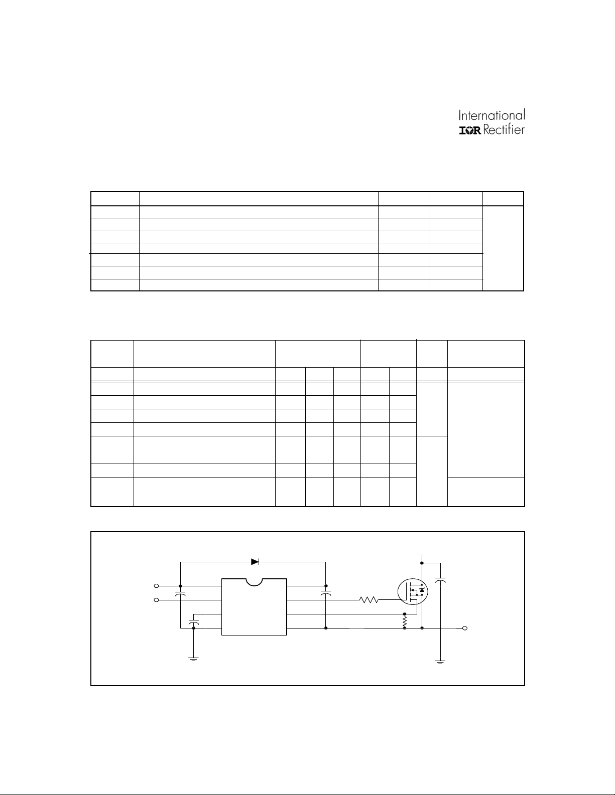
Figure 1. Input/Output Timing Diagram
50%
50%
IN
t
on
HO
Figure 3. Switching Time Waveform Definitions
t
r
10%
90%
90%
10%
t
f
t
off
< 50 V/ns
"
Figure 2. Floating Supply Voltage Transient Test Circuit
50%
CS
t
cs
OUT
Figure 4. ERR Shutdown Waveform Definitions
90%
50%
CS
t
I
dV
ERR
err
50%
1.8V
dt
1.8V
C
100 uA
50%
CS
t
cs
HO
Figure 5. CS Shutdown Waveform Definitions
90%
ERR
=× =×
dt C
Figure 6. CS to ERR Waveform Definitions
4 www.irf.com
IR2125Z
500
400
300
200
Max.
Turn-On Delay Time (ns)
Typ.
100
0
-50 -25 0 25 50 75 100 125
Temperature (°C)
500
400
300
Max.
Typ.
200
Turn-On Time (ns)
100
0
10 12 14 16 18 20
Supply Voltage (V)
V
BIAS
Figure 7A. Turn-On Time vs. Temperature Figure 7B. Turn-On Time vs. Voltage
500
400
300
200
Max.
Turn-Off Delay Time (ns)
Typ.
100
500
400
300
Max.
200
Typ.
Turn-Off Time (ns)
100
0
-50 -25 0 25 50 75 100 125
Temperature (°C)
0
10 12 14 16 18 20
Supply Voltage (V)
V
BIAS
Figure 8A. Turn-Off Time vs. Temperature Figure 8B. Turn-Off Time vs. Voltage
5.00
4.00
3.00
Max.
2.00
Typ.
1.00
ERR to Output Shutdown Delay Time (µs)
0.00
-50 -25 0 25 50 75 100 125
Temperature (°C)
Figure 9A. ERR to Output Shutdown vs. Temperature
5.00
4.00
3.00
2.00
Max.
Typ.
1.00
ERR to Output Shutdown Delay Time (µs)
0.00
10 12 14 16 18 20
Supply Voltage (V)
V
BIAS
Figure 9B. ERR to Output Shutdown vs. Voltage
www.irf.com 5

IR2125Z
100
80
60
40
Max.
Turn-On Rise Time (ns)
Typ.
20
0
-50 -25 0 25 50 75 100 125
Temperature (°C)
Figure 10A. Turn-On Rise Time vs. Temperature
100
80
60
40
Max.
Turn-Off Fall Time (ns)
Typ.
20
100
80
60
Max.
40
Typ.
Turn-On Rise Time (ns)
20
0
10 12 14 16 18 20
V
Supply Voltage (V)
BIAS
Figure 10B. Turn-On Rise Time vs. Voltage
50
40
30
20
Max.
Turn-Off Fall Time (ns)
Typ.
10
0
-50 -25 0 25 50 75 100 125
Temperature (°C)
Figure 11A. Turn-Off Fall Time vs. Temperature
15.0
12.0
Min.
9.0
6.0
Logic "1" Input Threshold (V)
3.0
0.0
-50 -25 0 25 50 75 100 125
Temperature (°C)
0
10 12 14 16 18 20
V
Supply Voltage (V)
BIAS
Figure 11B. Turn-Off Fall Time vs. Voltage
15.0
12.0
9.0
6.0
Min.
Logic "1" Input Threshold (V)
3.0
0.0
5 7.5 10 12.5 15 17.5 20
V
Logic Supply Voltage (V)
DD
Figure 12A. Logic “1” Input Threshold vs. Temperature Figure 12B. Logic “1” Input Threshold vs. Voltage
6 www.irf.com

IR2125Z
20.0
16.0
Max.
12.0
Typ.
8.0
CS to ERR Pull-Up Delay Time (µs)
4.0
0.0
-50 -25 0 25 50 75 100 125
5.00
4.00
3.00
Min.
2.00
Logic "1" Input Threshold (V)
1.00
Temperature (°C)
20.0
16.0
12.0
Max.
Typ.
8.0
CS to ERR Pull-Up Delay Time (µs)
4.0
0.0
10 12 14 16 18 20
Supply Voltage (V)
V
BIAS
Figure 13B. CS to ERR Pull-Up vs. VoltageFigure 13A. CS to ERR Pull-Up vs. T emperature
5.00
4.00
3.00
Min.
2.00
Logic "1" Input Threshold (V)
1.00
0.00
-50 -25 0 25 50 75 100 125
Temperature (°C)
Figure 14A. Logic “1” Input Threshold vs. Tempera-
0.00
10 12 14 16 18 20
Logic Supply Voltage (V)
V
CC
Figure 14B. Logic “1” Input Threshold vs. Voltage
ture
5.00
4.00
3.00
2.00
Logic "0" Input Threshold (V)
Max.
1.00
0.00
-50 -25 0 25 50 75 100 125
Temperature (°C)
Figure 15A. Logic “0” Input Threshold vs. Tempera-
5.00
4.00
3.00
2.00
Logic "0" Input Threshold (V)
Max.
1.00
0.00
10 12 14 16 18 20
Logic Supply Voltage (V)
V
CC
Figure 15B. Logic “0” Input Threshold vs. Voltage
ture
www.irf.com 7

IR2125Z
500
400
Max.
300
Typ.
200
Min.
100
CS Input Positive Going Threshold (mV)
0
-50 -25 0 25 50 75 100 125
Temperature (°C)
Figure 16A. CS Input Threshold (+) vs. Temperature
500
400
300
Max.
Typ.
200
Min.
100
CS Input Negative Going Threshold (mV)
500
400
Max.
300
Typ.
200
Min.
100
CS Input Positive Going Threshold (mV)
0
10 12 14 16 18 20
Floating Supply Voltage (V)
V
BS
Figure 16B. CS Input Threshold (+) vs. Voltage
500
400
300
Max.
Typ.
200
Min.
100
CS Input Negative Going Threshold (mV)
0
-50 -25 0 25 50 75 100 125
Temperature (°C)
Figure 17A. CS Input Threshold (-) vs. Temperature
1.00
0.80
0.60
0.40
High Level Output Voltage (V)
0.20
Max.
0.00
-50 -25 0 25 50 75 100 125
Temperature (°C)
Figure 18A. High Level Output vs. Temperature
0
10 12 14 16 18 20
Floating Supply Voltage (V)
V
BS
Figure 17B. CS Input Threshold (-) vs. Voltage
1.00
0.80
0.60
0.40
High Level Output Voltage (V)
0.20
Max.
0.00
10 12 14 16 18 20
Floating Supply Voltage (V)
V
BS
Figure 18B. High Level Output vs. Voltage
8 www.irf.com

IR2125Z
1.00
0.80
0.60
0.40
Low Level Output Voltage (V)
0.20
Max.
0.00
-50 -25 0 25 50 75 100 125
Temperature (°C)
Figure 19A. Low Level Output vs. Temperature
500
400
300
200
Offset Supply Leakage Current (µA)
100
Max.
0
-50 -25 0 25 50 75 100 125
Temperature (°C)
Figure 20A. Offset Supply Current vs. Temperature
1.00
0.80
0.60
0.40
Low Level Output Voltage (V)
0.20
Max.
0.00
10 12 14 16 18 20
Floating Supply Voltage (V)
V
BS
Figure 19B. Low Level Output vs. Voltage
500
400
300
200
Offset Supply Leakage Current (µA)
100
Max.
0
0 100 200 300 400 500
Boost Voltage (V)
V
B
Figure 20B. Offset Supply Current vs. Voltage
2.00
1.60
1.20
Max.
0.80
Supply Current (mA)
BS
V
0.40
Typ.
0.00
-50 -25 0 25 50 75 100 125
Temperature (°C)
Figure 21A. VBS Supply Current vs. Temperature
2.00
1.60
1.20
Max.
0.80
Supply Current (mA)
BS
V
0.40
Typ.
0.00
10 12 14 16 18 20
Floating Supply Voltage (V)
V
BS
Figure 21B. VBS Supply Current vs. Voltage
www.irf.com 9

IR2125Z
2.00
1.60
Max.
1.20
0.80
Supply Current (mA)
Typ.
CC
V
0.40
0.00
-50 -25 0 25 50 75 100 125
Temperature (°C)
Figure 22A. VCC Supply Current vs. Temperature
25
20
15
10
Max.
Logic "1" Input Bias Current (µA)
5
Typ.
0
-50 -25 0 25 50 75 100 125
Temperature (°C)
2.00
1.60
1.20
Max.
0.80
Supply Current (mA)
Typ.
CC
V
0.40
0.00
10 12 14 16 18 20
Figure 22B. V
25
20
15
Max.
10
Logic "1" Input Bias Current (µA)
Typ.
5
0
10 12 14 16 18 20
Logic Supply Voltage (V)
V
CC
Supply Current vs. Voltage
CC
Logic Supply Voltage (V)
V
CC
Figure 23A. Logic “1” Input Current vs. Temperature Figure 23B. Logic “1” Input Current vs. Voltage
5.00
4.00
3.00
2.00
Max.
Logic "0" Input Bias Current (µA)
1.00
0.00
-50 -25 0 25 50 75 100 125
Temperature (°C)
Figure 24A. Logic “0” Input Current vs. Temperature
5.00
4.00
3.00
2.00
Max.
Logic "0" Input Bias Current (µA)
1.00
0.00
10 12 14 16 18 20
Logic Supply Voltage (V)
V
CC
Figure 24B. Logic “0” Input Current vs. Voltage
10 www.irf.com

IR2125Z
25.0
20.0
15.0
10.0
Max.
"High" CS Bias Current (µA)
Typ.
5.0
0.0
-50 -25 0 25 50 75 100 125
Temperature (°C)
25.0
20.0
15.0
Max.
10.0
Typ.
"High" CS Bias Current (µA)
5.0
0.0
10 12 14 16 18 20
Floating Supply Voltage (V)
V
BS
Figure 25A. “High” CS Bias Current vs. Temperature Figure 25B. “High” CS Bias Current vs. Voltage
5.00
4.00
3.00
2.00
"Low" CS Bias Current (µA)
Max.
1.00
5.00
4.00
3.00
2.00
"Low" CS Bias Current (µA)
Max.
1.00
0.00
-50 -25 0 25 50 75 100 125
Temperature (°C)
0.00
10 12 14 16 18 20
Floating Supply Voltage (V)
V
BS
Figure 26A. “Low” CS Bias Current vs. Temperature Figure 26B. “Low” CS Bias Current vs. Voltage
11.0
Max.
10.0
Typ.
9.0
Min.
8.0
Undervoltage Lockout + (V)
BS
V
7.0
6.0
-50 -25 0 25 50 75 100 125
Temperature (°C)
11.0
10.0
Max.
9.0
Typ.
8.0
Min.
VBS Undervoltage Lockout - (V)
7.0
6.0
-50 -25 0 25 50 75 100 125
Temperature (°C)
Figure 27. VBS Undervoltage (+) vs. Temperature Figure 28. VBS Undervoltage (-) vs. Temperature
www.irf.com 11

IR2125Z
11.0
10.0
Max.
Typ.
9.0
Min.
8.0
Undervoltage Lockout + (V)
CC
V
7.0
6.0
-50 -25 0 25 50 75 100 125
Temperature (°C)
11.0
10.0
9.0
Max.
Typ.
8.0
Undervoltage Lockout - (V)
Min.
CC
V
7.0
6.0
-50-250 255075100125
Temperature (°C)
Figure 29. VCC Undervoltage (+) vs. Temperature Figure 30. VCC Undervoltage (-) vs. Temperature
250
200
150
Max.
Typ.
100
Min.
ERR Timing Charge Current (µA)
50
250
200
150
Max.
Typ.
100
Min.
ERR Timing Charge Current (µA)
50
0
-50 -25 0 25 50 75 100 125
Temperature (°C)
0
10 12 14 16 18 20
Logic Supply Voltage (V)
V
CC
Figure 31A. ERR Timing Charge Current vs. Temperature Figure 31B. ERR Timing Charge Current vs. Voltage
25.0
20.0
Typ.
15.0
Min.
10.0
ERR Pull-Up Current (µA)
5.0
0.0
-50 -25 0 25 50 75 100 125
Temperature (°C)
25.0
20.0
15.0
Typ.
10.0
ERR Pull-Up Current (µA)
Min.
5.0
0.0
10 12 14 16 18 20
Logic Supply Voltage (V)
V
CC
Figure 32A. ERR Pull-Up Current vs. Temperature Figure 32B. ERR Pull-Up Current vs. Voltage
12 www.irf.com

IR2125Z
50
40
Typ.
30
Min.
20
ERR Pull-Down Current (µA)
10
0
-50 -25 0 25 50 75 100 125
Temperature (°C)
Figure 33A. ERR Pull-Down Current
vs.Temperature
2.50
2.00
Typ.
1.50
Min.
1.00
Output Source Current (A)
0.50
50
40
30
Typ.
20
ERR Pull-Down Current (µA)
Max.
10
0
10 12 14 16 18 20
Logic Supply Voltage (V)
V
CC
Figure 33B. ERR Pull-Down Current vs. Voltage
2.50
2.00
1.50
Typ.
1.00
Output Source Current (A)
Min.
0.50
0.00
-50 -25 0 25 50 75 100 125
Temperature (°C)
Figure 34A. Output Source Current
0.00
10 12 14 16 18 20
Floating Supply Voltage (V)
V
BS
Figure 34B. Output Source Current vs. Voltage
vs.Temperature
5.00
Typ.
4.00
3.00
Min.
2.00
Output Sink Current (A)
1.00
0.00
-50 -25 0 25 50 75 100 125
Temperature (°C)
5.00
4.00
3.00
Typ.
2.00
Output Sink Current (A)
Min.
1.00
0.00
10 12 14 16 18 20
Floating Supply Voltage (V)
V
BS
Figure 35A. Output Sink Current vs.Temperature Figure 35B. Output Sink Current vs. Voltage
www.irf.com 13

IR2125Z
g
g
500
400
300
200
Turn-On Time (ns)
Typ.
100
0
5 7.5 10 12.5 15
Input Volta
e (V)
= 15V
V
CC
500
400
300
200
Typ.
Turn-Off Time (ns)
100
0
5 7.5 10 12.5 15
Input Volta
e (V)
Figure 36A. Turn-On Time vs. Input Voltage Figure 36B. Turn-Off Time vs. Input Voltage
0.00
-3.00
Typ.
-6.00
-9.00
Offset Supply Voltage (V)
S
V
-12.00
= 15V
V
CC
-15.00
10 12 14 16 18 20
Floating Supply Voltage (V)
V
BS
Figure 37. Maximum VS Negative Offset vs. Supply
Voltage
14 www.irf.com

Functional Block Diagram
V
CC
UV
DETECT
IN
LATCHED
SHUTDOWN
ERROR
TIMING
ERR
COM
1.8V
1.8V
PULSE
GEN
Q R
UP
SHIFTERS
S
LEVEL
SHIFT
PULSE
FILTER
IR2125Z
V
B
UV
DETECT
R
R
S
DOWN
SHIFTERS
HV
PULSE
FILTER
V
B
HV
LEVEL
SHIFT
Q
PULSE
GEN
PRE
DRIVER
500ns
BLANK
BUFFER
0.23V
-
+
AMPLIFER
COMPARATOR
HO
V
S
CS
Lead Definitions
Symbol Description
V
CC
IN Logic input for gate driver output (HO), in phase with HO
ERR Serves multiple functions; status reporting, linear mode timing and cycle by cycle logic
COM Logic ground
V
B
HO
V
S
CS
www.irf.com 15
Logic and gate drive supply
shutdown
High side floating supply
High side gate drive output
High side floating supply return
Current sense input to current sense comparator

IR2125Z
Case Outline and Dimensions- MO-036AA
IR2125Z
IR2153Z
IR WORLD HEADQUARTERS: 233 Kansas St., El Segundo, California 90245, USA Tel: (310) 252-7105
TAC Fax: (310) 252-7903
Visit us at www.irf.com for sales contact information.
Data and specifications subject to change without notice. 05/01
16 www.irf.com
 Loading...