International Rectifier ST180S04M0L, ST180S04M0, ST180S20P1L, ST180S20P1, ST180S20P0L Datasheet
...
DISCRETE POWER DIODES and THYRISTORS
Next Data SheetIndex
Previous Datasheet
To Order
DATA BOOK

Bulletin I25165/B
Next Data SheetIndex
Previous Datasheet
To Order
ST180S SERIES
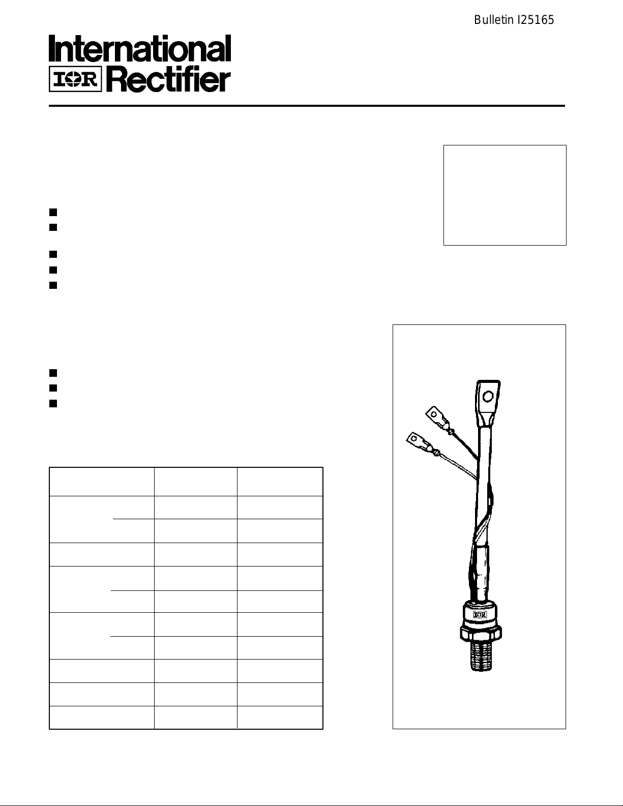
PHASE CONTROL THYRISTORS Stud Version
Features
Center amplifying gate
Hermetic metal case with ceramic insulator
(Also available with glass-metal seal up to 1200V)
International standard case TO-209AB (TO-93)
Threaded studs UNF 3/4 - 16UNF2A or ISO M16x1.5
Compression Bonded Encapsulation for heavy duty
operations such as severe thermal cycling
Typical Applications
DC motor controls
Controlled DC power supplies
AC controllers
Major Ratings and Characteristics
Parameters ST180S Units
200A
I
T(AV)
@ T
C
I
T(RMS)
I
TSM
2
I
t @ 50Hz 125 KA2s
V
DRM/VRRM
t
q
T
J
@ 50Hz 5000 A
@ 60Hz 5230 A
@ 60Hz 114 KA
typical 100 µs
200 A
85 °C
314 A
400 to 2000 V
- 40 to 125 °C
2
s
case style
TO-209AB (TO-93)

ST180S Series
=
, Gate 0V 100Ω,
= 500µs
To Order
Next Data SheetIndex
Previous Datasheet
ELECTRICAL SPECIFICATIONS
Voltage Ratings
Voltage V
DRM/VRRM
Type number Code peak and off-state voltage repetitive peak voltage
, max. repetitive V
, maximum non- I
RSM
DRM/IRRM
@ TJ = TJ max
V V mA
04 400 500
08 800 900
ST180S 30
12 1200 1300
16 1600 1700
18 1800 1900
20 2000 2100
On-state Conduction
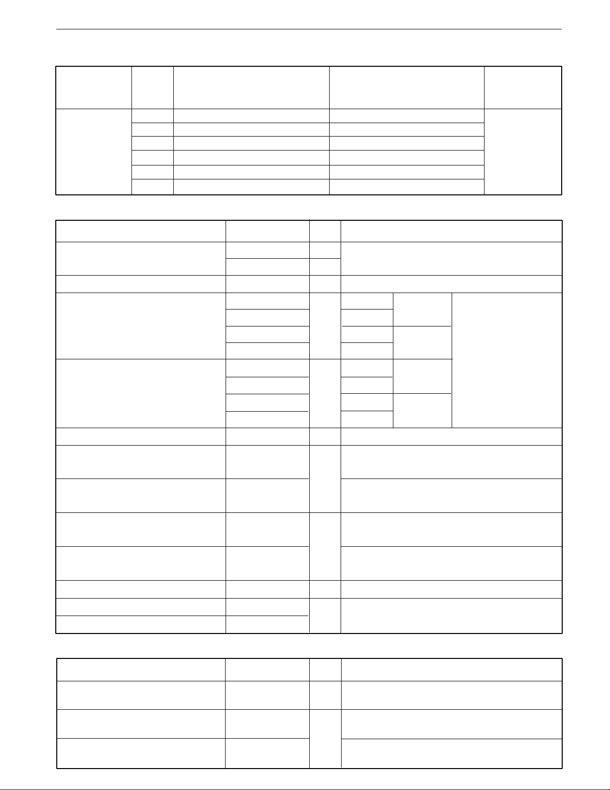
Parameter ST180S Units Conditions
I
T(AV)
I
T(RMS)
I
TSM
2
I
2
I
Max. average on-state current 200 A 180° conduction, half sine wave
@ Case temperature 85 °C
Max. RMS on-state current 314 A DC @ 76°C case temperature
Max. peak, one-cycle 5000 t = 10ms No voltage
non-repetitive surge current 5230 t = 8.3ms reapplied
4200 t = 10ms 100% V
A
RRM
4400 t = 8.3ms reapplied Sinusoidal half wave,
t Maximum I2t for fusing 125 t = 10ms No voltage Initial TJ = TJ max.
114 t = 8.3ms reapplied
KA2s
88 t = 10ms 100% V
RRM
81 t = 8.3ms reapplied
√t Maximum I2√t for fusing 1250 KA2√s t = 0.1 to 10ms, no voltage reapplied
max.
12
V
Low level value of threshold
T(TO)1
voltage
V
High level value of threshold
T(TO)
2
voltage
r
t1
Low level value of on-state
slope resistance
r
t2
High level value of on-state
slope resistance
V
I
H
I
L
Max. on-state voltage 1.75 V Ipk= 570A, TJ = 125°C, tp = 10ms sine pulse
TM
Maximum holding current 600
Max. (typical) latching current 1000 (300)
Switching
Parameter ST180S Units Conditions
di/dt Max. non-repetitive rate of rise Gate drive 20V, 20Ω, tr ≤ 1µs
of turned-on current T
t
d
Typical delay time 1.0
t
q
Typical turn-off time 100
1.08 (16.7% x π x I
V
1.14 (I > π x I
T(AV)
1.18 (16.7% x π x I
mΩ
1.14 (I > π x I
mA T
1000 A/µs
J
T(AV)
= TJ max, anode supply 12V resistive load
J
= TJ max, anode voltage ≤ 80% V
Gate current 1A, dig/dt = 1A/µs
V
= 0.67% V
d
µs
I
= 300A, TJ = TJ max, di/dt = 20A/µs, VR = 50V
TM
dv/dt
20V/µs
< I < π x I
T(AV)
),TJ = TJ max.
< I < π x I
T(AV)
),TJ = TJ max.
= 25°C
DRM, TJ
), TJ = TJ max.
T(AV)
), TJ = TJ max.
T(AV)
DRM
t
p
2222222222222
 Loading...