International Rectifier IRU1205CL, IRU1205-36CL, IRU1205-33CL, IRU1205-30CL, IRU1205-28CL Datasheet
...
Data Sheet No. PD94133
IRU1205 / IRU1205-25 / IRU1205-28
IRU1205-30 / IRU1205-33 / IRU1205-36
300mA ULTRA LOW DROPOUT POSITIVE
ADJUSTABLE AND FIXED REGULATORS
FEATURES
SOT-23 Package
Stable with 2.2µF Ceramic Capacitor
1% Voltage Reference Accuracy
Only 270mV Dropout at 300mA
and 170mV Dropout at 150mA
5µA Quiescent Current in Shutdown
Current Limit and Thermal Shutdown
Logic Input Enable Pin
APPLICATIONS
Laptop, Notebook & Palmtop computers
Battery Powered Equipments
PCMCIA Vcc & Vpp Regulator
Consumer Electronics
High Efficiency Linear Power Supplies
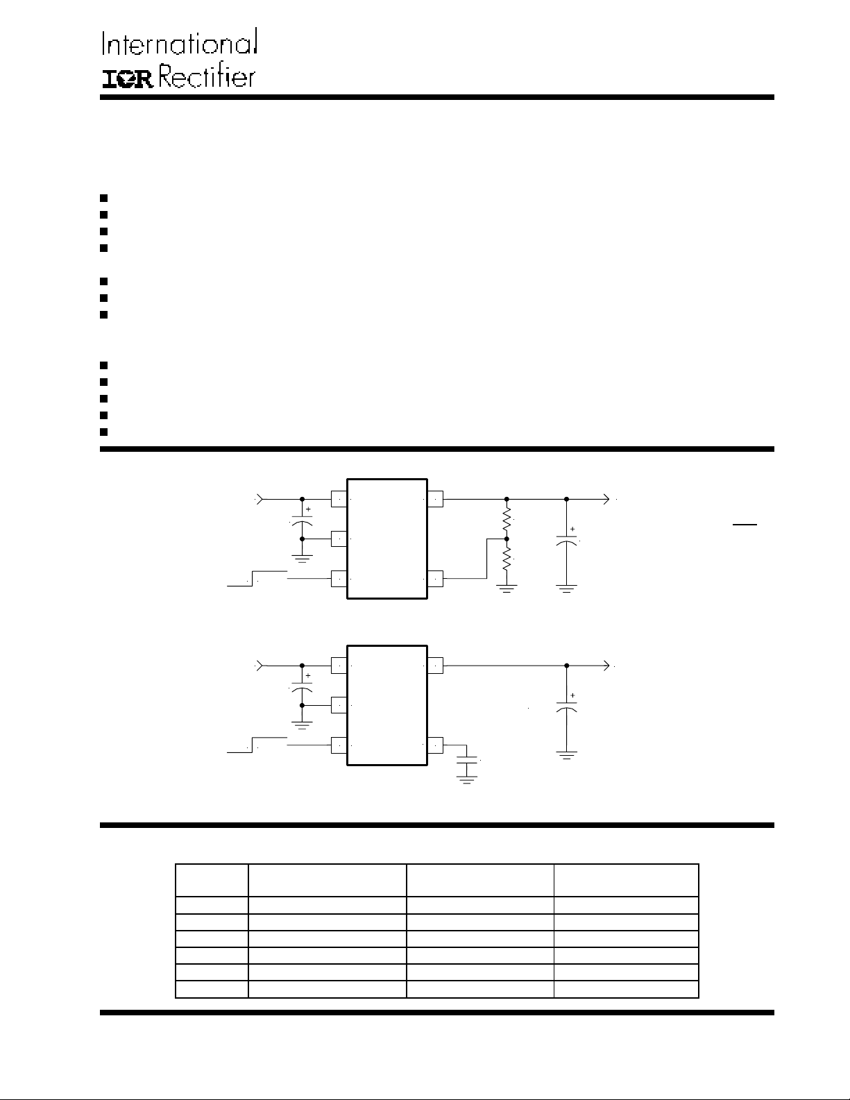
TYPICAL APPLICATION
V
IN
C1
2.2uF
SD Enable
V
V
IN
1
Gnd
2
En
3 4
OUT
Adj
DESCRIPTION
The IRU1205 device is an efficient linear voltage regulator with better than 1% initial voltage accuracy, very low
dropout voltage and very low ground current designed
especially for hand held, battery powered applications.
Other features of the device are: TTL compatible enable/
shutdown control input, current limiting and thermal shutdown.
The IRU1205 is available in fixed and adjustable output
voltage versions in a small SOT-23, 5-Pin package.
C2
2.2uF
V
OUT
Vo = 1.242 ×
oo
o1+
oo
5
R1
R2
R1
R2
pp
p
pp
Figure 1 - Typical application of the IRU1205 ajustable voltage regulator.
V
3.3V
SD Enable
C1
2.2uF
V
IN
1
Gnd
2
En
3 4
OUT
5
C
BYP
Figure 2 - Typical application of the IRU1205-25 fixed voltage regulator.
PACKAGE ORDER INFORMATION
TJ (°C) 5-PIN SOT-23 OUTPUT
SOT-23 (L5) MARKING VOLTAGE
0 To 125 IRU1205CL AT00 Adj
0 To 125 IRU1205-25CL AT25 2.5V
0 To 125 IRU1205-28CL AT28 2.8V
0 To 125 IRU1205-30CL AT30 3.0V
0 To 125 IRU1205-33CL AT33 3.3V
0 To 125 IRU1205-36CL AT36 3.6V
2.5V
C2
2.2uF
C3
1000pF
Rev. 2.0
02/15/02
www.irf.com
1

IRU1205 / IRU1205-25 / IRU1205-28
IRU1205-30 / IRU1205-33 / IRU1205-36
ABSOLUTE MAXIMUM RATINGS
Input Voltage (VIN) ..................................................... 10V
Enable Input Voltage ................................................. 10V
Storage Temperature Range ....................................... -65°C To 150°C
Operating Junction Temperature Range ...................... 0°C To 150°C
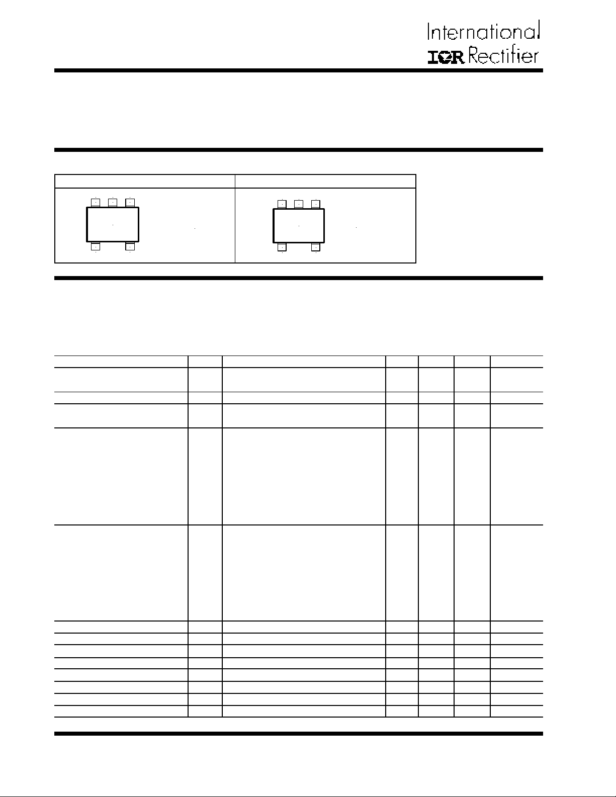
PACKAGE INFORMATION
5-PIN SOT-23 (L5) 5-PIN SOT-23 (L5)
Gnd V
IN
En
Gnd V
3 2 1
IN
En
3 2 1
AT00
4 5
Adj
OUT
V
Adjustable
θJA=256&C/W
ATxx
4 5
C
BYP
Fixed
OUT
θJA=256&C/W
V
ELECTRICAL SPECIFICATIONS
Unless otherwise specified, these specifications apply over CIN=Co=22µF, Io=100µA, VIN(MIN)=2.5V(Adjustable
devices) VIN=Vo + 1V(for fixed voltage devices), VOUT=VFB(for adjustable version only), CBYP=470pF(for AT25, AT28,
AT30, AT33 and AT36), VENB=2V and TA=25&C. Typical values refer to TA=25&C. Low duty cycle pulse testing is used
which keeps junction and case temperatures equal to the ambient temperature.
PARAMETER SYM TEST CONDITION MIN TYP MAX UNITS
Reference Voltage Vo -1 1 %
(See Table 1 for typical values) (Note 4) -2 2
Line Regulation ∆VI Vo + 1V<VIN<10V 0.005 %/V
Load Regulation (Note 1) ∆VL 1mA<Io<100mA 0.8 %
100mA<Io<300mA 0.1
Dropout Voltage (Note 2) ∆VI(O) Io=100µA 10 50 mV
Io=100µA (Note 4) 13 70
Io=50mA 85 110
Io=50mA (Note 4) 100 140
Io=150mA 170 220
Io=150mA (Note 4) 204 260
Io=300mA 270 350
Io=300mA (Note 4) 324 400
Ground Current (Note 3) IQ VEN=2V, Io=100µA 120 160 µA
Io=100µA (Note 4) 240
Io=50mA 420 600
Io=50mA (Note 4) 540
Io=150mA 2200 2900
Io=150mA (Note 4) 2900
Io=300mA 7200 9500
Io=300mA (Note 4) 9300
Ground Current-SD Activated IQ(SD) VEN=0V to 0.8V or Open 5 µA
Current Limit ICL Vo=0V 320 420 mA
Thermal Regulation ∆VP VIN=10V, Io=150mA,10ms Pulse 0.05 %/W
Adjust Pin Current IADJ VIN=2.5V, Vo=VADJ 0.1 µA
Enable Pin Input LO Voltage VEN(L) Regulator OFF 0.8 V
Enable Pin Input HI Voltage VEN(H) Regulator ON 2 V
Enable Pin Input LO Current VEN(L)=0V to 0.8V 0.01 µA
Enable Pin Input HI Current VEN(H)=2V to VIN 20 µA
2
www.irf.com
Rev. 2.0
02/15/02
 Loading...