International Rectifier IRU1117-33CY, IRU1117-33CS, IRU1117-33CP, IRU1117-33CD Datasheet

Data Sheet No. PD94172
IRU1117-33
800mA LOW DROPOUT POSITIVE
FIXED 3.3V REGULATOR
FEATURES
Guaranteed < 1.2V Dropout at 800mA Load
Current
Fast Transient Response
1% Output Voltage Initial Accuracy
Built-In Thermal Shutdown
Available in SOT-223, D-Pak, Ultra Thin-Pak
and 8-Pin SOIC Surface-Mount Packages
APPLICATIONS
VGA & Sound Card Applications
Standard 3.3V Chip Set and Logic Applications
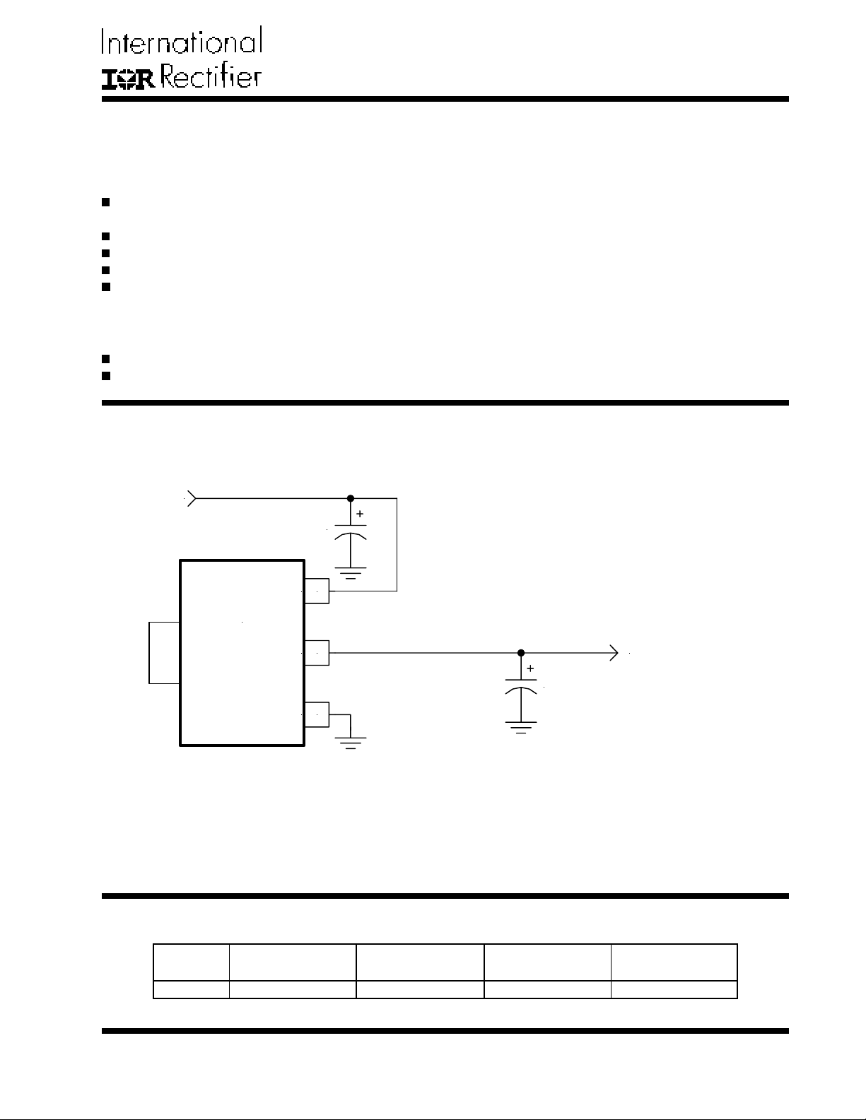
TYPICAL APPLICATION
5V
C1
10uF
DESCRIPTION
The IRU1117-33 is a low dropout three-terminal fixed output regulator with minimum of 800mA output current capability. This product is specifically designed to provide
well regulated supply for low voltage IC applications such
as VGA, sound & DVD cards. The IRU1117-33 is guaranteed to have <1.2V dropout at full load current making
it ideal to provide well regulated with 4.75V to 7V input
supply. The IRU1117-33 is specifically designed to be
stable with low cost aluminum capacitors while maintaining stability with low ESR tantalum caps.
Vin
3
IRU1117-33
Vout
2
Gnd
1
Figure 1 - Typical application of IRU1117-33 in a 5V to 3.3V regulator
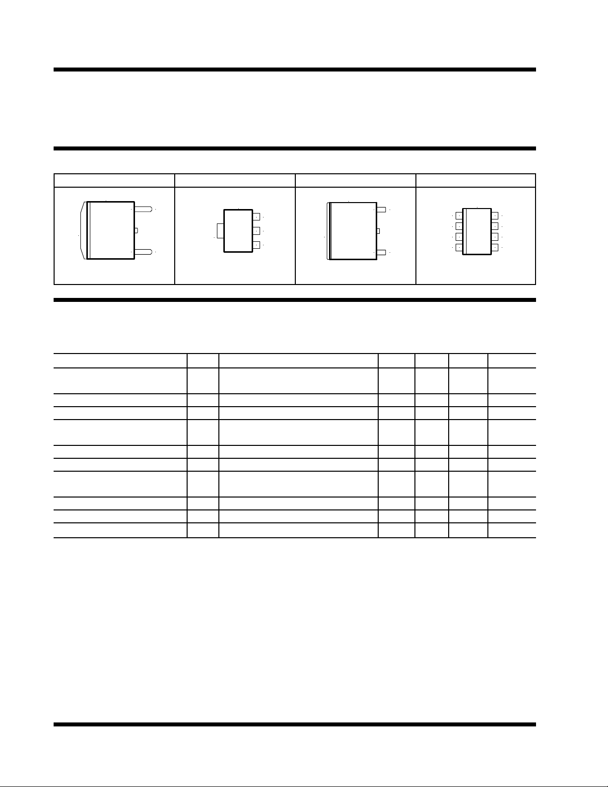
PACKAGE ORDER INFORMATION
Tj (°C) 2-PIN PLASTIC 3-PIN PLASTIC 2-PIN PLASTIC 8-PIN PLASTIC
TO-252 (D-Pak) SOT-223 (Y) Ultra Thin-Pak (P) SOIC (S)
0 To 150 IRU1117-33CD IRU1117-33CY IRU1117-33CP IRU1117-33CS
3.3V / 800mA
C2
10uF
Rev. 1.3
06/29/01
1

IRU1117-33
ABSOLUTE MAXIMUM RATINGS
Input Voltage (Vin) .................................................... 7V
Power Dissipation ..................................................... Internally Limited
Storage Temperature Range ...................................... -65°C To 150°C
Operating Junction Temperature Range ..................... 0°C To 150°C
PACKAGE INFORMATION
2-PIN PLASTIC TO-252 (D-Pak) 3-PIN PLASTIC SOT-223 (Y) 2-PIN ULTRA THIN-PAK (P) 8-PIN PLASTIC SOIC (S)
Tab is
Vout
FRONT VIEW
3
Vin
1
Gnd
Tab i s
Vou t
TOP VIEW
3
Vin
2
Vou t
1
Gnd
θJA=70°C/W for 0.5" Sq pad θJA=90°C/W for 0.4" Sq pad θJA=70°C/W for 0.5" Sq pad θJA=55°C/W for 1" Sq pad
ELECTRICAL SPECIFICATIONS
Unless otherwise specified, these specifications apply over Cin=1µF, Vin=5V, Cout=10µF, and Tj=0 to 125!C.
Typical values refer to Tj=25!C.
Tab is
Vout
FRONT VIEW
3
Vin
1
Gnd
Vin
NC
NC
TOP VIEW
1
2
3
4
8
Vout
7
Vout
6
Vout
5
VoutGnd
PARAMETER SYM TEST CONDITION MIN TYP MAX UNITS
Output Voltage Vo Io=10mA,Tj=25!C 3.267 3.300 3.333 V
Io=10mA 3.235 3.300 3.365
Line Regulation Io=10mA, 4.75V<Vin<7V 7 mV
Load Regulation (Note 1) 10mA<Io<800mA 17 mV
Dropout Voltage (Note 2) Io=1A 1.3
Io=800mA 1.2 V
Current Limit dVo=100mV 1.1 A
Thermal Regulation 30ms Pulse, Io=800mA 0.01 0.02 %/W
Ripple Rejection f=120Hz, Co=25µF Tantalum,
Io=0.5A 60 70 dB
Temperature Stability Io=10mA 0.5 %
Long Term Stability Tj=125!C, 1000Hrs 0.3 1 %
RMS Output Noise Tj=25!C, 10Hz<f<10KHz 0.003 %Vo
Note 1: Low duty cycle pulse testing with Kelvin connections is required in order to maintain accurate data.
Note 2: Dropout voltage is defined as the minimum differential voltage between Vin and Vout required to maintain
regulation at Vout. It is measured when the output voltage drops 1% below its nominal value.
2
Rev. 1.3
06/29/01
 Loading...