

International Rectifier IRFPS40N50L Datasheet
PD- 93923B
SMPS MOSFET
Applications
l Switch Mode Power Supply (SMPS)
l UninterruptIble Power Supply
l High Speed Power Switching
l ZVS and High Frequency Circuit
l PWM Inverters
V
500V 0.087Ω 46A
IRFPS40N50L
HEXFET® Power MOSFET
DSS
R
DS(on)
typ. I
Benefits
l Low Gate Charge Qg results in Simple Drive Requirement
l Improved Gate, Avalanche and Dynamicdv/dt
Ruggedness
l Fully Characterized Capacitance and Avalanche Voltage
and Current
l Low Trr and Soft Diode Recovery
l High Performance Optimised Anti-parallel Diode
SUPER TO-247AC
Absolute Maximum Ratings
Parameter Max. Units
ID @ TC = 25°C Continuous Drain Current, VGS @ 10V 46
ID @ TC = 100°C Continuous Drain Current, VGS @ 10V 29 A
I
DM
PD @TC = 25°C Power Dissipation 540 W
V
GS
T
J
T
STG
Pulsed Drain Current 180
Linear Derating Factor 4.3 W/°C
Gate-to-Source Voltage ± 30 V
dv/dtPeak Diode Recovery dv/dt 25 V/ns
Operating Junction and -55 to + 150
Storage Temperature Range
Soldering Temperature, for 10 seconds 300
(1.6mm from case )
°C
Diode Characteristics
Symbol Parameter Min. Typ. Max. Units Conditions
I
S
I
SM
V
t
rr
Q
I
RRM
t
on
SD
rr
Continuous Source Current ––– ––– 46 MOSFET symbol
(Body Diode) showing the
Pulsed Source Current ––– ––– 180 integral reverse
(Body Diode) p-n junction diode.
Diode Forward Voltage ––– ––– 1.5 V TJ = 25°C, IS = 46A, VGS = 0V
Reverse Recovery Time
Reverse Recovery Charge
Reverse Recovery Current ––– 9.0 ––– A
Forward Turn-On Time Intrinsic turn-on time is negligible (turn-on is dominated by LS+LD)
––– 170 250 TJ = 25°C I
––– 220 330 TJ = 125°C di/dt = 100A/µs
––– 705 1060 nC TJ = 25°C
––– 1.3 2.0 µCTJ = 125°C
ns
A
= 46A
F
G
Typical SMPS Topologies
l Bridge Converters l All Zero Voltage Switching
www.irf.com 1
D
D
S
05/09/01
IRFPS40N50L
Static @ TJ = 25°C (unless otherwise specified)
Symbol Parameter Min. Typ. Max. Units Conditions
V
(BR)DSS
∆V
(BR)DSS
R
DS(on)
V
GS(th)
I
DSS
I
GSS
Dynamic @ TJ = 25°C (unless otherwise specified)
Symbol Parameter Min. Typ. Max. Units Conditions
g
fs
Q
g
Q
gs
Q
gd
t
d(on)
t
r
t
d(off)
t
f
C
iss
C
oss
C
rss
C
oss
C
oss
C
eff. Effective Output Capacitance ––– 420 ––– VGS = 0V, VDS = 0V to 400V
oss
Drain-to-Source Breakdown Voltage 500 ––– ––– VVGS = 0V, ID = 250µA
/∆T
Breakdown Voltage Temp. Coefficient ––– 0.60 ––– V/°C Reference to 25°C, ID = 1mA
J
Static Drain-to-Source On-Resistance ––– 0.087 0.100 Ω VGS = 10V, ID = 28A
Gate Threshold Voltage 3.0 ––– 5.0 V VDS = VGS, ID = 250µA
Drain-to-Source Leakage Current
Gate-to-Source Forward Leakage ––– ––– 100 VGS = 30V
Gate-to-Source Reverse Leakage ––– ––– -100
––– ––– 50 µA V
––– ––– 2.0 mA VDS = 400V, VGS = 0V, TJ = 125°C
nA
= 500V, VGS = 0V
DS
VGS = -30V
Forward Transconductance 21 ––– ––– SVDS = 50V, ID = 46A
Total Gate Charge ––– ––– 380 ID = 46A
Gate-to-Source Charge ––– ––– 80 nC VDS = 400V
Gate-to-Drain ("Miller") Charge ––– ––– 190 VGS = 10V, See Fig. 6 and 13
Turn-On Delay Time ––– 27 ––– VDD = 250V
Rise Time ––– 170 ––– ID = 46A
Turn-Off Delay Time ––– 50 ––– RG = 0.85Ω
ns
Fall Time ––– 69 ––– VGS = 10V,See Fig. 10
Input Capacitance ––– 8110 ––– VGS = 0V
Output Capacitance ––– 960 ––– VDS = 25V
Reverse Transfer Capacitance ––– 130 ––– pF ƒ = 1.0MHz, See Fig. 5
Output Capacitance ––– 11200 ––– VGS = 0V, VDS = 1.0V, ƒ = 1.0MHz
Output Capacitance ––– 240 ––– VGS = 0V, VDS = 400V, ƒ = 1.0MHz
Avalanche Characteristics
Symbol Parameter Typ. Max. Units
E
AS
I
AR
E
AR
Single Pulse Avalanche Energy ––– 920 mJ
Avalanche Current ––– 46 A
Repetitive Avalanche Energy ––– 54 mJ
Thermal Resistance
Symbol Parameter Typ. Max. Units
R
θJC
R
θCS
R
θJA
Notes:
Repetitive rating; pulse width limited by
max. junction temperature. (See Fig. 11)
Starting T
I
= 46A (See Figure 12a)
AS
I
≤ 46A, di/dt ≤ 367A/µs, V
SD
TJ ≤ 150°C.
Junction-to-Case ––– 0.23
Case-to-Sink, Flat, Greased Surface 0.24 ––– °C/W
Junction-to-Ambient ––– 40
Pulse width ≤ 400µs; duty cycle ≤ 2%.
C
eff. is a fixed capacitance that gives the same charging time
= 25°C, L = 0.86mH, RG = 25Ω,
J
≤ V
DD
(BR)DSS
,
oss
as C
oss
while V
is rising from 0 to 80% V
DS
DSS
2 www.irf.com
IRFPS40N50L
1000
100
10
1
0.1
D
I , Drain-to-Source Current (A)
0.01
0.1 1 10 100
1000
VGS
TOP
15V
10V
8.0V
7.0V
6.0V
5.5V
5.0V
BOTTOM
4.5V
20µs PULSE WIDTH
T = 25 C
J
V , Drain-to-Source Voltage (V)
DS
4.5V
°
1000
100
10
1
D
I , Drain-to-Source Current (A)
0.1
0.1 1 10 100
VGS
TOP
15V
10V
8.0V
7.0V
6.0V
5.5V
5.0V
BOTTOM
4.5V
20µs PULSE WIDTH
T = 150 C
J
V , Drain-to-Source Voltage (V)
DS
4.5V
°
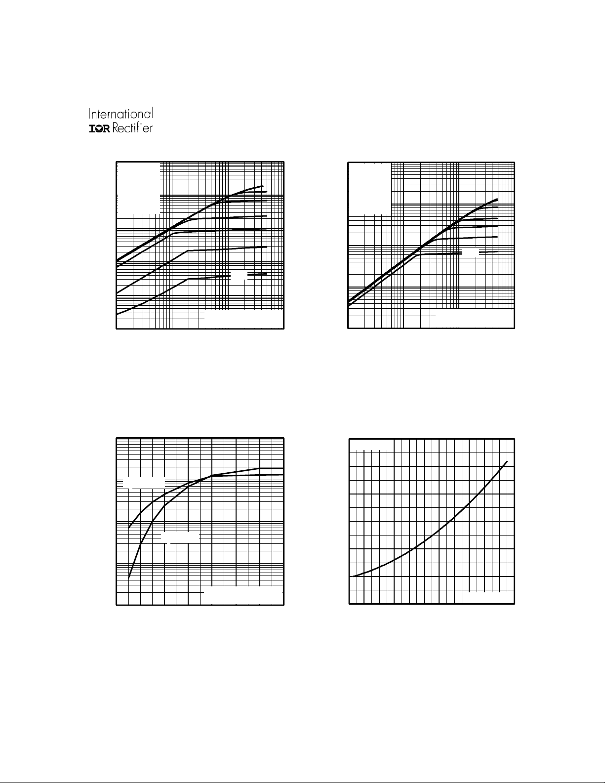
Fig 2. Typical Output CharacteristicsFig 1. Typical Output Characteristics
3.0
47A
I =
D
2.5
100
10
1
D
I , Drain-to-Source Current (A)
0.1
4 5 6 7 8 9 10 11
Fig 3. Typical Transfer Characteristics
°
T = 150 C
J
°
T = 25 C
J
V = 50V
DS
20µs PULSE WIDTH
V , Gate-to-Source Voltage (V)
GS
2.0
1.5
(Normalized)
1.0
0.5
DS(on)
R , Drain-to-Source On Resistance
0.0
-60 -40 -20 0 20 40 60 80 100 120 140 160
T , Junction Temperature ( C)
J
V =
Fig 4. Normalized On-Resistance
GS
10V
°
Vs. Temperature
www.irf.com 3
 Loading...