

International Rectifier IRFPC50A Datasheet
TO-247AC
PD- 91898
SMPS MOSFET
IRFPC50A
HEXFET® Power MOSFET
Applications
l Switch Mode Power Supply ( SMPS )
l Uninterruptable Power Supply
l High speed power switching
Benefits
l Low Gate Charge Qg results in Simple
Drive Requirement
l Improved Gate, Avalanche and dynamic
dv/dt Ruggedness
l Fully Characterized Capacitance and
Avalanche Voltage and Current
l Effective Coss specified ( See AN 1001)
Absolute Maximum Ratings
Parameter Max. Units
ID @ TC = 25°C Continuous Drain Current, VGS @ 10V 11
ID @ TC = 100°C Continuous Drain Current, VGS @ 10V 7.0 A
I
DM
PD @TC = 25°C Power Dissipation 180 W
V
GS
dv/dt Peak Diode Recovery dv/dt 4.9 V/ns
T
J
T
STG
Pulsed Drain Current 44
Linear Derating Factor 1.4 W/°C
Gate-to-Source Voltage ± 30 V
Operating Junction and -55 to + 150
Storage Temperature Range
Soldering Temperature, for 10 seconds 300 (1.6mm from case )
Mounting torqe, 6-32 or M3 screw 10 lbf•in (1.1N•m)
V
DSS
Rds(on) max I
600V 0.58Ω 11A
SDG
D
°C
Typical SMPS Topology:
l PFC Boost
Notes through are on page 8
www.irf.com 1
6/23/99
IRFPC50A
Static @ TJ = 25°C (unless otherwise specified)
Parameter Min. Typ. Max. Units Conditions
V
(BR)DSS
∆V
(BR)DSS
R
DS(on)
V
GS(th)
I
DSS
I
GSS
Dynamic @ TJ = 25°C (unless otherwise specified)
g
fs
Q
g
Q
gs
Q
gd
t
d(on)
t
r
t
d(off)
t
f
C
iss
C
oss
C
rss
C
oss
C
oss
C
eff. Effective Output Capacitance ––– 81 ––– VGS = 0V, VDS = 0V to 480V
oss
Avalanche Characteristics
E
AS
I
AR
E
AR
Thermal Resistance
R
θJC
R
θCS
R
θJA
Diode Characteristics
I
S
I
SM
V
SD
t
rr
Q
rr
t
on
2 www.irf.com
Drain-to-Source Breakdown Voltage 600 ––– ––– V VGS = 0V, ID = 250µA
/∆T
Breakdown Voltage Temp. Coefficient
J
––– 0.65 ––– V/°C Reference to 25°C, ID = 1mA
Static Drain-to-Source On-Resistance ––– ––– 0.58 Ω VGS = 10V, ID = 6.0A
Gate Threshold Voltage 2.0 ––– 4. 0 V VDS = VGS, ID = 250µA
Drain-to-Source Leakage Current
––– ––– 25
––– ––– 250 VDS = 480V, VGS = 0V, TJ = 125°C
Gate-to-Source Forward Leakage ––– ––– 100 VGS = 30V
Gate-to-Source Reverse Leakage ––– ––– -100
VDS = 600V, VGS = 0V
µA
nA
VGS = -30V
Parameter Min. Typ. Max. Units Conditions
Forward Transconductance 7.7 ––– ––– S VDS = 50V, ID = 6.0A
Total Gate Charge ––– ––– 70 ID = 11A
Gate-to-Source Charge ––– ––– 19 nC VDS = 480V
Gate-to-Drain ("Miller") Charge ––– ––– 28 VGS = 10V, See Fig. 6 and 13
Turn-On Delay Time ––– 15 ––– VDD = 300V
Rise Time ––– 40 ––– ID = 11A
Turn-Off Delay Time ––– 33 ––– RG = 6.2Ω
ns
Fall Time ––– 29 ––– RD = 30Ω,See Fig. 10
Input Capacitance ––– 2100 ––– VGS = 0V
Output Capacitance ––– 270 ––– VDS = 25V
Reverse Transfer Capacitance ––– 9.7 ––– pF ƒ = 1.0MHz, See Fig. 5
Output Capacitance ––– 2830 ––– VGS = 0V, VDS = 1.0V, ƒ = 1.0MHz
Output Capacitance ––– 74 ––– VGS = 0V, VDS = 480V, ƒ = 1.0MHz
Parameter Typ. Max. Units
Single Pulse Avalanche Energy ––– 920 mJ
Avalanche Current ––– 11 A
Repetitive Avalanche Energy ––– 18 mJ
Parameter Typ. Max. Units
Junction-to-Case ––– 0.65
Case-to-Sink, Flat, Greased Surface 0.24 ––– °C/W
Junction-to-Ambient ––– 40
Parameter Min. Typ. Max. Units Conditions
Continuous Source Current MOSFET symbol
(Body Diode)
Pulsed Source Current integral reverse
(Body Diode)
––– –––
––– –––
Diode Forward Voltage ––– ––– 1.4 V TJ = 25°C, IS = 11A, VGS = 0V
Reverse Recovery Time ––– 500 740 ns TJ = 25°C, IF = 11A
Reverse RecoveryCharge ––– 4.0 6 .0 µC di/dt = 100A/µs
Forward Turn-On Time Intrinsic turn-on time is negligible (turn-on is dominated by LS+LD)
11
44
showing the
A
p-n junction diode.
G
D
S
IRFPC50A
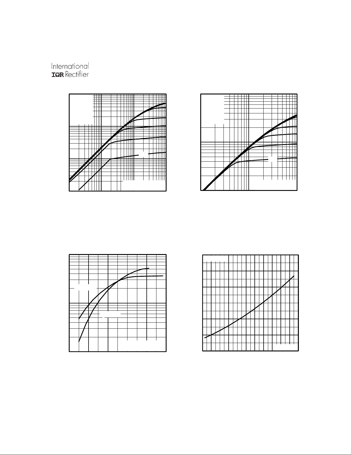
100
10
TOP
BOTTOM
VGS
15V
10V
8.0V
7.0V
6.0V
5.5V
5.0V
4.5V
4.5V
1
D
I , Drain-to-Source Current (A)
20µs PULSE WIDTH
°
T = 25 C
0.1
0.1 1 10 100
V , Drain-to-Source Voltage (V)
DS
100
J
100
10
TOP
BOTTOM
VGS
15V
10V
8.0V
7.0V
6.0V
5.5V
5.0V
4.5V
4.5V
D
I , Drain-to-Source Current (A)
20µs PULSE WIDTH
°
T = 150 C
1
1 10 100
V , Drain-to-Source Voltage (V)
DS
J
Fig 2. Typical Output CharacteristicsFig 1. Typical Output Characteristics
3.0
I =
D
11A
13A
2.5
°
T = 150 C
J
10
°
T = 25 C
J
D
I , Drain-to-Source Current (A)
100V
V = 50V
DS
1
4.0 5.0 6.0 7.0 8.0 9.0
V , Gate-to-Source Voltage (V)
GS
20µs PULSE WIDTH
Fig 3. Typical Transfer Characteristics
2.0
1.5
(Normalized)
1.0
0.5
DS(on)
R , Drain-to-Source On Resistance
0.0
-60 -40 -20 0 20 40 60 80 100 120 140 160
T , Junction Temperature ( C)
J
Fig 4. Normalized On-Resistance
V =
GS
°
10V
Vs. Temperature
www.irf.com 3
 Loading...