

International Rectifier IRFP90N20D Datasheet
SMPS MOSFET
PD - 94301A
IRFP90N20D
HEXFET® Power MOSFET
Applications
l High frequency DC-DC converters
V
DSS
R
DS(on)
max I
200V 0.023Ω 94A
Benefits
l Low Gate-to-Drain Charge to Reduce
Switching Losses
l Fully Characterized Capacitance Including
Effective C
to Simplify Design, (See
OSS
App. Note AN1001)
l Fully Characterized Avalanche Voltage
and Current
TO-247AC
Absolute Maximum Ratings
Parameter Max. Units
ID @ TC = 25°C Continuous Drain Current, VGS @ 10V 94o
ID @ TC = 100°C Continuous Drain Current, VGS @ 10V 66 A
I
DM
PD @TC = 25°C Power Dissipation 580 W
V
GS
dv/dt Peak Diode Recovery dv/dt 6.7 V/ns
T
J
T
STG
Pulsed Drain Current 380
Linear Derating Factor 3.8 W/°C
Gate-to-Source Voltage ± 30 V
Operating Junction and -55 to + 175
Storage Temperature Range
Soldering Temperature, for 10 seconds 300 (1.6mm from case )
Mounting torqe, 6-32 or M3 screw 10 lbf•in (1.1N•m)
D
o
°C
Thermal Resistance
Parameter Typ. Max. Units
R
θJC
R
θCS
R
θJA
Notes through o are on page 8
Junction-to-Case ––– 0.26
Case-to-Sink, Flat, Greased Surface 0.24 ––– °C/W
Junction-to-Ambient ––– 40
www.irf.com 1
09/27/01
IRFP90N20D
Static @ TJ = 25°C (unless otherwise specified)
Parameter Min. Typ. Max. Units Conditions
V
(BR)DSS
∆V
(BR)DSS
R
DS(on)
V
GS(th)
I
DSS
I
GSS
Dynamic @ TJ = 25°C (unless otherwise specified)
g
fs
Q
g
Q
gs
Q
gd
t
d(on)
t
r
t
d(off)
t
f
C
iss
C
oss
C
rss
C
oss
C
oss
C
eff. Effective Output Capacitance ––– 870 ––– VGS = 0V, VDS = 0V to 160V
oss
Drain-to-Source Breakdown Voltage 200 ––– ––– VVGS = 0V, ID = 250µA
/∆T
Breakdown Voltage Temp. Coefficient
J
––– 0.24 ––– V/°C Reference to 25°C, ID = 1mA
Static Drain-to-Source On-Resistance ––– ––– 0.023 Ω VGS = 10V, ID = 56A
Gate Threshold Voltage 3. 0 ––– 5.0 V VDS = VGS, ID = 250µA
Drain-to-Source Leakage Current
––– ––– 25
––– ––– 250 VDS = 160V, VGS = 0V, TJ = 150°C
Gate-to-Source Forward Leakage ––– ––– 100 VGS = 30V
Gate-to-Source Reverse Leakage ––– ––– -100
VDS = 200V, VGS = 0V
µA
nA
VGS = -30V
Parameter Min. Typ. Max. Units Conditions
Forward Transconductance 39 ––– ––– SVDS = 50V, ID = 56A
Total Gate Charge ––– 180 270 ID = 56A
Gate-to-Source Charge ––– 45 67 nC VDS = 160V
Gate-to-Drain ("Miller") Charge ––– 87 130 VGS = 10V,
Turn-On Delay Time ––– 23 ––– VDD = 100V
Rise Time ––– 160 ––– ID = 56A
Turn-Off Delay Time ––– 43 ––– RG = 1.2Ω
ns
Fall Time ––– 79 ––– VGS = 10V
Input Capacitance ––– 6040 ––– VGS = 0V
Output Capacitance ––– 1070 ––– VDS = 25V
Reverse Transfer Capacitance ––– 170 ––– pF ƒ = 1.0MHz
Output Capacitance ––– 8350 ––– VGS = 0V, VDS = 1.0V, ƒ = 1.0MHz
Output Capacitance ––– 420 ––– VGS = 0V, VDS = 160V, ƒ = 1.0MHz
Avalanche Characteristics
Parameter Typ. Max. Units
E
AS
I
AR
E
AR
Single Pulse Avalanche Energy ––– 1010 mJ
Avalanche Current ––– 56 A
Repetitive Avalanche Energy ––– 58 mJ
Diode Characteristics
Parameter Min. Typ. Max. Units Conditions
I
S
I
SM
V
SD
t
rr
Q
rr
t
on
Continuous Source Current MOSFET symbol
(Body Diode)
Pulsed Source Current integral reverse
(Body Diode)
––– –––
––– –––
94o
380
showing the
A
p-n junction diode.
G
Diode Forward Voltage ––– ––– 1.5 V TJ = 25°C, IS = 56A, VGS = 0V
Reverse Recovery Time ––– 230 340 ns TJ = 25°C, IF = 56A
Reverse RecoveryCharge ––– 1.9 2.8 µC di/dt = 100A/µs
Forward Turn-On Time Intrinsic turn-on time is negligible (turn-on is dominated by LS+LD)
2 www.irf.com
D
S
IRFP90N20D
(
)
1000
100
10
1
, Drain-to-Source Current (A)
0.1
D
I
VGS
TOP 15V
12V
10V
8.0V
7.0V
6.0V
5.5V
BOTTOM 5.0V
5.0V
20µs PULSE WIDTH
Tj = 25°C
0.01
0.1 1 10 100
VDS, Drain-to-Source Voltage (V)
1000.00
1000
100
VGS
TOP 15V
12V
10V
8.0V
7.0V
6.0V
5.5V
BOTTOM 5.0V
5.0V
10
, Drain-to-Source Current (A)
D
I
20µs PULSE WIDTH
Tj = 175°C
1
0.1 1 10 100
VDS, Drain-to-Source Voltage (V)
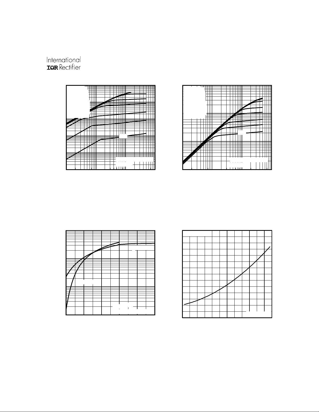
Fig 2. Typical Output CharacteristicsFig 1. Typical Output Characteristics
3.5
94A
I =
D
)
(Α
100.00
TJ = 175°C
TJ = 25°C
10.00
, Drain-to-Source Current
D
I
1.00
5.0 7.0 9.0 11.0 13.0 15.0
V
= 15V
DS
20µs PULSE WIDTH
VGS, Gate-to-Source Voltage (V)
Fig 3. Typical Transfer Characteristics
3.0
2.5
2.0
1.5
(Normalized)
1.0
0.5
DS(on)
R , Drain-to-Source On Resistance
0.0
-60 -40 -20 0 20 40 60 80 100 120 140 160 180
T , Junction Temperature
J
Fig 4. Normalized On-Resistance
V =
C
10V
GS
°
vs. Temperature
www.irf.com 3
 Loading...