

International Rectifier IRFP3206PBF Datasheet
PD - 97127
)
IRFP3206PbF
HEXFET® Power MOSFET
Applications
l High Efficiency Synchronous Rectification in SMPS
l Uninterruptible Power Supply
l High Speed Power Switching
l Hard Switched and High Frequency Circuits
Benefits
l Improved Gate, Avalanche and Dynamic dV/dt
Ruggedness
l Fully Characterized Capacitance and Avalanche
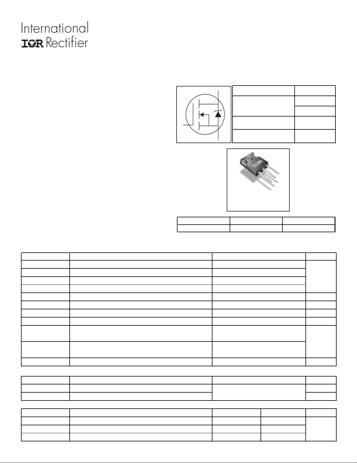
G
D
V
DSS
R
DS(on
max.
I
D
(Silicon Limited)
I
S
D
(Package Limited)
D
typ.
SOA
l Enhanced body diode dV/dt and dI/dt Capability
l Lead-Free
S
D
G
TO-247AC
GDS
Gate Drain Source
Absolute Maximum Ratings
Symbol Parameter Units
ID @ TC = 25°C Continuous Drain Current, VGS @ 10V (Silicon Limited)
@ TC = 100°C Continuous Drain Current, VGS @ 10V (Silicon Limited)
I
D
@ TC = 25°C Continuous Drain Current, VGS @ 10V (Wire Bond Limited)
I
D
I
DM
@TC = 25°C
P
D
V
GS
dv/dt
T
J
T
STG
Pulsed Drain Current
Maximum Power Dissipation
Linear Derating Factor
Gate-to-Source Voltage
Peak Diode Recovery
Operating Junction and
Storage Temperature Range
Soldering Temperature, for 10 seconds
(1.6mm from case)
Mounting torque, 6-32 or M3 screw
d
f
Max.
c
200
c
140
120
840
280
1.9
± 20
5.0
-55 to + 175
300
10lbxin (1.1Nxm)
60V
2.4m
3.0m
200A
120A
W/°C
V/ns
:
:
c
A
W
V
°C
Avalanche Characteristics
g
e
170
See Fig. 14, 15, 22a, 22b,
mJ
mJ
E
AS (Thermally limited)
I
AR
E
AR
Single Pulse Avalanche Energy
Avalanche Current
Repetitive Avalanche Energy
d
Thermal Resistance
Symbol Parameter Typ. Max. Units
R
JC
θ
R
CS
θ
R
JA
θ
Junction-to-Case
Case-to-Sink, Flat Greased Surface
Junction-to-Ambient
j –––
0.24 ––– °C/W
j ––– 40
0.54
www.irf.com 1
A
3/3/08
IRFP3206PbF
Static @ TJ = 25°C (unless otherwise specified)
Symbol Parameter Min. Typ. Max. Units
V
(BR)DSS
ΔV
(BR)DSS
R
DS(on)
V
GS(th)
I
DSS
I
GSS
R
G
Dynamic @ TJ = 25°C (unless otherwise specified)
Symbol Parameter Min. Typ. Max. Units
gfs Forward Transconductance 210 ––– ––– S
Q
g
Q
gs
Q
gd
Q
sync
t
d(on)
t
r
t
d(off)
t
f
C
iss
C
oss
C
rss
eff. (ER)
C
oss
eff. (TR)
C
oss
Drain-to-Source Breakdown Voltage 60 ––– ––– V
/ΔT
Breakdown Voltage Temp. Coefficient ––– 0.07 ––– V/°C
J
Static Drain-to-Source On-Resistance ––– 2.4 3.0
Gate Threshold Voltage 2.0 ––– 4.0 V
Drain-to-Source Leakage Current ––– ––– 20 μA
––– ––– 250
Gate-to-Source Forward Leakage ––– ––– 100 nA
Gate-to-Source Reverse Leakage ––– ––– -100
Internal Gate Resistance ––– 0.7 ––– Ω
Total Gate Charge ––– 120 170 nC
Gate-to-Source Charge ––– 29 –––
Gate-to-Drain ("Miller") Charge ––– 35
Total Gate Charge Sync. (Qg - Qgd)
––– 85 –––
Turn-On Delay Time ––– 19 ––– ns
Rise Time ––– 82 –––
Turn-Off Delay Time ––– 55 –––
Fall Time ––– 83 –––
Input Capacitance ––– 6540 ––– pF
Output Capacitance ––– 720 –––
Reverse Transfer Capacitance ––– 360 –––
Effective Output Capacitance (Energy Related)
Effective Output Capacitance (Time Related)
––– 1040 –––
––– 1230 –––
h
VGS = 0V, ID = 250μA
Reference to 25°C, I
= 10V, ID = 75A
V
mΩ
GS
= VGS, ID = 150μA
V
DS
=60V, VGS = 0V
V
DS
= 48V, VGS = 0V, TJ = 125°C
V
DS
= 20V
V
GS
= -20V
V
GS
VDS = 50V, ID = 75A
= 75A
I
D
=30V
V
DS
= 10V
= 30V
= 0V
= 50V
g
g
V
GS
I
= 75A, VDS =0V, VGS = 10V
D
V
DD
= 75A
I
D
=2.7Ω
R
G
VGS = 10V
V
GS
V
DS
ƒ = 1.0MHz, See Fig.5
= 0V, VDS = 0V to 48V i, See Fig.11
V
GS
= 0V, VDS = 0V to 48V
V
GS
Conditions
= 5mA
D
g
Conditions
d
h
Diode Characteristics
Symbol Parameter Min. Typ. Max. Units
I
S
I
SM
V
SD
t
rr
Q
rr
I
RRM
t
on
Notes:
Calculated continuous current based on maximum allowable junction
temperature. Bond wire current limit is 120A. Note that current
limitations arising from heating of the device leads may occur with
some lead mounting arrangements.
Repetitive rating; pulse width limited by max. junction
temperature.
Limited by T
RG = 25Ω, I
above this value .
Continuous Source Current ––– –––
200
c
(Body Diode)
Pulsed Source Current ––– ––– 840 A
(Body Diode)
d
Diode Forward Voltage ––– ––– 1.3 V
Reverse Recovery Time ––– 33 50 ns
––– 37 56
Reverse Recovery Charge ––– 41 62 nC
––– 53 80
Reverse Recovery Current ––– 2.1 ––– A
Forward Turn-On Time Intrinsic turn-on time is negligible (turn-on is dominated by LS+LD)
I
≤ 75A, di/dt ≤ 360A/μs, V
SD
Pulse width ≤ 400μs; duty cycle ≤ 2%.
C
eff. (TR) is a fixed capacitance that gives the same charging time
oss
, starting TJ = 25°C, L = 0.023mH
Jmax
= 120A, VGS =10V. Part not recommended for use
AS
as C
C
C
R
while V
oss
eff. (ER) is a fixed capacitance that gives the same energy as
oss
while V
oss
is measured at TJ approximately 90°C
θ
DS
is rising from 0 to 80% V
DS
A
MOSFET symbol
showing the
integral reverse
p-n junction diode.
= 25°C, IS = 75A, VGS = 0V
T
J
TJ = 25°C VR = 51V,
= 125°C IF = 75A
T
J
TJ = 25°C
= 125°C
T
J
TJ = 25°C
≤ V
DD
(BR)DSS
is rising from 0 to 80% V
DSS
Conditions
di/dt = 100A/μs
, TJ ≤ 175°C.
.
DSS
..
D
G
S
g
g
2 www.irf.com
IRFP3206PbF
1000
)
A
(
t
n
e
r
r
u
C
e
c
r
u
o
S
o
t
n
i
a
r
D
,
D
I
TOP 15V
BOTTOM 4.5V
100
VGS
10V
8.0V
6.0V
5.5V
5.0V
4.8V
4.5V
≤
60μs PULSE WIDTH
Tj = 25°C
10
0.1 1 10 100
VDS, Drain-to-Source Voltage (V)
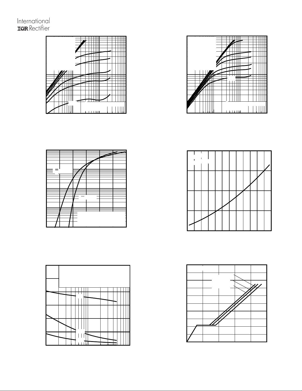
Fig 1. Typical Output Characteristics
1000
)
Α
(
t
n
100
e
r
r
u
C
e
c
r
u
o
S
o
t
n
i
a
r
D
,
D
I
TJ = 175°C
10
TJ = 25°C
1
V
= 25V
DS
≤
0.1
2.0 3.0 4.0 5.0 6.0 7.0 8.0
60μs PULSE WIDTH
VGS, Gate-to-Source Voltage (V)
)
A
(
t
n
e
r
r
u
C
e
c
r
u
o
S
o
t
n
i
a
r
D
,
I
1000
TOP 15V
BOTTOM 4.5V
100
D
VGS
10V
8.0V
6.0V
5.5V
5.0V
4.8V
4.5V
≤
60μs PULSE WIDTH
Tj = 175°C
10
0.1 1 10 100
VDS, Drain-to-Source Voltage (V)
Fig 2. Typical Output Characteristics
2.5
e
c
n
a
t
s
i
s
e
R
n
O
e
c
r
u
o
S
o
t
n
i
a
r
D
,
)
n
o
(
S
D
R
ID = 75A
V
= 10V
GS
2.0
)
d
e
z
i
l
a
1.5
m
r
o
N
(
1.0
0.5
-60 -40 -20 0 20 40 60 80 100 120 140 160 180
TJ , Junction Temperature (°C)
Fig 3. Typical Transfer Characteristics
)
F
p
(
e
c
n
a
t
i
c
a
p
a
C
,
C
12000
10000
8000
6000
4000
2000
0
1 10 100
V
= 0V, f = 1 MHZ
GS
C
= C
= C
= C
+ Cgd, C
gs
gd
+ C
ds
ds
gd
C
C
iss
rss
oss
Ciss
Coss
Crss
VDS, Drain-to-Source Voltage (V)
SHORTED
Fig 4. Normalized On-Resistance vs. Temperature
20
ID= 75A
)
V
(
16
e
g
a
t
l
o
V
e
12
c
r
u
o
S
o
t
8
e
t
a
G
,
S
4
G
V
0
0 40 80 120 160 200
VDS= 48V
VDS= 30V
VDS= 12V
Q
Total Gate Charge (nC)
G
Fig 6. Typical Gate Charge vs. Gate-to-Source VoltageFig 5. Typical Capacitance vs. Drain-to-Source Voltage
www.irf.com 3
 Loading...