

Page 1
Data Sheet No.PD60229
o
t
f
y
r
IR5001
UNIVERSAL ACTIVE ORING CONTROLLER
DESCRIPTION
The IR5001 is a universal high-speed controller and
N-channel power MOSFET driver for Active ORing and
reverse polarity protection applications. The output voltage
of the IR5001 is determined based on the polarity of the
voltage difference on its input terminals. In particular, if the
current flow through an N-channel ORing FET is from
source to drain, the output of the IR5001 will be pulled
high to Vcc, thus turning the Active ORing FET on. If the
current reverses direction and flows from drain to source
(due to a short-circuit failure of the source, for example),
the IC will quickly switch the Active ORing FET off. Typical
turn-off delay for the IR5001 is only 130nS, which helps t
minimize voltage sags on the redundant dc voltage.
Both inputs to the IC (INN and INP) as well as Vline
input contain integrated high voltage resistors and internal
clamps. This makes the IR5001 suitable for applications a
voltages up to 100V, and with a minimum number o
external components.
FEATURES
Controller / driver IC in an SO-8 package for
implementation of Active ORing / reverse polarit
protection using N-channel Power MOSFETs
Suitable for both input ORing (for carrier class
telecom equipment) as well as output ORing fo
redundant DC-DC and AC-DC power supplies
130ns Typical Turn-Off delay time
3A Peak Turn-Off gate drive current
Asymmetrical offset voltage of the internal high-speed
comparator prevents potential oscillations at light load
Ability to withstand continuous gate short conditions
Integrated voltage clamps on both comparator inputs
allow continuous application of up to 100V
Option to be powered either directly from 36-75V
universal telecom bus (100V max), or from an
external bias supply and bias resistor
Input/Output pins to determine the state of the Active
ORing circuit and power system redundancy
APPLICATIONS
-48V/-24V Input Active ORing for carrier class communication equipment
Reverse input polarity protection for DC-DC power supplies
24V/48V output active ORing for redundant AC-DC rectifiers
Low output voltage (12V, 5V, 3.3V...) active ORing for redundant DC-DC and AC-DC power supplies
Active ORing of multiple voltage regulators for redundant processor power
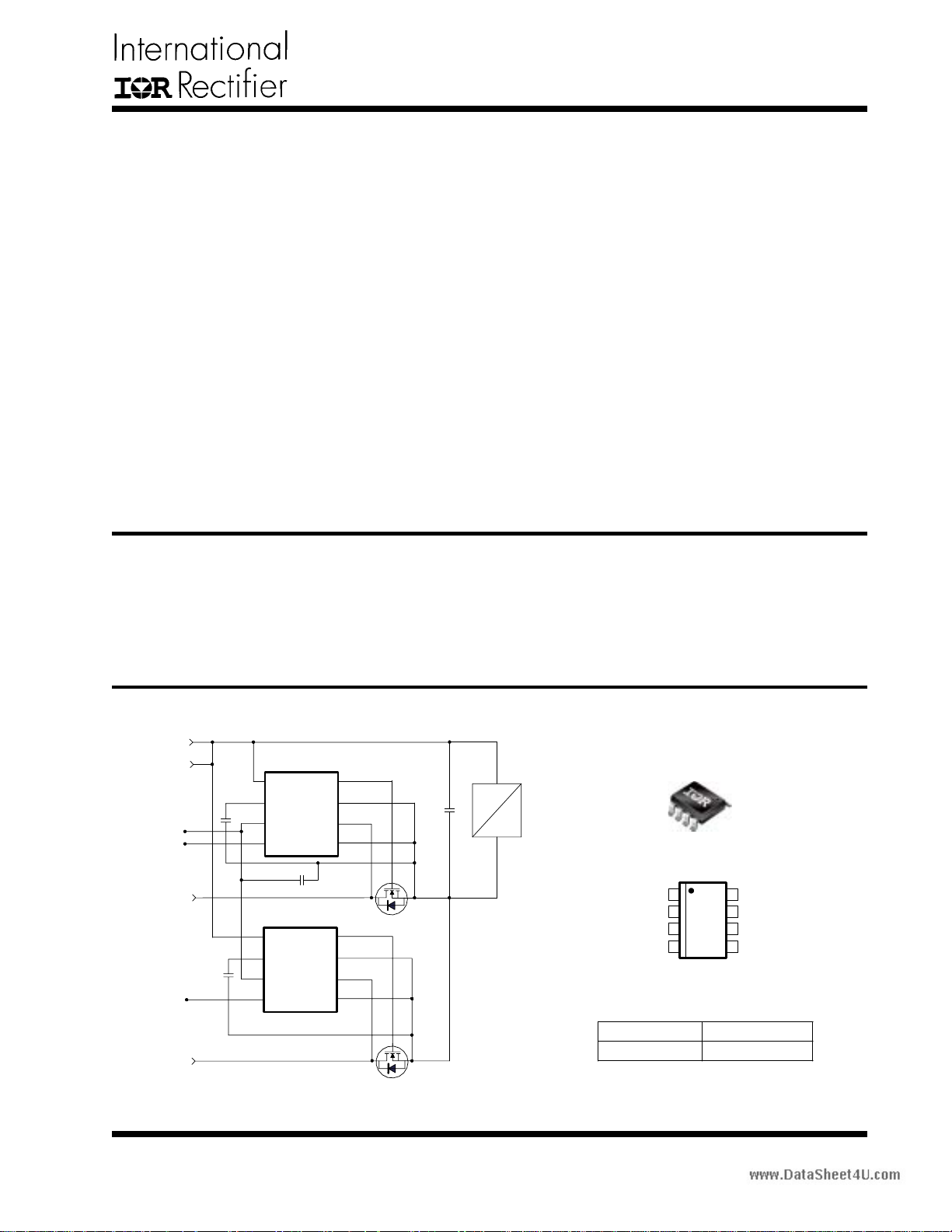
TYPICAL APPLICATION
+48V input
FET Check Puls e
-48V input A
-48V input B
A
B
FET A Status
Fet B Status
IR5001
Vline
Vcc
FETch
FETst
IR5001
Vline
Vcc
FETch
FETst
Vout
Gnd
INN
INP
Vout
Gnd
INN
INP
Figure 1 - Typical application of the IR5001 in - 48V input,
carrier class telecommunications equipment.
DC
DC
www.irf.com
PACKAGE / ORDERING
INFORMATION
Top View
Vline
1
2
Vcc
3
FETch
4
FETst
θJA=128°C/W
Ordering P/N Package
IR5001S 8 - Pin SOIC
8
Vout
7
Gnd
6
INN
5
INP
1
Page 2
IR5001
Vli
VINP=0; VINN
,
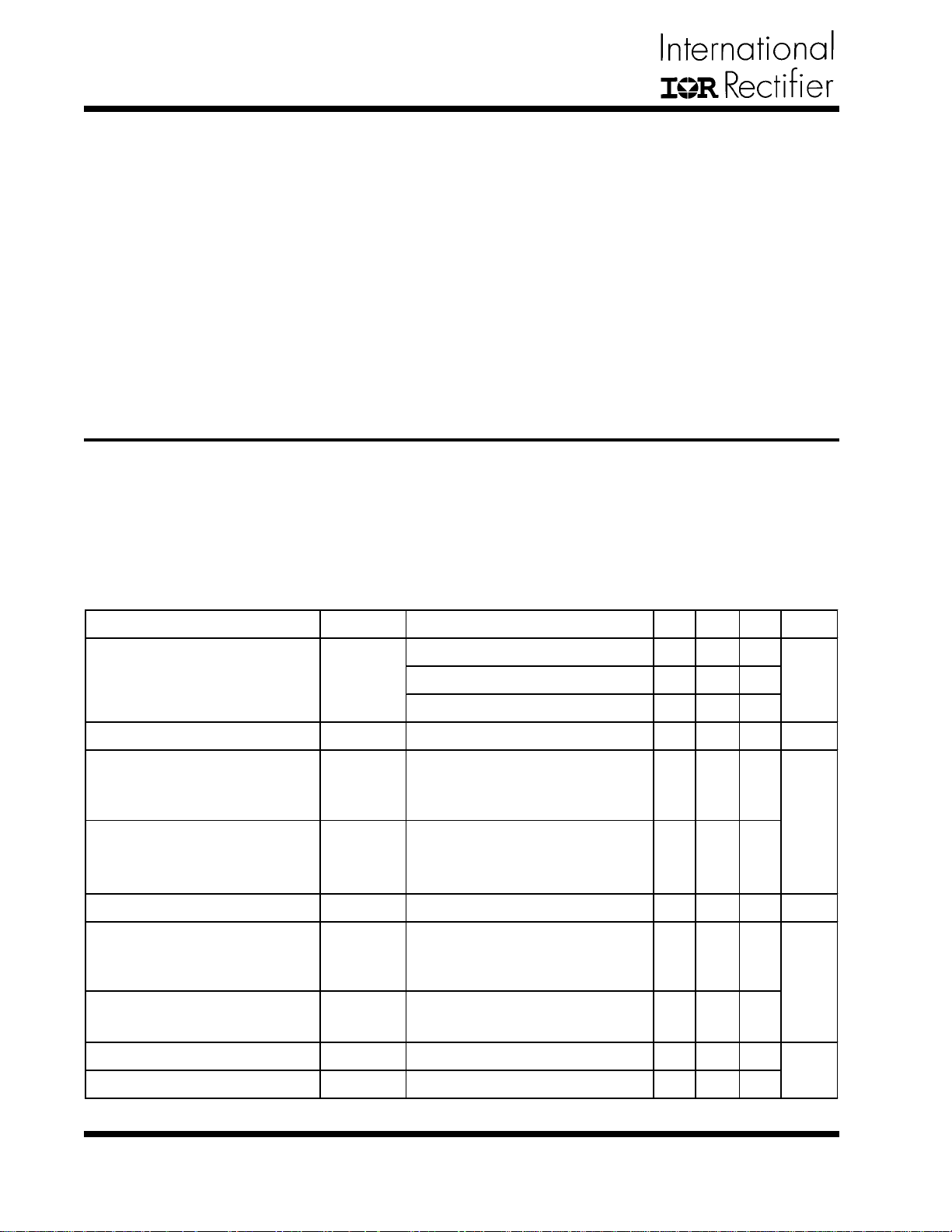
ABSOLUTE MAXIMUM RATINGS
Vline Voltage -5.0V to 100V (continuous)
Vcc Voltage -0.5V to 15VDC
Icc Current 5mA
INN, INP Voltage -5.0V to 100V (continuous)
FETch, FETst -0.5V to 5.5V
FETst Sink Current 10mA
Junction Temperature -40°C to 125°C
Storage Temperature Range -65°C to 150°C
CAUTION:
1. Stresses above those listed in "Absolute Maximum Ratings" may cause permanent damage to the device. This
is a stress only rating and operation of the device at these or any other conditions above those indicated in the
operational section of this specification is not implied.
2. This device is ESD sensitive. Use of standard ESD handling precautions is required.
.
ELECTRICAL SPECIFICATIONS
Unless otherwise specified, these specifications apply over Vline = 36V to 100V; Vcc is decoupled with 0.1uF to
Gnd, CL=10nF at Vout; INP is connected to Gnd. Typical values refer to TA=25°C. Minimum and maximum limits
apply to TA= 0°C to 85°C temperature range and are 100% production-tested at both temperature extremes. Low
duty cycle pulse testing is used which keeps junction and case temperatures equal to the ambient temperature.
PARAMETERS SYMBOL TEST CONDITION MIN TYP MAX UNITS
Vline=25V 0.14 0.3 0.5
Bias Section
Vline Bias Current
VCC output voltage Vcc(out) Vline=25V 10.2 12.5 13.9 V
UVLO Section
UVLO ON Threshold Voltage
UVLO OFF Threshold Voltage Vcc(OFF)
UVLO Hysteresis 1.6 2.3 2.8 V
Input Comparator Section
Input Offset Voltage (VINPVINN)
Input Hysteresis Voltage Vhyst
(INN) Input Bias Current I(INN) VINP=0V, VINN=36V 0.2 0.5 0.9
(INP) Input Bias Current I(INP) VINN=0V, VINP=36V 0.2 0.5 0.9
Iline
Vcc(ON)
Vos
ne=open,
Vcc increased until Vout switches
Vline=open, VINP=0, VINN=-
0.3V, Vcc is decreased until
Vout switches from HI to LO
VINP=0V and VINN Ramping up,
VOUT changes from HI to LO,
VINP=0,VINN ramping down,
Vline=36V 0.2 0.5 0.75
Vline=100V, Note 1 1.2 1.7 2.2
= -
0.3V
from LO to HI
Fig.3
Figures 3 and 4
Note 2
8.3 9.6 10.9
5.7 7.2 8.5
-7.9 -4. 0 0
13 31 44
mA
mV
mA
V
2
www.irf.com
Page 3
IR5001
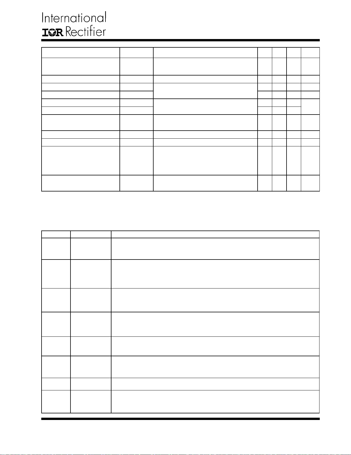
PARAMETERS SYMBOL TEST CONDITION MIN TYP MAX UNITS
Output Section
High Level Output Voltage
Low Level Output Voltage Vout LO IOL=100mA, V(INN)=+0.3V 0.1 0.1 V
Turn-On DelayTime td(on) 5 27 45 us
Rise Time tr 0.1 0.7 5 ms
Turn-Off Delay Time td(off) 110 130 170
Fall Time tf 10 26 39
FETch and FETst
FETch Sink Current
FETch Output Delay Time FETch_pd Note 1 0.8 1.8 us
FETch Threshold Vth(FETch) 0.9 1.2 1.5 V
FETst Threshold Voltage Vth(FETst)
FETst Low Level Output
Voltage
Vout HI
I(FETch) FETch=5V -0.5 -1.1 -2 uA
VOL Isink=1mA, V(INN)=-0.5V 0 50 100 mV
Vline=25V, IOH=50uA,
V(INN)=-0.3V
Vout switching from LO to HI, Fig.5
Vout switching from HI to LO, Fig.5 ns
5k resistor from FETst to 5V logic
bias.
V(INP) = Gnd, V(INN) ramping down
from 0 until FETst switches to Low.
9.5 12 14 V
-525 -300 -200 mV
Note 1: Guaranteed by design but not tested in production.
Note 2: Low Vcc output voltage corresponds to low UVLO voltage
PIN DESCRIPTIONS
PIN# PIN SYMBOL PIN DESCRIPTION
1 Vline
2Vcc
3FETch
4FETst
5INP
6INN
IC power supply pin for 36V to 75V input communications systems.
Minimum 25V has to be applied at this pin to bias the IC.
Output pin of the internal s hunt regulator, or input pin for biasing the IC via
external resistor. This pin is internally regulated at 12.5V ty pical. A
minimum 0.1uF capacitor must be connected from this pin to Gnd of IR5001.
FET check input pin. Together with FET status output pin, the FETch pin
can be used to determine the state of the Ac tive ORing circuit and power
system redundancy .
FET status output pin. Together with FETch input pin, the FETst pin c an be
used to determine the state of the Active ORing circuit and power system
redundancy.
Positive input of internal comparator. This pin should connect to the source
of N-channel Active ORing MOS FET.
Negative input pin of internal comparator. This pin should connect to the
drain of N-channel Active ORing MOSFET.
7 Gnd Ground pin of the IR5001.
8 Vout
Output pin for the IR5001. This pin is used to directly drive the gate of the
Active Oring N-Channel MOSFE T.
www.irf.com
3
Page 4
IR5001
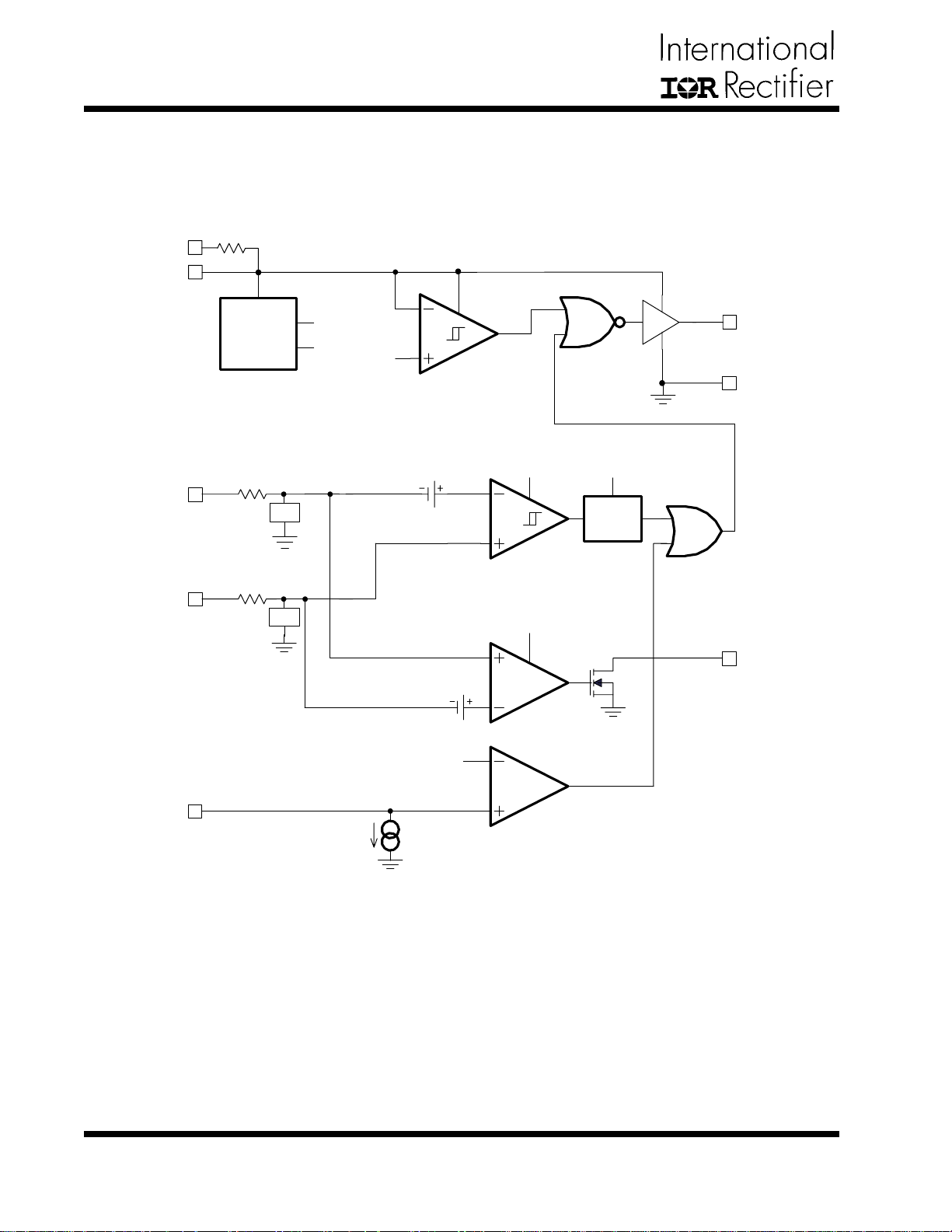
BLOCK DIAGRAM
50K
1
LINE
V
2
Vcc
INP
INN
5
6
12V Shunt
Regulator
REF
5V, V
Generator
70K
clamp
70K
clamp
8
V
5V
1.25V
9V
UVLO
3.5mV
28mV
5V
12V
Level
Shifter
OUT
7
Gnd
5V
4
FETst
0.3V
1.25V
4
FETch
3
2uA
Figure 2 - Simplified block diagram of the IR5001.
www.irf.com
Page 5

PARAMETER DEFINITION AND TIMING DIAGRAM
OUT
V
-Vos
V
INP
- V
(0,0)
HYST
V
OS
V
INN
Gnd
V
HYST
IR5001
V
OUT
V
INN
(V
=Gnd)
INP
Figure 3 - Input Comparator Offset (Vos ) and Hysteresis
Voltage (Vhyst) Definition.
10ns
90mV
50mV
0
INP
- V
INN
= 200mV
(V
INP
V
- V
V
IN
INN
)
d(on)
t
90%
50%
10%
OL
V
OUT
V
r
t
Figure 4 - Input Comparator Hysteresis Definition.
10ns
-50mV
-90mV
d(off)
t
OH
V
f
t
Figure 5 - Dynamic Parameters.
www.irf.com
5
Page 6
IR5001
)
TYPICAL OPERATING CHARACTERISTICS
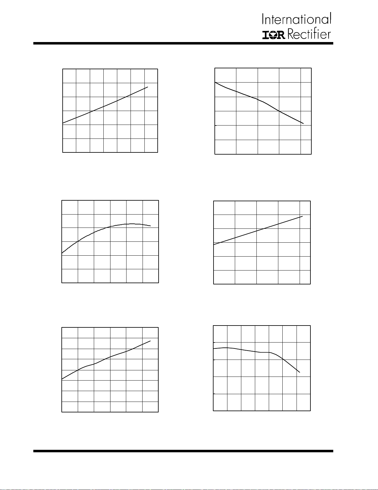
180
170
160
150
td(off) (ns)
140
130
120
-40 -20 0 20 40 60 80 100
Temperature (°C)
Figure 6 - Turn Off Delay vs. Junction Temperature
5.7
5.6
5.5
5.4
10.8
10.4
10
9.6
9.2
UVLO_upper (V)
8.8
8.4
-40 0 40 80 120
Temperature (°C)
Figure 7 - UVLO Upper Trip Point vs. Junction Temperature
28
26
24
22
5.3
Vos value (mV)
5.2
5.1
-40 -10 20 50 80 110 140
Temperature (°C)
Figure 8 - Vos vs. Junction Temperature
31
29
27
25
23
21
Hysteresis( mV)
19
17
15
-40 -10 20 50 80 110 140
Temperature (°C)
Figure 10 - INP, INN Input Hysteresis vs. Junction Temp.
Fall time (ns)
20
18
16
-40 0 40 80 120
Temperature (°C)
Figure 9 - Fall Time vs. Junction Temperature
-280
-300
-320
-340
FETst threshold (mV
-360
-380
-40-20 0 20406080100
Temperature (°C)
Figure 11 - FETst Threshold Voltage vs. Junction Temp.
6
www.irf.com
Page 7
)
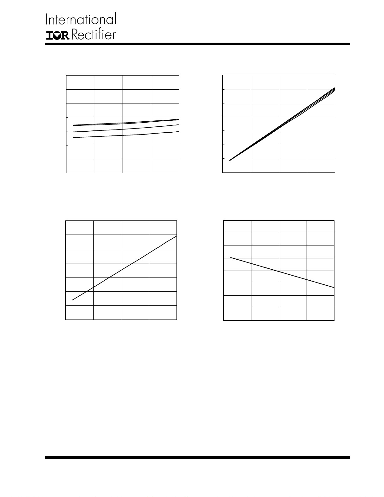
TYPICAL OPERATING CHARACTERISTICS
)
IR5001
13
12.8
12.6
12.4
Vcc (V)
12.2
12
11.8
11.6
20 40 60 80 100
Top:
Bottom:
25°C
85°C
125°C
-40°C
Vline (V)
Figure 12 - Vcc vs. Vline and Junction Temperature
1.4
1.2
1
0.8
0.6
I INN (mA
0.4
0.2
1.75
1.5
1.25
1
0.75
I Vline (mA)
0.5
0.25
0
20 40 60 80 100
Top:
Bottom:
125°C
85°C
25°C
-40°C
Vline (V)
Figure 13 - I(Vline) vs. Vline and Junction Temperature
121.0
120.5
120.0
119.5
119.0
118.5
Toff delay (nS
118.0
117.5
0
20 40 60 80 100
INN (V)
Figure 14 - Bias Current I(INN) vs. V(INN) at Vline=25V
www.irf.com
117.0
20 40 60 80 100
Vline (V)
Figure 15 - Turn Off Delay vs. Vline at Room Temperature
7
Page 8

IR5001
V
f
c
r
e
c
A
y
f
A
DETAILED PIN DESCRIPTION
line and Vcc
Vline and Vcc are the input and output pins o
the internal shunt regulator. The internal shunt
regulator regulates the Vcc voltage at ~12V. The
Vcc pin should always be by-passed with a cerami
capacitor to the Gnd pin.
Both Vline and Vcc pins can be used for biasing
the IR5001, as shown in Fig. 16. The Vline pin is
designed to bias the IR5001 directly when the
available bias voltage is above 25V and less than
100V (targeted at typical 36V – 75V telecom
applications). This connection is shown in Fig 16.a.
If the available Vbias voltage is lower than 25V, then
the IC must be biased using Vcc pin and an external
bias resistor as shown in Fig. 16.b. If the available
bias voltage is above 100V, both Vline and Vcc pins
can be used with an external bias resistor. Fo
calculation of the proper bias resistor value, see
example below.
Vbias
+
Vline
Vcc
FETch
FETst
IR5001
OUT
Gnd
INN
INP
An example of Rbias calculation is given below.
Vbias voltages used in the example are referenced
to IR5001 Gnd:
Vbias min = 12V
Vbias max = 16V
Rbias = (Vbias min – Vcc UVLOmax) / Icc min =
= (12V – 10.9V) / 0.5mA = 2.2kOhm
Next, using a minimum Vcc (10.2V), verify that Icc
with the selected Rbias will be less than 5mA:
Icc max = (Vbias max – Vcc min)/Rbias =
= (16V - 10.2V) / 2.2kOhm = 2.6mA
Since 2.6mA is below 5mA max Icc, the calculated
Rbias (2.2kOhm) can be used in this design.
INP and INN Inputs
INP and INN are the inputs of the internal highspeed comparator. Both pins have integrated onboard voltage clamps and high-voltage 70kOhm
resistors.
In a typical application, INP should be connected
to the source of the N-FET and INN to the drain. To
improve the noise immunity, the connections from
INN and INP pins to the source and drain terminals
of the N-FET should be as short as possible.
The (INP – INN) voltage difference determines
the state of the Vout pin of the IR5001. When the
body diode of the Active ORing N-FET is forwardbiased and the current first starts flowing, the
voltage difference INP – INN will quickly rise toward
~700mV (typical body diode forward voltage drop).
s soon as this voltage exceeds Vhyst – Vos
(27mV typical), the Vout of the IR5001 will be pulled
high, turning the channel of the active ORing FET
on. As the channel of the N-FET becomes full
enhanced, the (INP – INN) will reduce and stabilize
Vbias
+
Rbias
Vline
Vcc
FETch
FETst
a)
IR5001
OUT
Gnd
INN
INP
at the value determined by the source-drain current,
Figue 16 - Biasing options for IR5001
b)
When the Vcc pin is used for biasing th
IR5001, the Vbias must always be higher than the
maximum value of the Vcc UVLO threshold (10.9V).
The Rbias resistor should always be connected
between the Vbias voltage source and Vcc pin. The
Rbias resistor is selected to provide adequate Ic
current for the IC. The minimum required Icc to
guarantee proper IC operation under all conditions is
0.5mA. The maximum Icc is specified at 5mA.
Isd, and Rds(on) of the N-FET:
(INP – INN) steady state = Isd * R
DS(on).
If for some reason (due to a short-circuit failure o
the source, for example), the current reverses
direction
and tries to flow from drain to source, the
(INP – INN) will become negative; The IR5001 will
then quickly pull its output low, switching the ORing
FET off. For considerations regarding the selection
of the Active ORing N-FET and R
DS(on)
, see
pplications Information Section.
The offset voltage of the internal high-speed
comparator is centered around negative 4mV, and is
always less than 0mV. This asymmetrical offset
8
www.irf.com
Page 9

IR5001
V
y
w
t
t
e
t
f
guarantees that once the ORing N-FET is
conducting and Vout of the IR5001 is high (FET
current flows from source to drain), the current must
reverse the direction before the IR5001 will switch
the FET off. The asymmetrical offset voltage
prevents potential oscillations at light load that could
otherwise occur if the offset voltage was centered
around 0mV (as is the case in standard
comparators).
out
Vout is the output pin of the IR5001, and connects
directly to the gate of the external Active ORing NFET. The voltage level at the Vout pin is typically a
diode drop lower than the Vcc voltage.
FETst and FETch
FETch and FETst pins are diagnostic pins that can
be used to determine the status of the Active ORing
circuit.
is an open-drain output pin. When the voltage
FETst
difference between VINP - VINN is less than 0.3V,
the FETst pin will be logic high. This is normally the
case when Active ORing is operating properly (VINP
- VINN is less than ~100mV). If the Active ORing
FET is not turned on while the IR5001 is properl
biased, the output of the FETst pin will be logic lo
(only the body diode of the N-FET is conducting, and
VINP - VINN is ~700mV).
FETch
it is not possible to determine if the diode is
pin. In traditional systems with diode ORing,
functioning properly unless external circuitry is used.
For example, the diode could be failed short, and the
system would not be aware of it until the source fails
and the whole system gets powered down due to
lost redundancy (shorted diode failed to isolate the
source failure). With the FETch pin it is possible to
perform a periodic check of the status of the Active
ORing circuit to assure that system redundancy is
maintained.
In the IR5001, the FETch pin is an input pin tha
can be used to turn off the output of the IR5001:
logic high signal on FETch will pull the Vout pin low,
and turn-off the channel of the Active ORing N-FET.
This will force the current to flow through the body
diode, resulting in VINP – VINN voltage increase
from less than ~100mV, to ~700mV. This voltage
increase will be reported at FETst pin, which will
switch from logic high to logic low, and indicate tha
the Active ORing circuit is working properly. Failur
of the FETst pin output to change from logic high to
logic low would indicate that the Active ORing circui
may not be operating as designed, and the system
may no longer have power redundancy. For details
on how to use this feature consult IR5001 Evaluation
Kit,
P/N IRDC5001-LS48V
If t the FETch pin is not used, it should be tied to
ground (for noise immunity purposes). If not used,
FETst pin should be left open.
Gnd
In typical target applications, the ground pin (Gnd) o
IR5001 is connected to the source of the Active
ORing N-FET.
.
www.irf.com
9
Page 10

IR5001
f
APPLICATION INFORMATION
The IR5001 is designed for multiple active ORing
and reverse polarity protection applications with
minimal number of external components. Examples
of typical circuit connections are shown below.
Negative Rail ORing/Reverse Polarity Protection
A typical connection of the IR5001 in negative
rail Active ORing or reverse polarity protection is
shown in Fig. 17. In this example, IR5001 is biased
directly from the positive rail. However, any of the
biasing schemes shown in Fig. 16 can be used.
For input ORing in carrier-class communications
boards, one IR5001 is used per feed. This is shown
in Fig.1. An evaluation kit is available for typical
system boards, with input voltages of negative 36V
to negative 75V, and for power levels from 30W to
about 300W. The p/n for the evaluation kit is
IRDC5001-LS48V. This evaluation kit contains
detailed design considerations and in-circuit
performance data for the IR5001.
Vin +
IR5001
Vline
Rbias
+
Vbias
Vin -
Figure. 17 Connection of INN, INP, and Gnd for negative
rail Active ORing or reverse polarity protection.
Vout +
Rbias
+
Vbias
Vout -
Figure. 18. Connection of INN,INP, and Gnd when the
MOSFET is placed in the path of positive rail.
Vcc
FETch
FETst
Vline
Vcc
FETch
FETst
IR5001
OUT
Gnd
OUT
INN
INP
Gnd
INN
Load
Redundant Vi n -
Redundant Vout +
Load
INP
Positive Rail ORing / Ground ORing in
Communications Boards
An example of a typical connection in positive
rail ORing is shown in Fig. 18. Typical applications
are inside redundant AC-DC and DC-DC power
supplies, or on-board ORing. For positive rail ORing,
an additional Vbias voltage above the positive rail is
needed to bias the IR5001.
An evaluation kit for high-current 12V positive
rail ORing is available under p/n IRAC5001-
HS100A, demonstrating performance of the IR5001
at 100A output current.
Considerations for the Selection of the Active
ORing N-Channel MOSFET
Active ORing FET losses are all conduction
losses, and depend on the source-drain current and
DS(on)
R
virtually eliminated if a FET with very low R
was used. However, using arbitrarily low R
of the FET. The conduction loss could be
DS(on)
is
DS(on)
not desirable for three reasons:
1. Turn off propagation delay. Higher R
DS(on)
will
provide more voltage information to the internal
comparator faster, and will result in faster FET
turn off protection in case of short-circuit of the
source (less voltage disturbance on the
redundant bus.
2. Undetected reverse (drain to source) current
flow. With the asymmetrical offset voltage, some
small current can flow from the drain to source
of the ORing FET and be undetected by the
IR5001. The amount of undetected drain-source
current depends on the R
MOSFET and its R
DS(on)
of the selected
DS(on)
. To keep the reverse
(drain-source) current below 5 – 10% of the
nominal source-drain state, the R
DS(on)
of the
selected FET should produce 50mV to 100mV o
the voltage drop during nominal operation.
3. Cost. With properly selected R
DS(on)
, Active
ORing using IR5001 can be very cost
competitive with traditional ORing while
providing huge power loss reduction. For
example, a FET with 20mOhm R
DS(on)
results in
60mV voltage drop at 3A; associated power
savings compared to the traditional diode ORing
(assuming typical 0.6V forward voltage drop) is
ten fold(0.18W vs. 1.8W)! Now assume that
FET R
was 10mOhm. The power loss
DS(on)
would be reduced by additional 90mW, which is
negligible compared to the power loss reduction
already achieved with 20mOhm FET. But to get
this negligible saving, the cost of the Active
ORing FET would increase significantly.
10
www.irf.com
Page 11

IR5001
j
r
In a well - designed Active ORing circuit, the
Rds(on) of the Active ORing FET should generate
between 50mV to 100mV of (INP – INN) voltage
during normal, steady state operation. (The normal
operation refers to current flowing from the source to
drain of the Active ORing FET, half of the full-load
system current flowing through each OR-ed source,
at nominal input voltage). Maximum power
dissipation under worst-case conditions for the FET
should be calculated and verified against the data
sheet limits of the selected device.
IR5001 Thermal considerations
Maximum junction temperature of the IR5001 in an
application should not exceed the maximum
operating junction temperature, specified at 125°C:
Tj = Pdiss * Rtheta j-a + Tamb <= Tj (max),
where Rtheta j-a is the thermal resistance from
unction to ambient thermal resistance (specified at
128 °C/W), Pdiss is IC power dissipation, and Tamb
is operating ambient temperature.
The maximum power dissipation can be estimated
as follows:
Pdiss < (Tj max – Tamb max) / Rtheta j-a
Since Tj max= 125 °C, Tamb = 85 °C, and Rtheta j-a
= 128 °C/W, the maximum power dissipation allowed
is:
Pdiss max = (125 – 85) / 128 = 0.3W
With proper selection of Icc (as discussed in the
Detailed Pin Description), the maximum powe
dissipation will never be exceeded (Max Icc * Max
Vcc = 10mA * 13.9V = 0.14W).
Layout Considerations
INN and INP should be connected very close to
the drain and source terminal of the Active ORing
FET. PCB trace between the Vout pin and the gate
of the N-FET should also be minimized. A minimum
of 0.1uF decoupling capacitor must be connected
from Vcc to Gnd of the IR5001and should be placed
as close to the IR5001 as possible. Ground should
be connected to the source of N-FET separately
from the INP pin.
www.irf.com
11
Page 12

IR5001
(S) SOIC Package
8-Pin Surface Mount, Narrow Body
H
A
B C
E
PIN NO. 1
DETAIL-A
L
D
0.38 +/- 0.015 x 45°
T
F
G
SYMBOL
A
B
C
D
E
F
G
H
J
K
L
T
K
J
8-PIN
1.27 BSC
0.53 REF
7° BSC
0°
MAX
4.98
0.46
3.99
1.72
0.25
0.25
6.20
8°
1.27
1.57
MIN
4.80
0.36
3.81
1.52
0.10
I
0.19
5.80
0.41
1.37
DETAIL-A
I
12
NOTE: ALL MEASUREMENTS ARE IN MILLIMETERS.
www.irf.com
Page 13

PACKAGE SHIPMENT METHOD
IR5001
PKG
DESIG
S
PACKAGE
DESCRIPTION
SOIC, Narrow Body
PIN
COUNT
8
1 11
Feed Direction
Figure A
PARTS
PER TUBE
95
PARTS
PER REEL
2500
T & R
Orientation
Fig A
This product has been designed and qualified for the industrial market
IR WORLD HEADQUARTERS: 233 Kansas St., El Segundo, California 90245, USA Tel: (310) 252-7105
TAC Fax: (310) 252-7903
Visit us at www.irf.com for sales contact information
Data and specifications subject to change without notice. 4/8/2005
www.irf.com
13
 Loading...