


IR3721
DATA SHEET
Power Monitor IC with
Analog Output
FEATURES
Accurate TruePower
• 2.5% static accuracy
• Minimizes dynamic errors
Minimizes power dissipation
• 5mV - 150mV full scale current range
Versatile
• Monitors power or current
• Single buck or multiphase converters
• Inductor DCR or resistive shunt sensing
Simple add-on to existing converters
10 pin 3x3 DFN lead free package
RoHS compliant
TM
monitor
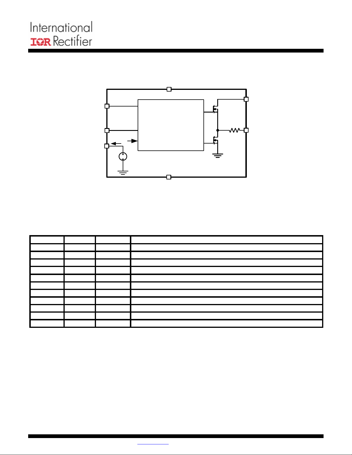
TYPICAL APPLICATION CIRCUIT
DESCRIPTION
The IR3721 is a versatile power or current monitor IC
for low-voltage DC-DC converters. The IR3721
monitors the inductor current in buck or multiphase
converters using either a current sensing resistor or the
inductor’s winding resistance (DCR). The output (DI) is
a pulse code modulated signal whose duty ratio is
proportional to the inductor current. An analog voltage
that is proportional to power is realized by connecting
V
to VO and connecting an RC filter to DI.
K
The IR3721 uses Patent Pending TruePower
technology to accurately capture highly dynamic power
waveforms typical of microprocessor loads.
TM
ORDERING INFORMATION
Device Package Order Quantity
IR3721MTRPBF 10 lead DFN (3x3 mm body) 3000 piece reel
IR3721MPBF 10 lead DFN (3x3 mm body) Sample Quantity
Page 1 of 16 www.irf.com 01/04/08

ABSOLUTE MAXIMUM RATINGS
IR3721
DATA SHEET
Absolute Maximum Ratings (Referenced to GND)
VDD:.................................................................3.9V
All other Analog and Digital pins......................3.9V
Operating Junction Temperature .... -10°C to 150°C
Storage Temperature Range .......... -65°C to 150°C
ESD Rating ............HBM Class 2 JEDEC Standard
MSL Rating ..................................................Level 2
Reflow Temperature ..................................... 260°C
Stresses beyond those listed under “Absolute Maximum Ratings” may cause permanent damage to the device.
These are stress ratings only and functional operation of the device at these or any other conditions beyond those
indicated in the operational sections of the specifications are not implied. Exposure to absolute maximum rating
conditions for extended periods may affect device reliability.
ELECTRICAL SPECIFICATIONS
Unless otherwise specified, these specifications apply: VDD = 3.3V ± 5%, 0oC ≤ TJ ≤ 125oC, 0.5 ≤ Vo ≤ 1.8 V, and
operation in the typical application circuit. See notes following table.
PARAMETER TEST CONDITION MIN TYP MAX UNIT
BIAS SUPPLY
VDD Turn-on Threshold, VDDUP 3.10 V
VDD Turn-off Threshold, VDDDN 2.4 V
VDD UVLO Hysteresis DI output low when off 75 mV
VDD Operating Current, ICC 350 450 μA
VOLTAGE REFERENCE
VRT Voltage RT = 25.5k Ω 1.452 1.493 1.535 V
RT resistance range Note 1 25.5
ΔΣ CONVERTER
Vo common mode range 0.5 1.8 V
Duty Ratio Accuracy V
Duty Ratio Accuracy V
=20 mV, VO=1V,
DCR
R
=25.5kΩ, R
T
T
=65°C, Note 1
j
=20 mV, VO=1V,
DCR
=25.5kΩ, R
R
T
CS1+RCS2
CS1+RCS2
2.5 %
=600 Ω
4 %
=600 Ω,
Note 1
Sampling frequency, f
435 512 589 kHz
CLK
Comparator Offset -0.5 +0.5 mV
CS pin input current, ICS DI output low -250 +250 nA
DIGITAL OUTPUT
VK pin voltage range 0.5 1.8 V
DI source resistance 1250 2000 3000
NOTES:
1. Guaranteed by design
kΩ
Ω
Page 2 of 16 www.irf.com 01/04/08
BLOCK DIAGRAM
IR3721
DATA SHEET
VDD
VK
VO
VCS
V
RT
I
REF
I
REF
VO
TruePower™
VCS
result out
DI
result out/
IR3721
GND
IC PIN DESCRIPTION
NAME NUMBER I/O LEVEL DESCRIPTION
VCS 1 Analog Current sensing input, connect through resistor to sensing node
VO 2 Analog Current sensing reference connect to output voltage
VRT 3 Analog RT thermistor network from this pin to GND programs thermal monitor
GND 4
VDD 5 3.3V IC bias supply
GND 6 Connect to pin 4
GND 7 Connect to pin 4
DI 8 Analog Power Monitor output; connect to output filter
VK 9 1.8V Connect to fixed voltage or VO, multiplied by DI to become analog output
VDD 10 3.3V Connect to pin 5
BASE PAD Connect to pin 4
Bias return and signal reference
Page 3 of 16 www.irf.com 01/04/08

IC PIN FUNCTIONS
VDD PINS
IR3721
DATA SHEET
VRT PIN
These pins provide operational bias current to circuits
internal to the IR3721. Bypass them with a high
quality ceramic capacitor to the GND pins.
GND PINS
These pins return operational bias current to system
ground. VO is measured with respect to GND. The
GND pin sinks reference current established by the
external resistor R
.
T
VO PIN
Since this pin measures DCR voltage drop it is critical
that it be Kelvin connected to the buck inductor
output. Power accuracy may be degraded if the
voltage at this pin is below VO
min
.
VCS PIN
A switched current source internal to the IR3721
maintains the average voltage of this pin equal to the
voltage of the VO pin. The average current into this
pin is therefore proportional to buck inductor current.
A voltage reference internal to the IR3721 drives the
V
pin while the pin current is monitored and used to
RT
set the amplitude of the current monitor switched
current source I
a precision resistor network R
. Connect this pin to GND through
REF
. This network may
T
include provision for canceling the positive
temperature coefficient of the buck inductor’s DC
resistance (DCR).
VK PIN
The voltage of the VK pin is used to modulate the
amplitude of the DI pin. This is one of the terms used
to determine the product of the multiplier output. If VK
is connected to a fixed voltage then the output of the
multiplier is proportional to current. If VK is connected
to the buck converter output voltage then the output
of the DI driven RC filter is proportional to power.
DI PIN
The Dl pin output has a duty ratio proportional to the
current into VCS, and an amplitude equal to the
voltage at the VK pin. The DI pin is intended to drive
an external low pass filter. The output of this filter is
the product of the current and voltage terms.
Page 4 of 16 www.irf.com 01/04/08

FUNCTIONAL DESCRIPTION
Please refer to the Functional Description Diagram
below. Power flow from the buck converter inductor is
the product of output voltage times the current I
L
flowing through the inductor.
Power is measured with the aid of International
Rectifier’s proprietary TruePower™ circuit. Current is
converted to a duty ratio that appears at the DI pin.
The duty ratio of the DI pin is
DI
RATIODUTY
RR
⋅
DCRI
L
=
R
T
⋅
)+(
2CS1CS
V
Τ
R
Equation 1
The full-scale current that can be measured
corresponds to a duty ratio of one.
I
L
Vin
R
L
CS1
DCR
C
CS1
C
CS2
VCS
R
CS2
VO
The amplitude of the DI pin is the voltage appearing
at pin VK. If a fixed voltage is applied to VK then the
output of the RC filter driven by DI will be proportional
to inductor current I
.
L
If VO is applied to V
as shown in the figure then the
K
output of the DI driven RC network will be
proportional to power. The full-scale voltage that can
be measured is established on the chip to be 1.8V.
The full scale power P
that can be measured is the
FS
product of full-scale voltage and full scale current.
Vo
VDD
VK
IR3721
DI
Power
V
RT
R
T
GND
Figure 1 Functional Description Diagram
Page 5 of 16 www.irf.com 01/04/08
THERMAL COMPENSATION FOR INDUCTOR DCR CURRENT
SENSING
The positive temperature coefficient of the inductor
DCR can be compensated if R
varies inversely
T
proportional to the DCR. DCR of a copper coil, as a
function of temperature, is approximated by
TCRTTTDCRTDCR -1
)⋅)(+(⋅)(=)(
CuRR
Equation 2
T
is some reference temperature, usually 25 °C, and
R
TCR
is the resistive temperature coefficient of
Cu
copper, usually assumed to be 0.39 %/°C near room
temperature. Note that equation 2 is linearly
increasing with temperature and has an offset of
DCR(T
If R
) at the reference temperature.
R
incorporates a negative temperature coefficient
T
thermistor then temperature effects of DCR can be
minimized. Consider a circuit of two resistors and a
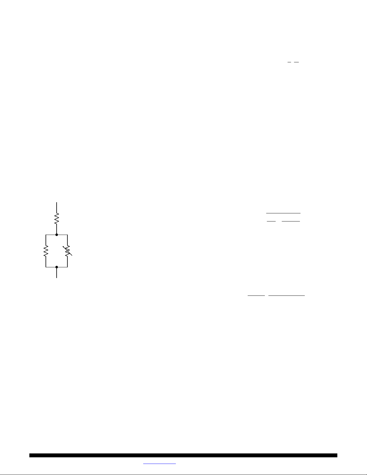
thermistor as shown below.
Rs
⎛
⎜
β
⎜
⎝
⋅)(=)(
eTRTR
0
thth
⎞
⎞
⎛
11
⎟
⎟
⎜
-
⎟
⎜
⎟
TT
0
⎠
⎝
⎠
Equation 3
where R
temperature T, R
the reference temperature T
(T) is the thermistor resistance at some
th
) is the thermistor resistance at
th(T0
, and β is the material
0
constant provided by the thermistor manufacturer.
Kelvin degrees are used in the exponential term of
equation 3. If R
is large and RP is small, the
S
curvature of the equivalent network resistance can be
reduced from the curvature of the thermistor alone.
Although the exponential equation 3 can never
compensate linear equation 2 at all temperatures, a
spreadsheet can be constructed to minimize error
over the temperature interval of interest. The
equivalent resistance R
of the network shown as a
T
function of temperature is
+=)(
RTR
sT
1
+
11
)(
TRR
thp
RthRp
Figure 2 R
If Rth is an NTC thermistor then the value of the
network will decrease as temperature increases.
Unfortunately, most thermistors exhibit far more
variation with temperature than copper wire. One
equation used to model thermistors is
Network
T
Equation 4
using R
(T) from equation 3.
th
Equation 2 may be rewritten as a new function of
temperature using equations 2 and 4 as follows:
()
+
FS
V
Τ
R
=)(
TI
⋅
)(
TR
T
RR
2CS1CS
)(
TDCR
Equation 5
With Rs and Rp as additional free variables, use a
spreadsheet to solve equation 5 for the desired full
scale current while minimizing the I
(T) variation
FS
over temperature.
Page 6 of 16 www.irf.com 01/04/08

TYPICAL 2-PHASE DCR SENSING APPLICATION
The IR3721 is capable of monitoring power in a
multiphase converter. A Two Phase DCR Sensing
Circuit is shown below. The voltage output of any
phase is equal to that of any and every other phase
because they are electrically connected and
monitored at VO as before.
Output current is the sum of the two inductor currents
(I
+ IL2). Superposition is used to derive the transfer
L1
function for multiphase sensing. The voltage on R
due to I
L1
is
)||(
RR
32
⋅⋅
DCRI
L
11
CSCS
)||(+
RRR
321
CSCSCS
CS2
Likewise, the voltage on RCS2 due to IL2 is
)||(
RR
12
⋅⋅
DCRI
L
22
CSCS
)||(+
RRR
123
CSCSCS
The current through R
currents is I
. From the two equations above
CS
I
=
CS
due to both inductor
CS2
+
++
RDCRIRDCRI
122311
CSLCSL
RRRRRR
323121
CSCSCSCSCSCS
The duty ratio of DI is
RI
⋅
DI
DUTYRATIO
=
TCS
V
REF
If DCR1=DCR2, and RCS1=RCS3, then I
can be
CS
simplified to
I
=
CS
DCRII
⋅)+(
LL
2
+
121
RR
21
CSCS
and the DI duty ratio simplifies to
⋅⋅)+(
RDCRII
T2L1L
DI
DUTYRATIO
=
⋅)+(
VR2R
Τ
R2CS1CS
Full scale current occurs when DI duty ratio becomes
one.
Figure 3 Two Phase DCR Sensing Circuit
Page 7 of 16 www.irf.com 01/04/08

RESISTOR SENSING APPLICATION
The Resistor Sensing Circuit shown below is an
example of resistive current sensing. Because the
voltage on the shunt resistor is directly proportional to
the current I
not need to match the L / DCR time constant.
through the inductor, R
L
Phase 1
CS2
and C
I
L
CS2
DCR
do
L
Buck
Converter
R
Power
Return
CS2
VDD
VDD
VDD
Bypass
V
Cap
RT
SHUNT
C
VCS
IR3721
Because the value of the shunt resistance does not
change with temperature as the inductor DCR does,
can be a fixed resistor.
R
T
VO
CS2
VO
VK
DI
Power
R
T
GND
Figure 4 Resistor Sensing Circuit
Page 8 of 16 www.irf.com 01/04/08

COMPONENT SELECTION GUIDELINES
Use a 0.1 μF, 6.3V, X7R ceramic bypass capacitor
from VDD to GND and from VK to GND.
Filter the DI output with an RC filter to give a stable
analog representation of the current or power. Some
of the DI source resistance of this filter is internal to
the IR3721 and specified in the electrical
specifications table. Add twenty thousand to fifty
thousand additional ohms externally to minimize
resistance variation. As the DI source resistance
increases beyond these guidelines, the voltage
measurement error caused by non-ideal voltmeter
conductance will increase.
Select a filter capacitor that limits 512 kHz sampling
frequency ripple to an acceptable value. Sampling
frequency ripple will appear as an error, but can be
reduced 20 dB for each decade that the filter corner
frequency is below 512 kHz. Select a capacitor value
that achieves the desired balance between low
sampling frequency ripple and adequate bandwidth.
Resistor current sensing
For resistor current sensing select a precision resistor
for R
inside the RT resistance range limits specified
T
in the Electrical Specifications table, such as 25.5kΩ
and 1% tolerance.
Next, select a shunt resistor that will provide the most
current sensing voltage while also considering the
allowable power dissipation limitations. The DI output
will saturate to the VK voltage when full scale current
I
flows through this shunt. Recommended
FS
maximum current sensing voltage range is 5 to 150
mV. Maximum sensing voltages less than 5 mV will
cause comparator input offset voltage errors to
dominate, and voltages larger than 150 mV will cause
comparator leakage current, I
Select R
resistor from (R
to be the next higher standard value
CS2
SHUNT·IFS·RT
accommodate full scale current I
Bypass VCS to VO with capacitor C
, errors to dominate.
CS
) / VRT in order to
.
FS
. The value of
CS2
this capacitor limits the bandwidth, but is required
because it is the integrator of the delta sigma
modulator. Consider selecting the value of C
CS2
to
place a filter corner frequency at 5 kHz, which will
reduce sampling ripple by 40 dB.
DCR current sensing
Select an R
45.3kΩ. Consider the R
network resistance between 20kΩ and
T
network of Figure 5 for DCR
T
current sensing.
15.0 kΩ, 1%
Figure 5 R
The resistance of the network above at 25°C, R
is 37.58kΩ. Over temperature R
copper resistance, DCR(25)·(1+(T-25)·0.0039),
divided by (DCR(25)·( R
results, and plotted as nominal error in Figure 6.
5%
4%
3%
2%
1%
0%
-1%
Nominal error
-2%
-3%
-4%
-5%
Figure 6 Nominal error vs. Temperature
Note that the error due to temperature compensation
at 25°C is zero, assuming ideal R
other temperatures the results are over or under
reported by the factor in percent indicated.
Proceed to calculate R
R
plus R
CS1
Again, I
voltage establishing the current in R
Estimate the capacitance C
equation.
26.1 kΩ, 1%
2.00 kΩ, 1%
Murata Thermistor
NCP15WB473F03RC
47 kΩ, 1%
network
T
(25),
(T) is multiplied by
T
(25)) to normalize the
T
020406080100
Temperature [°C]
T
components. At
T
, defined as the sum of
, as follows.
CS2
R
SUM=IFS
SUM
·DCR(25) ·RT(25) / VRT
is full scale current and VRT is the reference
FS
.
T
with the following
CS1
L
⋅
C
>
CS
1
4
25
RDCR
⋅)(
SUM
Page 9 of 16 www.irf.com 01/04/08

Choose a standard capacitor value larger than
indicated by the right hand side of the inequality
above.
Calculate the equivalent resistance R
.
eq
= L / (DCR(25) ·C
R
eq
CS1
)
We now have two equations, R
Req = (R
and R
· R
CS2
) / (R
CS1
using the following two equations.
CS2
CS1
+ R
= R
SUM
CS2
CS1
). Calculate R
+ R
CS2
CS1
and
⎛
⎜
⎜
RR
⎜
⋅=
SUMCS1
⎜
⎜
⎜
⎝
411
⋅+
-
2
⎞
R
eq
⎟
⎟
R
SUM
⎟
and
⎟
⎟
⎟
⎠
⎛
⎜
--
411
⎜
RR
⎜
⋅=
SUM2CS
⎜
⎜
⎜
⎝
⋅
2
⎞
R
eq
⎟
⎟
R
SUM
⎟
⎟
⎟
⎟
⎠
Use the next higher standard 1% value than indicated
in the equations above. This will insure that full scale
current can be measured.
Bypass VCS to VO with capacitor C
. The value of
CS2
this capacitor limits the bandwidth, but is required
because it is the integrator of the delta sigma
modulator. Consider selecting the value of C
CS2
to
place a filter corner frequency at 5 kHz, which will
reduce sampling ripple by 40 dB.
Page 10 of 16 www.irf.com 01/04/08

LAYOUT GUIDELINES
Refer to figures 7 through 11 for guidance laying out
the IR3721. These guidelines also apply to resistive
current sensing. The following guidelines will
minimize sources of noise and error, which is
required because millivolt level signals correspond to
amps of inductor current.
1. Place the capacitor Ccs2 close to the VO and
VCS pins of the IR3721. Treat VO and VCS as a
differential signal pair back to the IC as shown in
the elliptical area designated #1 of figure 8.
2. Sense the inductor (or shunt) Kelvin style at its
terminals. Route the leads back as a differential
pair. Refer to area #2 of figure 8.
3. Route signal VOUT back to the IC VK pin on its
own dedicated trace. Refer to area #3 of figure 8.
4. Place the thermistor near the inductor. Refer to
area #4 of figure 8. Route the thermistor leads
back to the rest of the network using differential
traces. Mount the rest of the thermistor network
consisting of Rs, Rp, and R1 close to the IC.
L1
1 2
Rcs 1
Ccs 1
Rcs 2
Ccs 2
Rs
U1
1
CS
2
VO
3
RT
4
GND_1
VCC5GND_ 4
VCC_ 1
GND_ 3
IR3721
5. Use an isolated dedicated ground plane
connected only to components associated with
the IR3721 that connect to GND as shown in
figure 9. Connect this dedicated ground plane at
one location only to the ground of the monitored
voltage. The thermally relived via in figure eight
illustrates this connection.
6. Bypass IC VDD pin 5 to GND pin 4 with a high
quality 0.1 μF ceramic capacitor. Refer to area #6
of figure 8.
7. Bypass the IC VK pin to GND with a high quality
0.1 μF ceramic capacitor. Refer to area #7 of
figure 8.
VOUT
VOUT
10
9
VK
8
DI
7
6
R_DI_FILT
DI_FILT
VDD
Figure 7 Example schematic
C_VDD
Rth
Rp
0
1 2
R1
0.1uF
C_VK
0.1uF
C_DI_FILT
GND
Page 11 of 16 www.irf.com 01/04/08

2
3
4
1
6
Figure 8 Layer 1
7
Figure 10 Layer 3
Figure 9 Layer 2
Figure 11 Layer 4
Page 12 of 16 www.irf.com 01/04/08

PCB PAD AND COMPONENT PLACEMENT
Figure 12 below shows suggested pad and component placement.
Figure 12 Pad placement
Page 13 of 16 www.irf.com 01/04/08

SOLDER RESIST
Figure 13 below shows suggested solder resist placement.
Figure 13 Solder resist
Page 14 of 16 www.irf.com 01/04/08
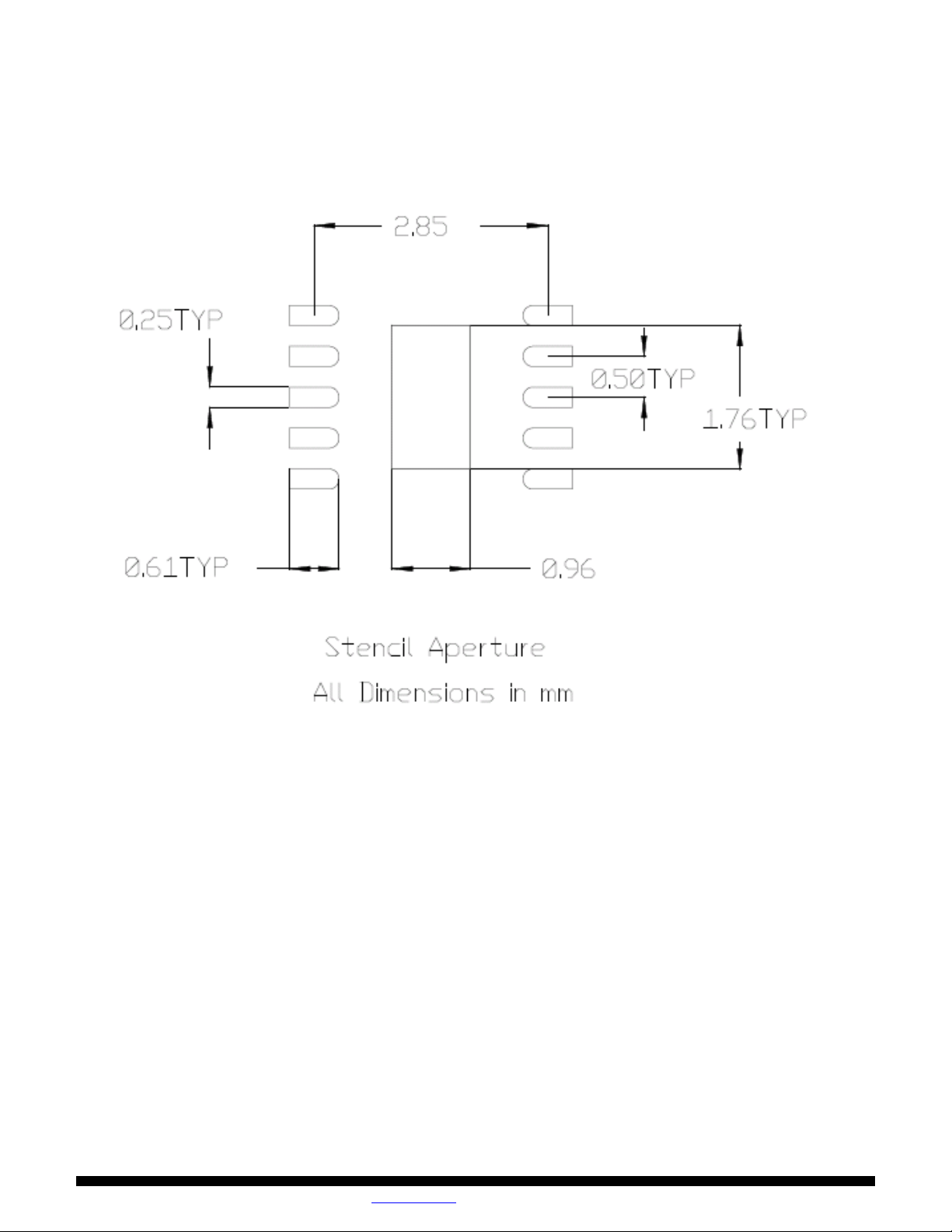
STENCIL DESIGN
Figure 14 below shows a suggested stencil design.
Figure 14 Stencil design
Page 15 of 16 www.irf.com 01/04/08

PACKAGE INFORMATION
3 X 3 MM 10L DFN LEAD FREE
S
Y
M
B
O
L
A 0.80 0.90 1.00 .032 .035 .039
A1 0.00 0.02 0.05 .000 .0008 .0019
A3 0.20REF .008REF
b 0.18 0.25 0.30 .0071 .0098 .0118
D2 2.20 - 2.70 .087 - .106
D 3.00BSC .118BSC
E 3.00BSC .118BSC
E2 1.40 - 1.75 .055 - .068
L 0.30 0.40 0.50 .012 .016 .019
e 0.50 PITCH .020 PITCH
N 10 10
ND 5 5
NE 5 5
aaa 0.15 .0059
bbb 0.10 .0039
ccc 0.10 .0039
ddd 0.05 .0019
MILLIMETERS
MIN NOM MAX MIN NOM MAX
3x3 MLPD
INCHES
Data and specifications subject to change without notice.
This product has been designed and qualified for the Consumer market.
Qualification Standards can be found on IR’s Web site.
IR WORLD HEADQUARTERS: 233 Kansas St., El Segundo, California 90245, USA Tel: (310) 252-7105
TAC Fax: (310) 252-7903
Visit us at www.irf.com for sales contact information.
Page 16 of 16 www.irf.com 01/04/08
 Loading...