International Rectifier IR3507MTRPBF, IR3507 Datasheet
DESCRIPTION
The IR3507 Phase IC combined with an IR XPhase3TM Control IC provides a full featured and flexible way to
implement power solutions for the latest high performance CPUs and ASICs. The “Control” IC provides
overall system control and interfaces with any number of “Phase” ICs which each drive and monitor a single
phase of a multiphase converter. The XPhase3TM architecture results in a power supply that is smaller, less
expensive, and easier to design while providing higher efficiency than conventional approaches.
FEATURES IR3507 PHASE IC
• Power State Indicator (PSI) interface provides the capability to maximize the efficiency at light loads.
• 7V/2A gate drivers (4A GATEL sink current)
• Converter output voltage up to 5.1 V (Limited to VCCL-1.4V)
• Loss-less inductor current sensing
• Feed-forward voltage mode control
• Integrated boot-strap synchronous PFET
• Only four external components per phase
• 3 wire analog bus connects Control and Phase ICs (VID, Error Amp, IOUT)
• 3 wire digital bus for accurate daisy-chain phase timing control without external components
• Anti-bias circuitry prevents excessive sag in output voltage during PSI de-assertion
• PSI input is ignored during power up
• Debugging function isolates phase IC from the converter
• Self-calibration of PWM ramp, current sense amplifier, and current share amplifier
• Single-wire bidirectional average current sharing
• Small thermally enhanced 20L 4 X 4mm MLPQ package
• RoHS compliant
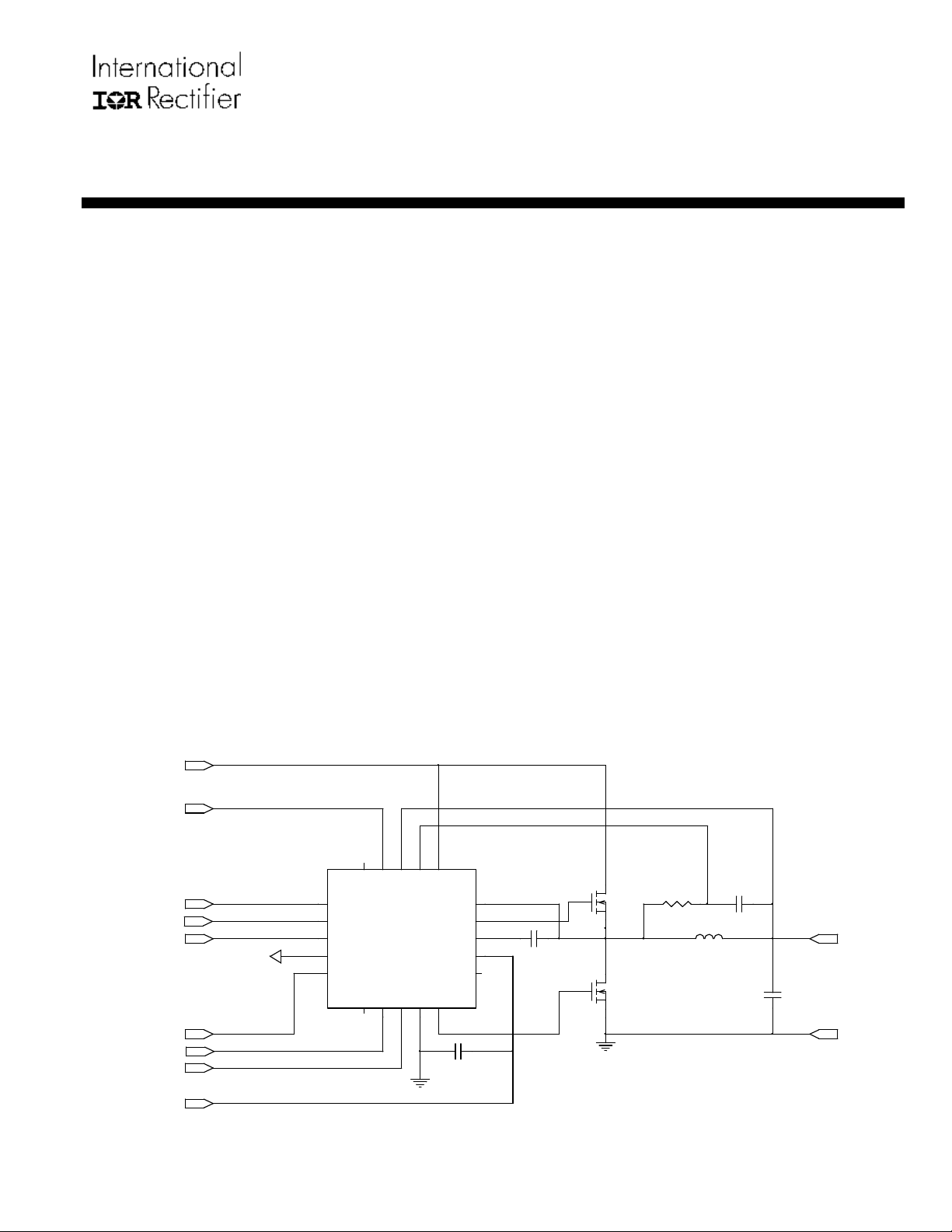
APPLICATION CIRCUIT
IR3507
DATA SHEET
TM
XPHASE3
PHASE IC
12V
EAIN
16
17
19
20
18
IOUT
PSI
DACIN
PHSIN
PHSOUT
CLKIN
VCCL
NC
6
NC
EAIN
IR3507
PHSOUT
7
1
IOUT
2
PSI
3
DACIN
4
LGND
5
PHSIN
VCC
CSIN-
CSIN+
PGND
CLKIN
8
9
GATEH
BOOST
GATEL
10
SW
VCCL
NC
CVCC L
15
14
13
12
CBST
11
RCS
CCS
L
COUT
Figure 1 Application Circuit
Page 1 of 19 Jan 09, 2008
VOUT+
VOUT-
ORDERING INFORMATION
Part Number Package Order Quantity
IR3507MTRPBF 20 Lead MLPQ
* IR3507MPBF 20 Lead MLPQ
* Samples only
ABSOLUTE MAXIMUM RATINGS
Stresses beyond those listed under “Absolute Maximum Ratings” may cause permanent damage to the
device. These are stress ratings only and functional operation of the device at these or any other
conditions beyond those indicated in the operational sections of the specifications are not implied.
Operating Junction Temperature…………….. 0 to 150oC
Storage Temperature Range………………….-65oC to 150oC
MSL Rating………………………………………2
Reflow Temperature…………………………….260oC
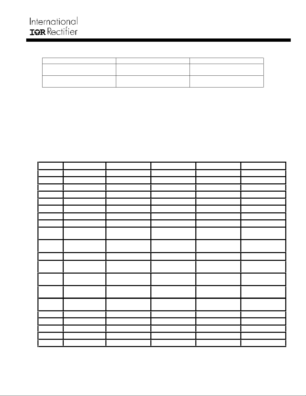
PIN # PIN NAME V
1 IOUT 8V -0.3V 1mA 1mA
2 PSI 8V -0.3V 1mA 1mA
3 DACIN 3.3V -0.3V 1mA 1mA
4 LGND n/a n/a n/a n/a
5 PHSIN 8V -0.3V 1mA 1mA
6 NC n/a n/a n/a n/a
7 PHSOUT 8V -0.3V 2mA 2mA
8 CLKIN 8V -0.3V 1mA 1mA
9 PGND 0.3V -0.3V 5A for 100ns,
10 GATEL 8V -0.3V DC, -5V for
11 NC n/a n/a n/a n/a
12 VCCL 8V -0.3V n/a 5A for 100ns,
13 BOOST 40V -0.3V 1A for 100ns,
14 GATEH 40V -0.3V DC, -5V for
15 SW 34V -0.3V DC, -5V for
16 VCC 34V -0.3V n/a 10mA
17 CSIN+ 8V -0.3V 1mA 1mA
18 CSIN- 8V -0.3V 1mA 1mA
19 EAIN 8V -0.3V 1mA 1mA
20 NC n/a n/a n/a n/a
Note:
1. Maximum GATEH – SW = 8V
2. Maximum BOOST – GATEH = 8V
(4 x 4 mm body)
(4 x 4 mm body)
V
MAX
I
MIN
100ns
100ns
100ns
3000 per reel
100 piece strips
I
SOURCE
200mA DC
5A for 100ns,
200mA DC
100mA DC
3A for 100ns,
100mA DC
3A for 100ns,
100mA DC
IR3507
SINK
n/a
5A for 100ns,
200mA DC
200mA DC
3A for 100ns,
100mA DC
3A for 100ns,
100mA DC
n/a
Page 2 of 19 Jan 09, 2008
IR3507
RECOMMENDED OPERATING CONDITIONS FOR RELIABLE OPERATION WITH MARGIN
8.0V VCC 28V, 4.75V V
7.5V, 0 oC TJ 125 oC. 0.5V 9'$&,19, 500kHz &/.,10+], 250kHz
CCL
3+6,10+]
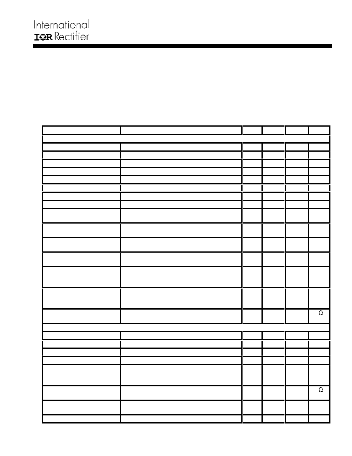
ELECTRICAL CHARACTERISTICS
The electrical characteristics involve the spread of values guaranteed within the recommended operating conditions.
Typical values represent the median values, which are related to 25°C.
C
= 3.3nF, C
GATEH
PARAMETER TEST CONDITION MIN TYP MAX UNIT
Gate Drivers
GATEH Source Resistance BOOST – SW = 7V. Note 1 1.0 2.5
GATEH Sink Resistance BOOST – SW = 7V. Note 1 1.0 2.5
GATEL Source Resistance VCCL – PGND = 7V. Note 1 1.0 2.5
GATEL Sink Resistance VCCL – PGND = 7V. Note 1 0.4 1.0
GATEH Source Current
GATEH Sink Current
GATEL Source Current
GATEL Sink Current
GATEH Rise Time BOOST – SW = 7V, measure 1V to 4V
GATEH Fall Time BOOST – SW = 7V, measure 4V to 1V
GATEL Rise Time VCCL – PGND = 7V, Measure 1V to 4V
GATEL Fall Time VCCL – PGND = 7V, Measure 4V to 1V
GATEL low to GATEH high
delay
GATEH low to GATEL high
delay
Disable Pull-Down
Resistance
Clock
CLKIN Threshold Compare to V(VCCL) 40 45 57 %
CLKIN Bias Current CLKIN = V(VCCL) -0.5 0.0 0.5
CLKIN Phase Delay Measure time from CLKIN<1V to GATEH>1V 40 75 125 ns
PHSIN Threshold Compare to V(VCCL) 35 50 55 %
PHSOUT Propagation
Delay
PHSIN Pull-Down
Resistance
PHSOUT High Voltage I(PHSOUT) = -10mA, measure VCCL –
PHSOUT Low Voltage I(PHSOUT) = 10mA 0.4 1 V
= 6.8nF (unless otherwise specified).
GATEL
BOOST=7V, GATEH=2.5V, SW=0V. 2.0 A
BOOST=7V, GATEH=2.5V, SW=0V. 2.0 A
VCCL=7V, GATEL=2.5V, PGND=0V. 2.0 A
VCCL=7V, GATEL=2.5V, PGND=0V. 4.0 A
transition time
transition time
transition time
transition time
BOOST = VCCL = 7V, SW = PGND = 0V,
measure time from GATEL falling to 1V to
GATEH rising to 1V
BOOST = VCCL = 7V, SW = PGND = 0V,
measure time from GATEH falling to 1V to
GATEL rising to 1V
Note 1 30 80 130 N
Measure time from CLKIN > (VCCL * 50% )
to PHSOUT > (VCCL *50%), 10pF Load
@125oC
30 100 170 N
PHSOUT
5 10 ns
5 10 ns
10 20 ns
5 10 ns
10 20 40 ns
10 20 40 ns
µA
4 15 35 ns
1 0.6 V
Page 3 of 19 Jan 09, 2008
IR3507
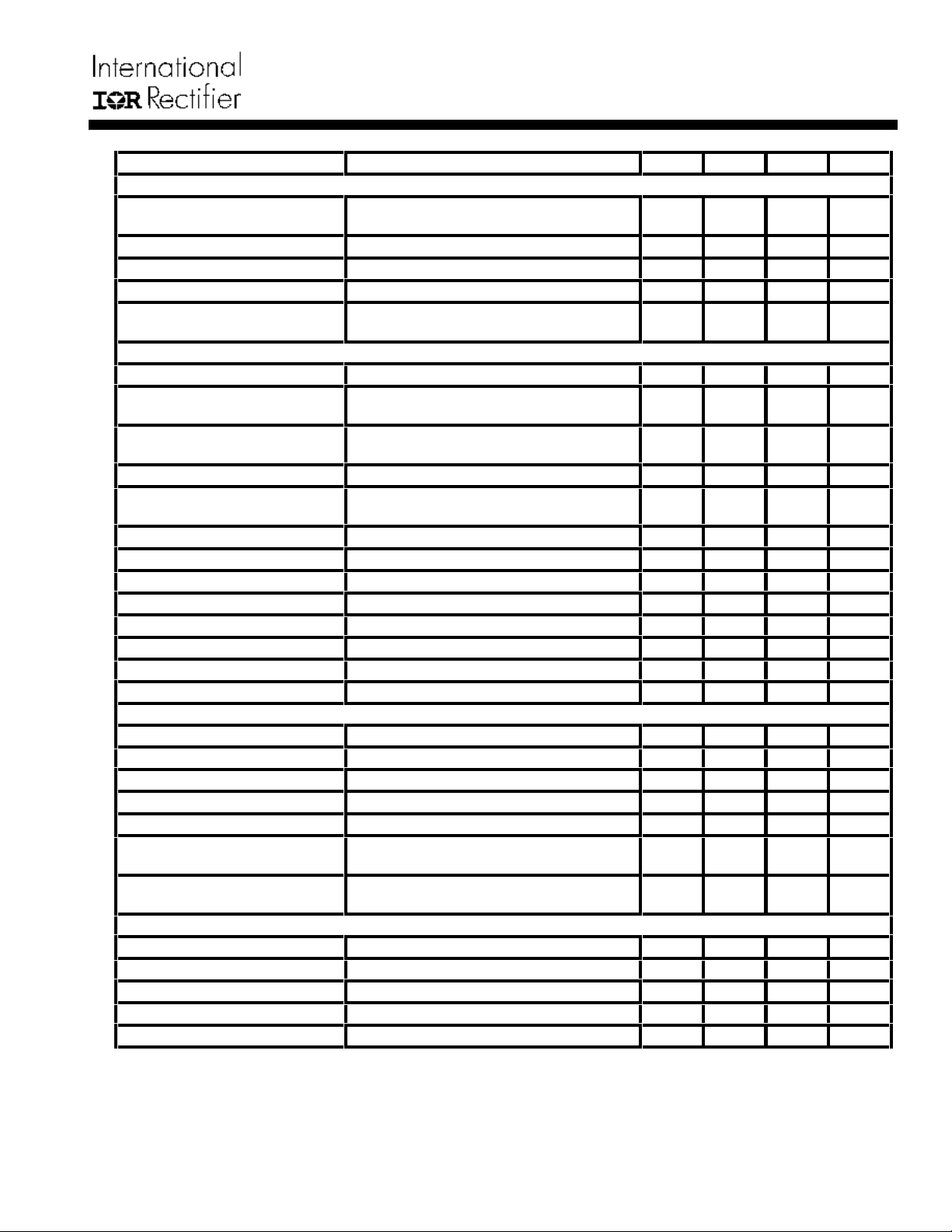
PARAMETER TEST CONDITION MIN TYP MAX UNIT
PWM Comparator
PWM Ramp Slope Vin=12V 42 52.5 57 mV/
%DC
Input Offset Voltage Note 1 -5 0 5 mV
EAIN Bias Current 0 EAIN 3V -5 -0.3 5
Minimum Pulse Width Note 1 55 70 ns
Minimum GATEH Turn-off
Time
Current Sense Amplifier
CSIN+/- Bias Current -200 0 200 nA
CSIN+/- Bias Current
Mismatch
Input Offset Voltage CSIN+ = CSIN- = DACIN. Measure
Gain 0.5V 9'$&,19 30.0 32.5 35.0 V/V
Unity Gain Bandwidth C(IOUT)=10pF. Measure at IOUT.
Slew Rate 6
Differential Input Range 0.8V 9'$&,19, Note 1 -10 50 mV
Differential Input Range 0.5V 9'$&,19, Note 1 -5 50 mV
Common Mode Input Range Note 1 0 Note2 V
Rout at TJ = 25 oC Note 1 2.3 3.0 3.7 k
Rout at TJ = 125 oC 3.6 4.7 5.4 k
IOUT Source Current 0.5 1.6 2.9 mA
IOUT Sink Current 0.5 1.4 2.9 mA
Share Adjust Amplifier
Input Offset Voltage Note 1 -3 0 3 mV
Differential Input Range Note 1 -1 1 V
Gain CSIN+ = CSIN- = DACIN. Note 1 4 5.0 6 V/V
Unity Gain Bandwidth Note 1 4 8.5 17 kHz
PWM Ramp Floor Voltage IOUT Open, Measure relative to DACIN -116 0 116 mV
Maximum PWM Ramp Floor
Voltage
Minimum PWM Ramp Floor
Voltage
PSI Comparator
Rising Threshold Voltage Note 1 520 620 700 mV
Falling Threshold Voltage Note 1 400 550 650 mV
Hysteresis Note 1 50 70 120 mV
Resistance 200 500 850 k
Floating Voltage 800 1150 mV
20 80 160 ns
Note 1 -50 0 50 nA
-1 0 1 mV
input referred offset from DACIN
4.8 6.8 8.8 MHz
Note 1
IOUT = DACIN – 200mV. Measure
relative to floor voltage.
IOUT = DACIN + 200mV. Measure
relative to floor voltage.
120 180 240 mV
-220 -160 -100 mV
µA
V/µs
Page 4 of 19 Jan 09, 2008
IR3507
PARAMETER TEST CONDITION MIN TYP MAX UNIT
Body Brake Comparator
Threshold Voltage with EAIN
decreasing
Threshold Voltage with EAIN
increasing
Hysteresis 70 105 130 mV
Propagation Delay VCCL = 5V. Measure time from EAIN <
OVP Comparator
OVP Threshold Step V(IOUT) up until GATEL drives
Propagation Delay V(VCCL)=5V, Step V(IOUT) up from
Synchronous Rectification Disable Comparator
Threshold Voltage The ratio of V(CSIN-) / V(DACIN), below
Negative Current Comparator
Input Offset Voltage Note 1 -16 0 16 mV
Propagation Delay Time Apply step voltage to V(CSIN+) –
Bootstrap Diode
Forward Voltage I(BOOST) = 30mA, VCCL = 6.8V 360 520 960 mV
Debug Comparator
Threshold Voltage Compare to V(VCCL) -250 -150 -50 mV
General
VCC Supply Current 8V 9(VCC) < 10V 1.1 4.0 6.1 mA
VCC Supply Current 10V 9(VCC) 16V 1.1 2.0 4 mA
VCCL Supply Current 3.1 8.0 12.1 mA
BOOST Supply Current 4.75V 9(BOOST)-V(SW ) 8V 0.5 1.5 3 mA
DACIN Bias Current -1.5 -0.75 1
SW Floating Voltage 0.1 0.3 0.4 V
Note 1: Guaranteed by design, but not tested in production
Note 2: V
-0.5V or VCC – 2.5V, whichever is lower
CCL
Page 5 of 19 Jan 09, 2008
Measure relative to Floor Voltage -300 -200 -110 mV
Measure relative to Floor Voltage -200 -100 -10 mV
V(DACIN) (200mV overdrive) to GATEL
transition to < 4V.
high. Compare to V(VCCL)
V(DACIN) to V(VCCL). Measure time to
V(GATEL)>4V.
which V(GATEL) is always low.
V(CSIN-). Measure time to V(GATEL)<
1V.
40 65 90 ns
-1.0 -0.8 -0.4 V
15 40 70 ns
66 75 86 %
100 200 400 ns
µA
IR3507
PIN DESCRIPTION
PIN# PIN SYMBOL PIN DESCRIPTION
1 IOUT Output of the Current Sense Amplifier is connected to this pin through a 3k
resistor. Voltage on this pin is equal to V(DACIN) + 33 [V(CSIN+) – V(CSIN-)].
Connecting all IOUT pins together creates a share bus which provides an indication
of the average current being supplied by all the phases. The signal is used by the
Control IC for voltage positioning and over-current protection. OVP mode is initiated
if the voltage on this pin rises above V(VCCL)- 0.8V.
2 PSI Logic low is an active low (IE low=low power state).
3 DACIN Reference voltage input from the Control IC. The Current Sense signal and PWM
ramp is referenced to the voltage on this pin.
4 LGND Ground for internal IC circuits. IC substrate is connected to this pin.
5 PHSIN Phase clock input.
6 NC N/A
7 PHSOUT Phase clock output.
8 CLKIN Clock input.
9 PGND Return for low side driver and reference for GATEH non-overlap comparator.
10 GATEL Low-side driver output and input to GATEH non-overlap comparator.
11 NC N/A
12 VCCL Supply for low-side driver. Internal bootstrap synchronous PFET is connected from
this pin to the BOOST pin.
13 BOOST Supply for high-side driver. Internal bootstrap synchronous PFET is connected
between this pin and the VCCL pin.
14 GATEH High-side driver output and input to GATEL non-overlap comparator.
15 SW Return for high-side driver and reference for GATEL non-overlap comparator.
16 VCC Supply for internal IC circuits.
17 CSIN+ Non-Inverting input to the current sense amplifier, and input to debug comparator.
18 CSIN- Inverting input to the current sense amplifier, and input to synchronous rectification
disable comparator.
19 EAIN PWM comparator input from the error amplifier output of Control IC. Body Braking
mode is initiated if the voltage on this pin is less than V(DACIN).
20 NC N/A
Page 6 of 19 Jan 09, 2008
 Loading...