
www.DataSheet4U.com
IR3084U
DESCRIPTION
The IR3084U Control IC combined with an IR XPhase
way to implement a complete VR10, VR11, Opteron, or Athlon64 power solution. The “Control” IC
provides overall system control and interfaces with any number of “Phase” ICs which each drive and
monitor a single phase of a multiphase converter. The XPhase
that is smaller, less expensive, and easier to design while providing higher efficiency than conventional
approaches.
The IR3084U is based on the IR3084 VR10 Control IC, but incorporates the following modifications;
• Supports VR11 7-bit VID, VR10 7-bit extended VID, and Opteron/Athlon64 5-bit VID codes
• Supports both VR11 and legacy Opteron/Athlon64 start-up sequences
• VID Select pin sets the DAC to VR10, VR11, or Opteron/Athlon64
• INTL_MD output pin indicates which DAC is selected – Intel or AMD
• VOSENS float detection protects the CPU in the event that the VOSENS trace is broken
• Enable Input Thresholds set by VID Select pin to either VR10, VR11 or Opteron/Athlon64
• VID Input Thresholds set by VID Select pin to either 0.6V (VR10/VR11) or 1.24V (AMD)
• No-Load Setpoint Current changes polarity based on VID Select to accommodate VR10, VR11
(negative offset from DAC) or Opteron/Athlon64 (positive offset from DAC).
FEATURES
XPHASE
TM
Data Sheet No. PD94719
VR10, VR11 & OPTERON/ATHLON64 CONTROL IC
TM
Phase IC provides a full featured and flexible
TM
architecture results in a power supply
• 1 to X phase operation with matching Phase IC
• 7-bit VR 10/11 compatible VID with 0.5% overall system set point accuracy
• 5-bit Opteron/Athlon64 compatible VID with 1% overall system set point accuracy
• Programmable Dynamic VID Slew Rate
• +/-300mV Differential Remote Sense
• Programmable VID Offset Voltage at the Error Amplifier’s Non-Inverting Input allows Zero Offset
• Programmable 150kHz to 1MHz oscillator
• Programmable VID Offset and Load Line output impedance
• Programmable Hiccup Over-Current Protection with Delay to prevent false triggering
• Simplified VR Ready output provides indication of proper operation and avoids false triggering
• Operates from 12V input with 9.9V Under-Voltage Lockout
• 6.8V/6mA Bias Regulator provides System Reference Voltage
• Phase IC Gate Driver Bias Regulator / VRHOT Comparator
• Reduced Over-Current Detect Delay eliminates and external resistor in typical applications
• Small thermally enhanced 28L MLPQ package
Page 1 of 47 9/14/2005
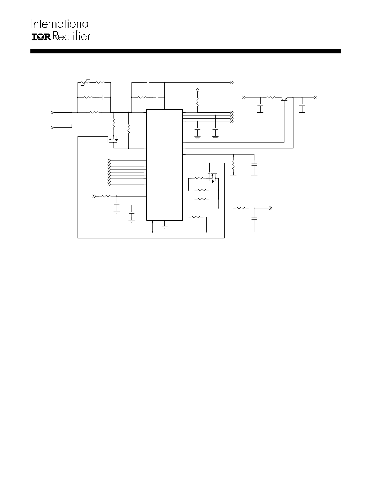
TYPICAL APPLICATION CIRCUIT
CCP1
100pF
R117
RT2
1.21K
VCC_SENSE
VSS_SENSE
4.7K, B=4450
RFB1
162
RFB
348
C1009
1nF
VREG_12V_FI LTERED
CFB
12nF
Q5
OUTEN
VID0
VID1
VID2
VID3
VID4
VID5
VID6
VID_SEL
R30
10
RDRP1
750
C130
0.1uF
RCP
2.49K
RDRP
750
CSS/D EL
0.1uF
17
16
28
9
8
7
6
5
4
3
1
21
26
CCP
56nF
EAOUT
FB
IR3084UMTR
VDRP
ENABLE
VID0
VID1
VID2
VID3
VID4
VID5
VID6
VIDSEL
VCC
SS/DEL
VOSNS--
10
18
LGND
22
VRRDY
RMPOUT
VBIAS
REGDRV
REGFB
REGSET
INTL_MD
VSETPT
OCSET
VDAC
ROSC
U5
IR3084U
VREG_12V_FI LTERED
C89
100pF
Q6
EA
VR_RDY
ISHARE
RMP
VBIAS
RVGDRV
97.6K
RVDAC
3.5
CVGDRV
10nF
CVDAC
33nF
R1331
1
C204
0.1uF
VDAC
Q4
CJD200
C135
1uF
VGDRIVE
+5.0 V
R137
2K
27
15
IIN
19
20
C134
0.1uF
24
23
25
2
RV SETPT1
124
14
RVSETPT
124
13
ROCSET
12.7K
12
11
ROSC
30.1K
Page 2 of 47 9/14/2005
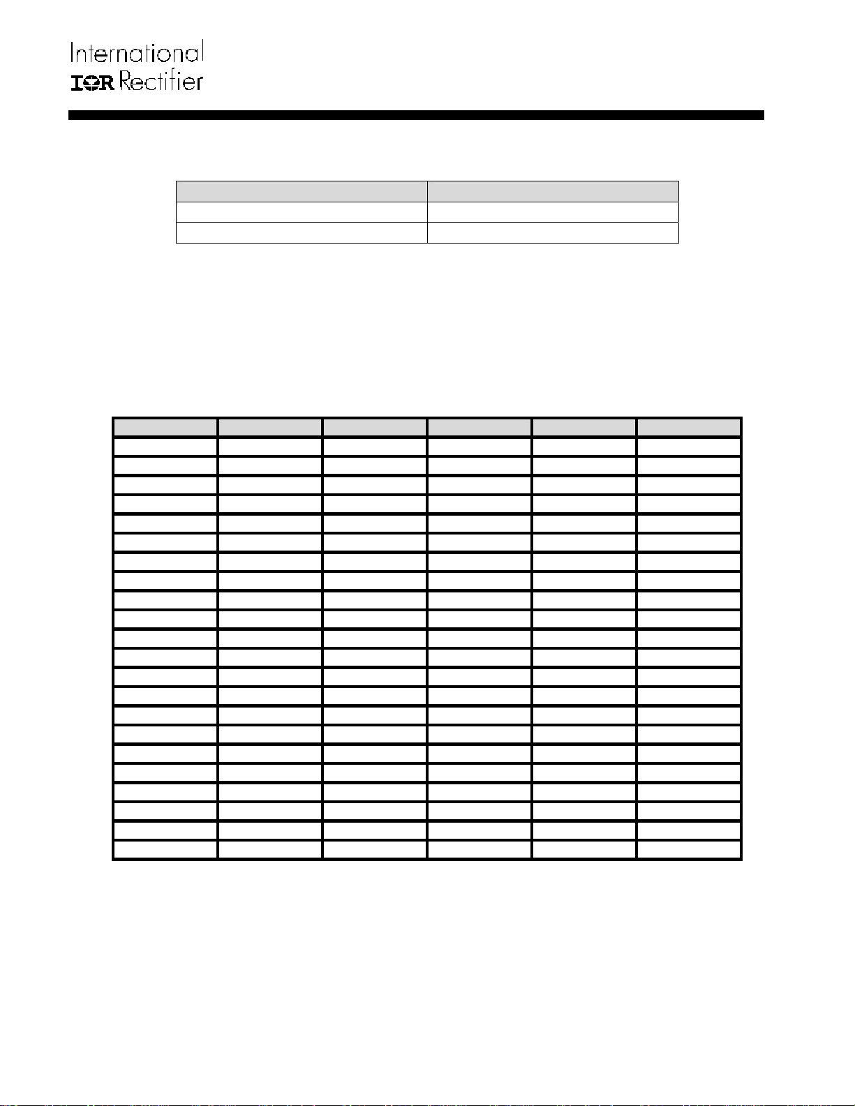
ORDERING INFORAMATION
DEVICE ORDER QUANTITY
IR3084UMTRPBF 3000 Tape and Reel
IR3084UMPBF 100 Piece Strip
ABSOLUTE MAXIMUM RATINGS
IR3084U
Operating Junction Temperature……………..0 to 150oC
Storage Temperature Range………………….65
ESD Rating………………………………………HBM Class 1B JEDEC standard
Moisture Sensitivity Level………………………JEDEC Level 3 @ 260
o
C to 150oC
o
C
PIN # PIN NAME V
V
MAX
I
MIN
SOURCE
I
SINK
1 VIDSEL 20V -0.3V 1mA 1mA
2 INTL_MD 20V -0.3V 1mA 1mA
3-9 VID6VID0 20V -0.3V 1mA 1mA
10 VOSNS- 0.5V -0.5V 10mA 10mA
11 ROSC 20V -0.5V 1mA 1mA
12 VDAC 20V -0.3V 1mA 1mA
13 OCSET 20V -0.3V 1mA 1mA
14 VSETPT 20V -0.3V 1mA 1mA
15 IIN 20V -0.3V 1mA 1mA
16 VDRP 20V -0.3V 5mA 5mA
17 FB 20V -0.3V 1mA 1mA
18 EAOUT 10V -0.3V 20mA 20mA
19 RMPOUT 20V -0.3V 5mA 5mA
20 VBIAS 20V -0.3V 50mA 10mA
21 VCC 20V -0.3V 1mA 50mA
22 LGND n/a n/a 50mA 1mA
23 REGFB 20V -0.3V 1mA 1mA
24 REGDRV 20V -0.3V 10mA 50mA
25 REGSET 20V -0.3V 1mA 1mA
26 SS/DEL 20V -0.3V 1mA 1mA
27 VRRDY 20V -0.3V 1mA 20mA
28 ENABLE 20V -0.3V 1mA 1mA
Page 3 of 47 9/14/2005
IR3084U
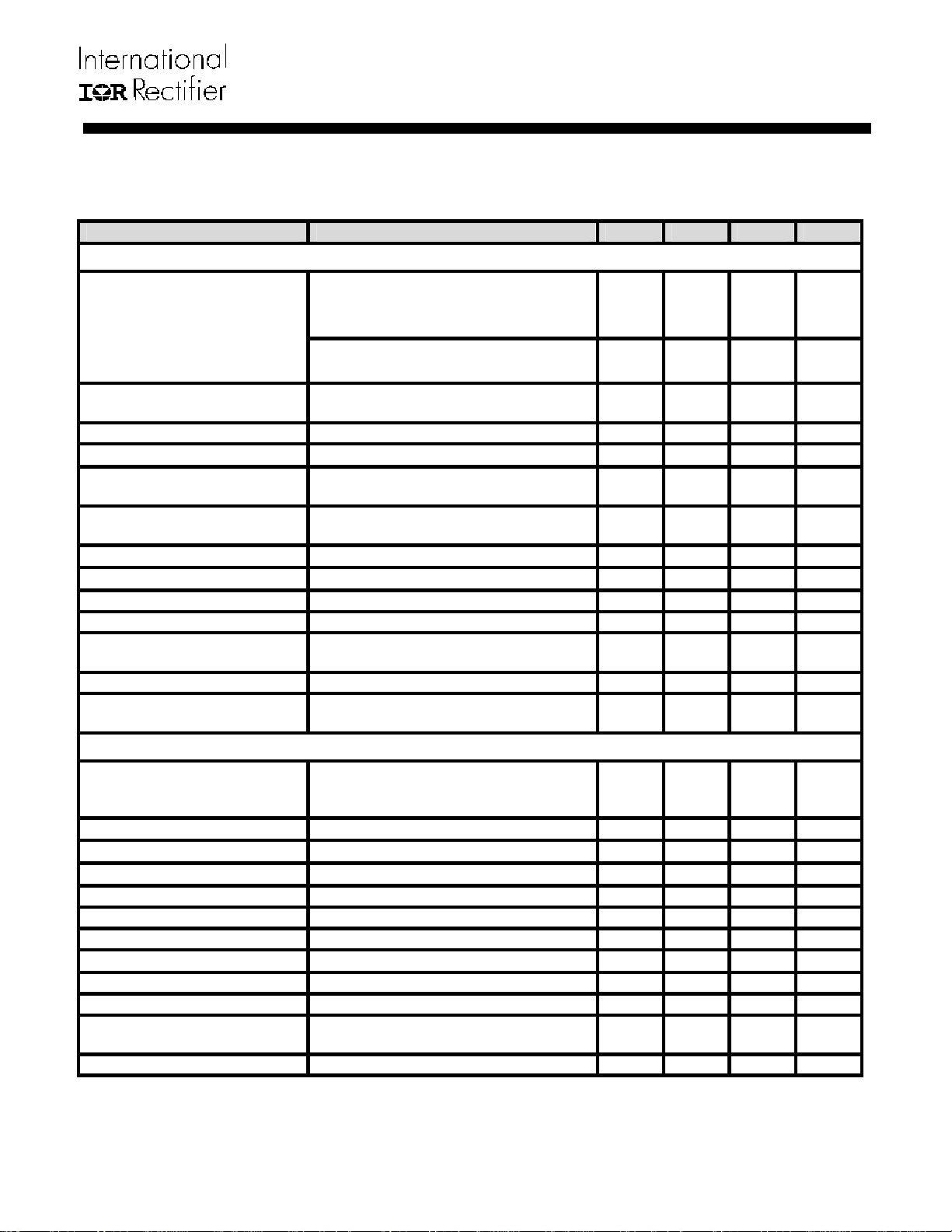
ELECTRICAL SPECIFICATIONS
Unless otherwise specified, these specifications apply over: 9.5V VCC 16V, 0.3V VOSNS- 0.3V,
o
0
C TJ 100 oC, ROSC = 24k, CSS/DEL = 0.1μF ±10%
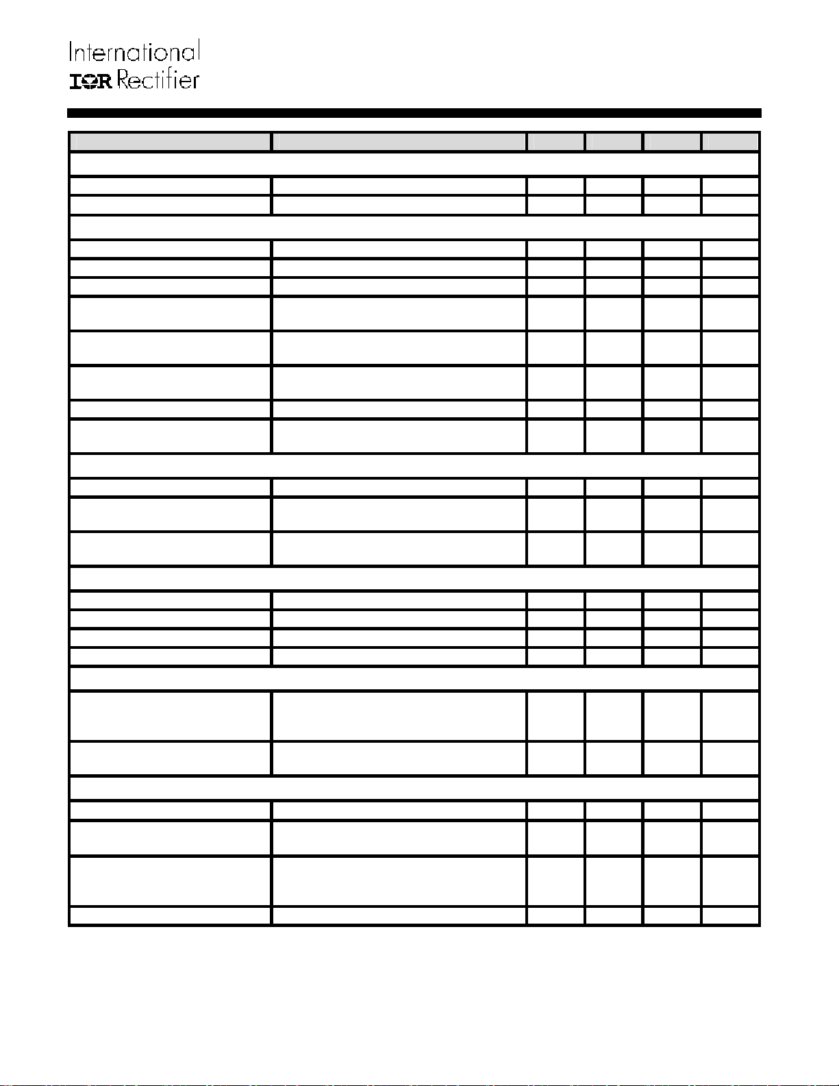
PARAMETER TEST CONDITION MIN TYP MAX UNIT
VDAC REFERENCE
VR10/VR11 System Set-Point
Accuracy (Deviation from
Tables 1 & 2 per test circuit in
VID 1V, 10kROSC100k,
o
C TJ 100 oC
25
0.5 0.5 %
Figure 1 which emulates in-VR
operation)
Opteron/Athlon64 System SetPoint Accuracy
0.8V VID < 1V, 10kROSC100k,
o
C TJ 100 oC
25
o
C TJ 100 oC 1 1 %
25
5 +5 mV
Source Current Includes OCSET and VSETPT currents 104 113 122 A
Sink Current Includes OCSET and VSETPT currents 92 100 108
VR10/VR11 VIDx Input
Threshold
Opteron/Athlon64 VIDx Input
Threshold
VIDx Input Bias Current
500 600 700 mV
1.04 1.24 1.44 V
0V < VIDx < VCC 5 0 5
VIDx 11111x Blanking Delay Measure Time till VRRDY drives low 0.5 1.3 2.1
μA
μA
μs
VIDSEL Pull up Voltage VIDSEL Floating 1.95 2.4 2.85 V
VIDSEL Pull up Resistor 2.25 4.5 9 K
VIDSEL VR10/Opteron
Threshold
VIDSEL “LOW” 0.5 0.6 0.7 V
VIDSEL Opteron Voltage 6.49K from VIDSEL to GND 0.9 1.3 1.7 V
VIDSEL Opteron/VR11
Threshold
1.8 1.95 2.1 V
ERROR AMPLIFIER
Measure V(FB) – V(VSETPT) per test
Input Offset Voltage
circuit in Figure 1. Applies to all VID
5 0.0 5 mV
codes. Note 2.
FB Bias Current 1 0.1 0.5
VSETPT Bias Current VR10/VR11 Mode 48.5 51 53.5
VSETPT Bias Current Opteron/Athlon64 Mode 54 47 39
μA
μA
μA
DC Gain Note 1 90 100 110 dB
Gain Bandwidth Product Note 1 6 10 MHz
Corner Frequency 45 deg Phase Shift, Note 1 200 400 Hz
Slew Rate Note 1 1.4 3.2 5
V/μs
Source Current 1.2 0.7 0.35 mA
Sink Current 0.5 1.1 1.7 mA
Max Voltage
VBIAS–VEAOUT (referenced to
VBIAS)
150 350 600 mV
Min Voltage Normal operation or Fault mode 30 125 200 mV
Page 4 of 47 9/14/2005
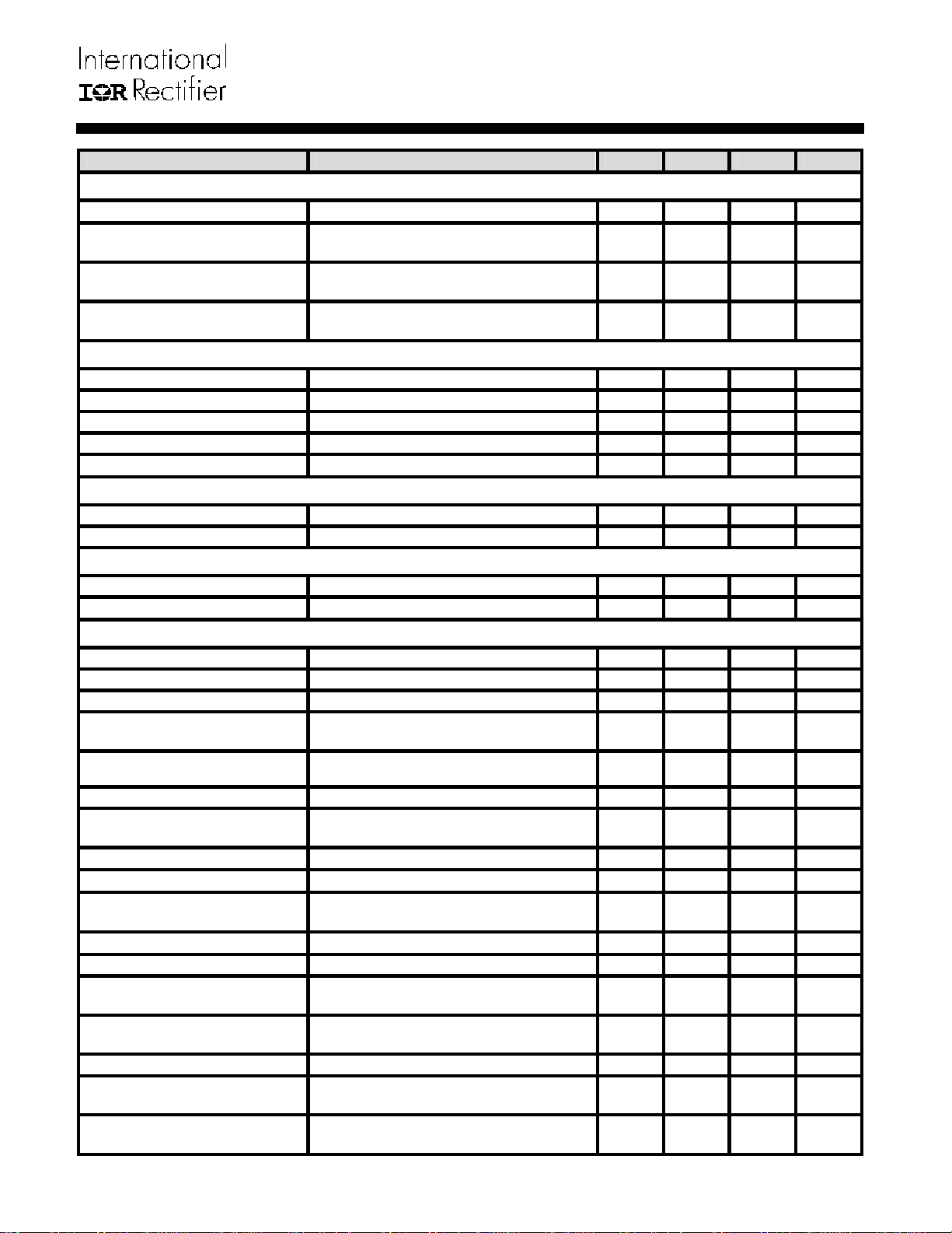
IR3084U
PARAMETER TEST CONDITION MIN TYP MAX UNIT
CURRENT SENSE INPUT
IIN BIAS CURRENT V(SS/DEL) > 0.85V, V(EAOUT) > 0.5V
IIN Preconditioning Pull-Down
Resistance
IIN Preconditioning RESET
Threshold
IIN Preconditioning SET
Threshold
VDRP BUFFER AMPLIFIER
Input Offset Voltage V(VDRP) – V(IIN), 0.5V < V(IIN) < 5V 10 2 6 mV
Source Current 0.5V < V(IIN) < 5V 9.0 6.8 4.0 mA
Sink Current 0.5V < V(IIN) < 5V 0.2 0.85 4.1 mA
Bandwidth (-3dB) Note 1 1 6 MHz
Slew Rate Note 1 5 10
VBIAS REGULATOR
Output Voltage 5mA < I(VBIAS) < 0mA 6.6 6.9 7.2 V
Current Limit 35 20 6 mA
OVER-CURRENT COMPARATOR
Input Offset Voltage 1V < V(OCSET) < 5V 10 0 10 mV
OCSET Bias Current 53.5 51 48.5
SOFT START AND DELAY
Start Delay (TD1) RDRP = 1.2 1.8 2.6 ms
Soft Start Time (TD2) RDRP = , Time to reach 1.1V 0.8 1.8 2.8 ms
VID Sample Delay (TD3) VR10/VR11 mode only 0.2 1.0 2.5 ms
DVID Slew Time & VRRDY
Delay (TD4+TD5)
PowerGood Delay
OC Delay Time 150 250 350 us
SS/DEL to FB Input Offset
Voltage
SS/DEL Charge Current
SS/DEL Discharge Current
Charge/Discharge Current
Ratio
OC Discharge Current Note 1
Charge Voltage 3.6 3.85 4.1 V
OC/VRRDY Delay Comparator
Threshold
OC/VRRDY Delay Comparator
Threshold
Delay Comparator Hysteresis Note 1 20 mV
VID Sample Delay
Comparator Threshold
SS/DEL Discharge
Comparator Threshold
V(SS/DEL) < 0.35V 5.6 12.5 19.4 K
V(EAOUT) 0.20 0.35 0.50 V
V(SS/DEL) 0.35 0.60 0.85 V
VR10/VR11 mode only 0.5 1.3 2.2 ms
Opteron/Athlon64 mode. Measured from
Vcore=1.1V to when VRRDY transitions HI.
With FB = 0V, adjust V(SS/DEL) until
EAOUT drives high
Relative to Charge Voltage, SS/DEL
rising
Relative to Charge Voltage, SS/DEL
falling
VR10/VR11 mode only 3.10 V
215 mV
2.0 0.2 1.0
0.7 2.3 4.7 ms
0.85 1.3 1.5 V
40 70 100
4 6.5 9
9.5 11.2 12.5
20 40 60
80 mV
100 mV
µA
V/μs
μA
μA
μA
μA/μA
μA
Page 5 of 47 9/14/2005
IR3084U
PARAMETER TEST CONDITION MIN TYP MAX UNIT
VRRDY OUTPUT
Output Voltage I(VRRDY) = 4mA 150 300 mV
Leakage Current V(VRRDY) = 5.5V 0 10
ENABLE INPUT
VR10/11 Threshold Voltage ENABLE rising 800 850 900 mV
VR10/11 Threshold Voltage ENABLE falling 700 750 800 mV
VR10/11 Threshold Hysteresis 70 100 130 mV
Opteron/Athlon64 Threshold
Voltage
Opteron/Athlon64 Threshold
Voltage
Opteron/Athlon64 Threshold
Hysteresis
Input Resistance 50 100 200 K
Blanking Time
OSCILLATOR
Switching Frequency ROSC = 24K 450 500 550 kHz
Peak Voltage (4.8V typical,
measured as % of VBIAS)
Valley Voltage (0.9V typical,
measured as % of VBIAS)
INTL_MD OUTPUT
Source Current V(INTL_MD)=2V, VR10 or VR11 mode 100 200 300 µA
Sink Current V(INTL_MD)=2V, Opteron mode 250 750 1500 µA
Max Voltage Pin Floating, V(VBIAS)V(INTL_MD) 50 170 350 mV
Min Voltage Pin Floating, LGND referenced 400 900 mV
VOSNS− FLOAT DETECT
Detect Voltage
Detect Delay
DRIVER BIAS REGULATOR
REGSET Bias Current 1.5V < V(REGSET) < VCC – 1.5V 112 99 85
Input Offset Voltage
Short Circuit Current
Dropout Voltage I(REGDRV) = 10mA, Note 1 0.4 0.87 1.33 V
ENABLE rising 1.11 1.23 1.35 V
ENABLE falling 1.06 1.17 1.29 V
35 60 85 mV
Noise Pulse < 250ns will not register
an ENABLE state change. Note 1
70 71 74 %
10 13 15 %
V(VOSNS) with respect to V(LGND),
Verify V(VRRDY) and V(EAOUT) are
low.
V(VOSNS-) 0V to 2.6V step, measure
time when V(VRRDY) falls. Note 1
1.5V < V(REGSET) < VCC – 1.5V,
100μA < I(REGDRV) < 10mA
V(REGDRV) = 0V,
1.5V < V(REGSET) < VCC – 1.5V,
Note 1
μA
75 250 400 ns
1.2 2 2.6 V
200 350 600 ns
μA
12 0 12 mV
10 20 50 mA
Page 6 of 47 9/14/2005
IR3084U
PARAMETER TEST CONDITION MIN TYP MAX UNIT
VCC UNDER-VOLTAGE LOCKOUT
Start Threshold 9.3 9.9 10.3 V
Stop Threshold 8.5 9.1 9.5 V
Hysteresis Start – Stop 550 800 1000 mV
GENERAL
VCC Supply Current 9 14 18 mA
VOSNS Current
0.3V < VOSNS < 0.3V,
All VID Codes
Note 1: Guaranteed by design, but not tested in production
Note 2: VDAC Output is trimmed to compensate for Error Amp input offsets errors
1.45 1.1 0.75 mA
IR3084U
+
"FAST"
VDAC
-
+
200 OHM
VDAC
-
+
BUFFER
AMP
ISOURCE
ISINK
INTEL: +IOFFSET
AMD: --IOFFSET
IROSC IROSC
-
ERROR
AMP
EAOUT
VSETPT
OCSET
IOCSET
FB
VDAC
RVDAC
200 OHM
SYSTEM
SET POINT
VOLTAGE
CVDAC
ROSC
CURRENT
SOURCE
GENERATOR
ROSC
BUFFER
AMP
+
-
ROSC
+
1.2V
-
VOSNS-
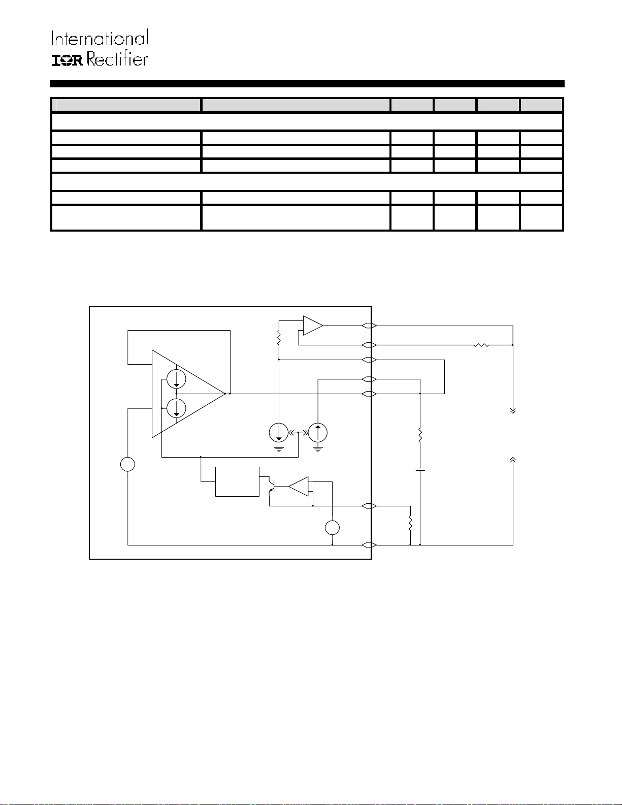
Figure 1 – System Set Point Test Circuit
Page 7 of 47 9/14/2005
PIN DESCRIPTIONS
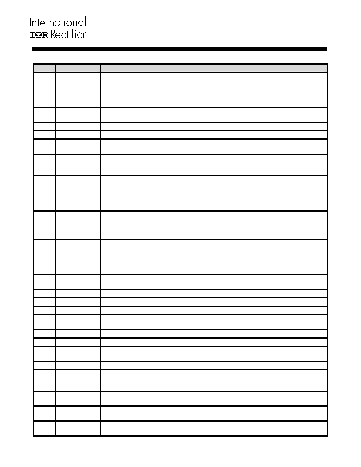
PIN# PIN SYMBOL DESCRIPTION
Selects the DAC table and the type of Soft Start. There are 3 possible modes of
operation: (1) GND selects VR10 DAC and VR11 type startup, (2) FLOAT (2.4V)
1 VIDSEL
2 INTL_MD
3-9 VID6VID0
10 VOSNS
11 ROSC
12 VDAC
13 OCSET
14 VSETPT
15 IIN
16 VDRP
17 FB
18 EAOUT
19 RMPOUT
20 VBIAS
21 VCC
22 LGND
23 REGFB
24 REGDRV
25 REGSET
26 SS/DEL
27 VRRDY
28 ENABLE
selects VR11 DAC and VR11 type startup, (3) 6.49K to GND (1.3V) selects
Opteron/Athlon64 DAC and legacy type startup. Additional details are provided in
the Theory of Operation section.
Output that indicates if the controller is in Intel Mode or AMD Mode. This pin will be
Low when in AMD mode and High when in Intel mode.
Inputs to the D to A Converter. Must be connected to an external pull up resistor.
Negative Remote Sense Input. Connect to ground at the Load.
Connect a resistor from this pin to VOSNS to program the oscillator’s frequency,
OCSET, VSETPT, REGSET, and VDAC bias currents.
Regulated output voltage programmed by the VID inputs. Connect an external RC
network to from this pin to VOSNS to program the Dynamic VID slew rate and
provide compensation for the internal Buffer Amplifier.
Programs the hiccup over-current threshold through an external resistor tied to
VDAC and an internal current source. Over-current protection can be disabled by
connecting a resistor from this pin to VDAC to program the threshold higher than the
possible signal into the IIN pin from the Phase ICs but no greater than 5V (do not
float this pin as improper operation will occur).
Error Amp non-inverting input. The converter’s output voltage can be decreased
(Intel) or increased (AMD) from the VDAC voltage with an external resistor
connected between VDAC and an internal current source. Current sensing and
PWM operation are referenced to this pin.
Current Sense input from the Phase IC(s). Prior to startup, when SS/DEL<0.6V, this
pin is pulled low by a 12.5K resistor to disable current balancing in the Phase ICs.
When SS/DEL>0.6V and EAOUT>0.35V, this pin is released and current balancing
is enabled. If AVP or over-current protection is not required, connect this pin to
VDAC. To ensure proper do not float this pin.
Buffered IIN signal. Connect an external resistor from this pin to the FB pin to set the
converter’s output impedance.
Inverting input to the Error Amplifier.
Output of the Error Amplifier. When Low, provides UVL function to the Phase ICs.
Oscillator Output voltage. Used by the Phase ICs to program Phase Delay.
6.9V/6mA Regulated output used as a system reference voltage for internal circuitry
and for phase timing at the Phase ICs.
Power Input for the internal circuitry.
Local Ground for internal circuitry and IC substrate connection
Inverting input of the Bias Regulator Error Amp. Connect this pin to the collector of
the Phase IC Gate Driver Bias transistor.
Output of the Bias Regulator Error Amp.
Non-inverting input of the Bias Regulator Error Amp. The output voltage of the
Phase IC Gate Driver Bias Regulator is set by an internal current source supplying
an external resistor connected from this pin to ground.
Controls converter start-up and over-current timing. Connect an external capacitor
from this pin to LGND to program the soft start and delay times.
Open Collector output that drives low during start-up and when any external fault
occurs. Connect external pull-up resistor.
Enable Input. A logic low applied to this pin puts the IC into Fault mode. This pin
has a 100K pull-down resistor to GND.
IR3084U
Page 8 of 47 9/14/2005
IR3084U
SYSTEM THEORY OF OPERATION
XPhaseTM Architecture
The XPhase
applications requiring small size, design flexibility, low voltage, high current and fast transient response. The
architecture can be used in any multiphase converter ranging from 1 to 16 or more phases where flexibility
facilitates the design trade-off of multiphase converters. The scalable architecture can be applied to other
applications which require high current or multiple output voltages.
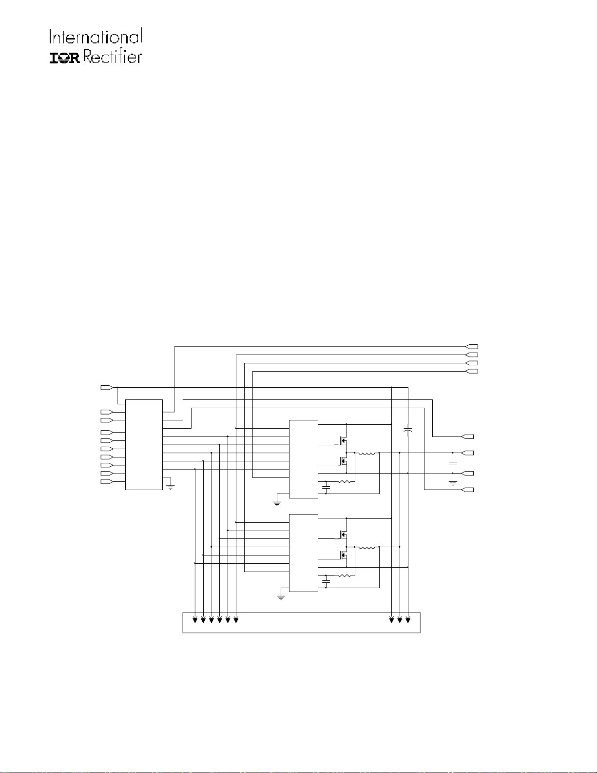
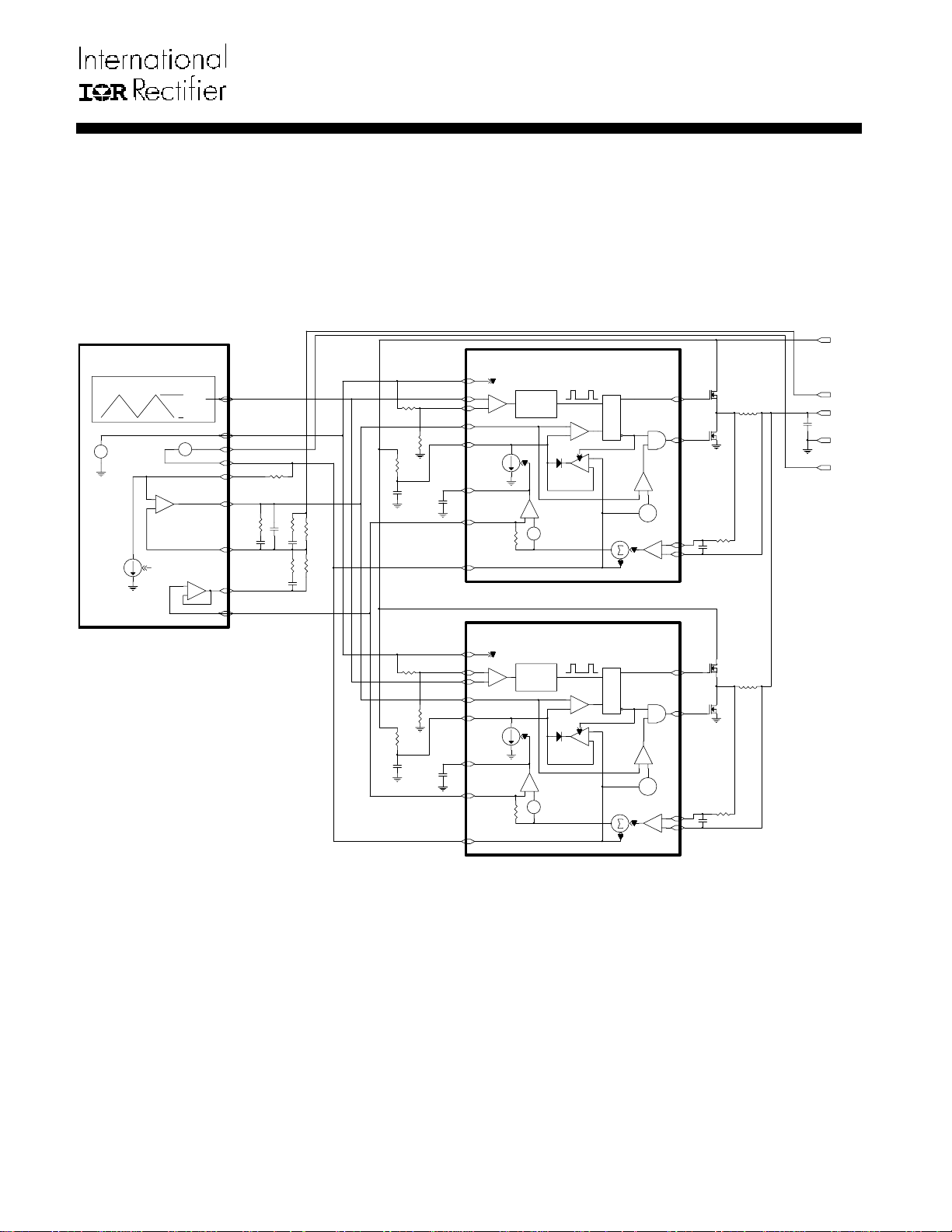
As shown in Figure 2, the XPhase
converters each using a single Phase IC. The Control IC communicates with the Phase ICs through a 5-wire
analog bus, i.e. bias voltage, phase timing, average current, error amplifier output, and VID voltage. The Control
IC incorporates all the system functions, i.e. VID, PWM ramp oscillator, error amplifier, bias voltage, and fault
protections etc. The Phase IC implements the functions required by the converter of each phase, i.e. the gate
drivers, PWM comparator and latch, over-voltage protection, and current sensing and sharing.
There is no unused or redundant silicon with the XPhase
controller that can be configured for 2, 3, or 4 phase operation. PCB Layout is easier since the 5 wire bus
eliminates the need for point-to-point wiring between the Control IC and each Phase. The critical gate drive and
current sense connections are short and local to the Phase ICs. This improves the PCB layout by lowering the
parasitic inductance of the gate drive circuits and reducing the noise of the current sense signal.
TM
architecture is designed for multiphase interleaved buck converters which are used in
TM
architecture consists of a Control IC and a scalable array of phase
TM
architecture compared to others such as a 4 phase
VR READY
PHASE FAULT
VR HOT
VR FAN
12V
ENABLE
VIDSEL
VID6
VID5
VID4
VID3
VID2
VID1
VID0
IR3084
CONTROL
IC
>> BIAS VOLTAGE
>> PHASE TIMING
<< CURRENT SENSE
>> PWM CONTROL
>> VID VOLTAGE
PHASE FAULT
CURRENT SHARE
PHASE FAULT
CURRENT SHARE
IR3086
PHASE
IC
CCS
IR3086
PHASE
IC
ADDITIONAL PHASES
RCS
RCSCCS
Figure 2 – System Block Diagram
CIN
COUT
INPUT/OUTPUTCONTROL BUS
VOUT SENSE+
VOUT+
VOUT-
VOUT SENSE-
Page 9 of 47 9/14/2005
IR3084U
PWM Control Method
The PWM block diagram of the XPhase
with trailing edge modulation is used. A high-gain wide-bandwidth voltage type error amplifier in the Control IC is
used for the voltage control loop. An external RC circuit connected to the input voltage and ground is used to
program the slope of the PWM ramp and to provide the feed-forward control at each phase. The PWM ramp
slope will change with the input voltage and automatically compensate for changes in the input voltage. The input
voltage can change due to variations in the silver box output voltage or due to drops in the PCB related to
changes in load current.
CONTROL IC
50%
RAMP GE NERATOR
DUTY
CYCLE
+
-
IOFFSET
VBIAS
REGULATOR
+
-
IROSC
ERROR
AMP
VPEAK
VVALLEY
VDAC
+
RMPOUT
VBIAS
VOSNS-
-
VDAC
VSETPT
RVSETPT
EAOUT
FB
VDRP
AMP
+
VDRP
-
IIN
TM
architecture is shown in Figure 3. Feed-forward voltage mode control
VIN
CLOCK
PULSE
GENERATOR
+
-
+
-
CLOCK
PULSE
GENERATOR
+
-
+
-
20mV
20mV
RAMP
DISCHARGE
CLAMP
RAMP
DISCHARGE
CLAMP
PHASE IC
PWM
COMPARATOR
-
+
ENABLE
+
-
PHASE IC
PWM
COMPARATOR
-
+
ENABLE
+
-
PWM
LATCH
S
RESET
DOMINANT
R
O% DUTY
CYCLE
COMPARATOR
PWM
LATCH
S
RESET
DOMINANT
R
O% DUTY
CYCLE
COMPARATOR
GATEH
GATELEAIN
+
-
X
0.91
CURRENT
SENSE
AMP
X34
+
CURRENT
SENSE
AMP
X34
CSIN+
+
-
-
X
0.91
+
-
CSIN-
GATEH
GATEL
CSIN+
CSIN-
CCS
CCS RCS
RCS
VOSNS+RAMPIN+
VOUT
COUT
GND
VOSNS-
RAMP
SLOPE
ADJUST
RAMP
SLOPE
ADJUST
SYSTEM
REFERENCE
VOLTAGE
+
-
SHARE
ADJUST
ERROR
AMP
10K
SYSTEM
REFERENCE
VOLTAGE
+
-
SHARE
ADJUST
ERROR
AMP
10K
BIASIN
RRAMP1
RAMPIN-
RRAMP2
PWMRMP
RPWMRMP
SCOMP
CPWMRMP
CSCOMP
RVFB
RDRP
RRAMP1
RRAMP2
RPWMRMP
CPWMRMP
ISHARE
DACIN
BIASIN
RAMPIN+
RAMPIN-
EAIN
PWMRMP
SCOMP
CSCOMP
ISHARE
DACIN
Figure 3 – IR3084U PWM Block Diagram
Frequency and Phase Timing Control
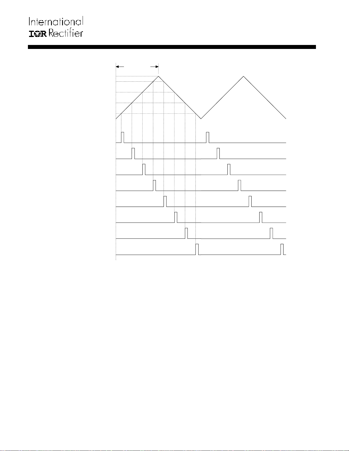
The oscillator is located in the Control IC and its frequency is programmable from 150kHz to 1MHZ by an external
resistor. The output of the oscillator is a 50% duty cycle triangle waveform with peak and valley voltages of
approximately 5V and 1V. This signal is used to program both the switching frequency and phase timing of the
Phase ICs. The Phase IC is programmed by resistor divider RRAMP1 and RRAMP2 connected between the
VBIAS reference voltage and the Phase IC LGND pin. A comparator in the Phase ICs detects the crossing of the
oscillator waveform with the voltage generated by the resistor divider and triggers a clock pulse that starts the
PWM cycle. The peak and valley voltages track the VBIAS voltage reducing potential Phase IC timing errors.
Figure 4 shows the Phase timing for an 8 phase converter. Note that both slopes of the triangle waveform can be
used for synchronization by swapping the RAMP + and – pins.
Page 10 of 47 9/14/2005
RAMP (FROM
VPEAK (5.0V)
VPHASE4&5 (4.5V)
VPHASE3&6 (3.5V)
VPHASE2&7 (2.5V)
VPHASE1&8 (1.5V)
VVALLEY (1.00V)
CONTROL IC)
CLK1
CLK2
CLK3
CLK4
50% RAMP
DUTY CYCLE
IR3084U
SLOPE = 80mV / % DC
SLOPE = 1.6mV / ns @ 200kHz
SLOPE = 8.0mV / ns @ 1MHz
CLK5
CLK6
CLK7
PHASE IC CLOCK PULSES
CLK8
Figure 4 – 8 Phase Oscillator Waveforms
PWM Operation
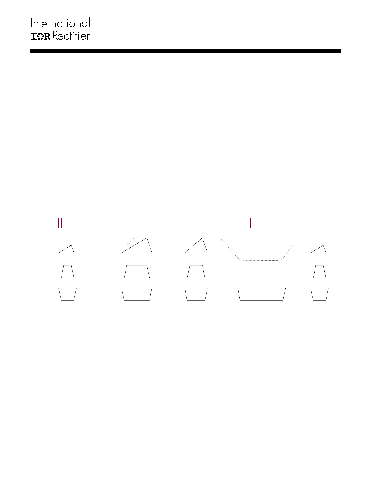
The PWM comparator is located in the Phase IC. Upon receiving a clock pulse, the PWM latch is set, the
PWMRMP voltage begins to increase, the low side driver is turned off, and the high side driver is then turned on.
When the PWMRMP voltage exceeds the Error Amp’s output voltage the PWM latch is reset. This turns off the
high side driver, turns on the low side driver, and activates the Ramp Discharge Clamp. The clamp quickly
discharges the PWMRMP capacitor to the VDAC voltage of the Control IC until the next clock pulse.
The PWM latch is reset dominant allowing all phases to go to zero duty cycle within a few tens of nanoseconds in
response to a load step decrease. Phases can overlap and go to 100% duty cycle in response to a load step
increase with turn-on gated by the clock pulses. An Error Amp output voltage greater than the common mode
input range of the PWM comparator results in 100% duty cycle regardless of the voltage of the PWM ramp. This
arrangement guarantees the Error Amp is always in control and can demand 0 to 100% duty cycle as required. It
also favors response to a load step decrease which is appropriate given the low output to input voltage ratio of
most systems. The inductor current will increase much more rapidly than decrease in response to load transients.
This control method is designed to provide “single cycle transient response” where the inductor current changes
in response to load transients within a single switching cycle maximizing the effectiveness of the power train and
minimizing the output capacitor requirements. An additional advantage is that differences in ground or input
voltage at the phases have no effect on operation since the PWM ramps are referenced to VDAC.
Page 11 of 47 9/14/2005
IR3084U
Body Braking
In a conventional synchronous buck converter, the minimum time required to reduce the current in the inductor in
response to a load step decrease is;
The slew rate of the inductor current can be significantly increased by turning off the synchronous rectifier in
response to a load step decrease. The switch node voltage is then forced to decrease until conduction of the
synchronous rectifier’s body diode occurs. This increases the voltage across the inductor from Vout to Vout +
V
BODY DIODE
decrease is now;
Since the voltage drop in the body diode is often higher than output voltage, the inductor current slew rate can be
increased by 2X or more. This patent pending technique is referred to as “body braking” and is accomplished
through the “0% Duty Cycle Comparator” located in the Phase IC. If the Error Amp’s output voltage drops below
91% of the VDAC voltage this comparator turns off the low side gate driver.
Figure 5 depicts PWM operating waveforms under various conditions
PHASE IC
CLOCK
PULSE
TM
T
SLEW
= [L x (I
MAX
- I
)] / Vout
MIN
. The minimum time required to reduce the current in the inductor in response to a load transient
T
SLEW
= [L x (I
MAX
- I
MIN
)] / (Vout + V
BODY DIODE
)
EAIN
PWMRMP
GATEH
GATEL
VDAC
STEADY-STATE
OPERATION
DUTY CYCLE INCREASE
DUE TO LOAD
INCREASE
DUTY CYCLE DECREASE
DUE TO VIN INCREASE
(FEED-FORWARD)
BODY BRAKING
THRESHOLD
DUTY CYCLE DECREASE DUE TO LOAD
DECREASE (BODY BRAKING) OR FAULT
(VCC UV, VCCVID UV, OCP, VID=11111X)
STEADY-STATE
OPERATION
Figure 5 – PWM Operating Waveforms
Lossless Average Inductor Current Sensing
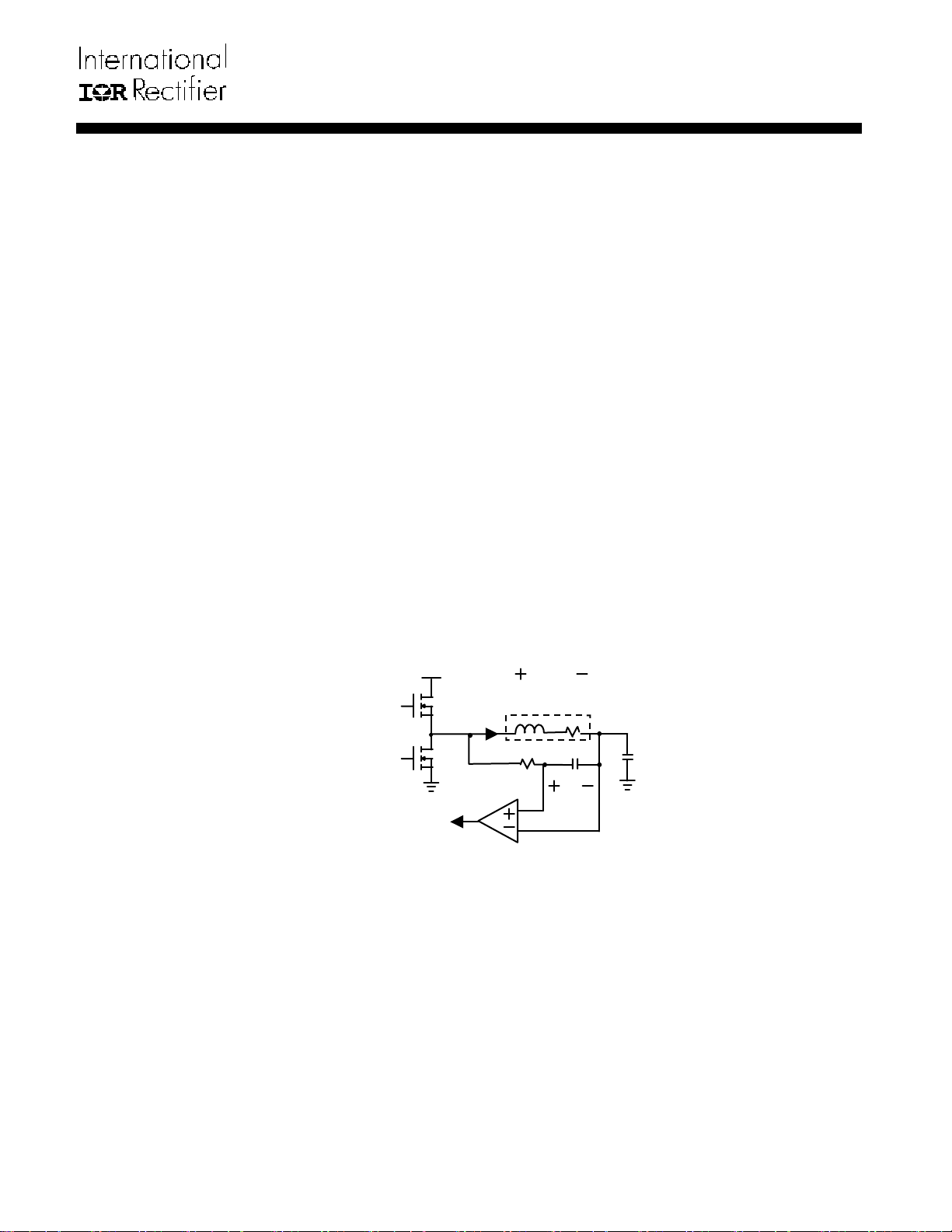
Inductor current can be sensed by connecting a series resistor and a capacitor network in parallel with the
inductor and measuring the voltage across the capacitor. The equation of the sensing network is,
sLR
svsv
=
LC
1
)()(
1
CsR
+
SS
si
=
L
+
L
)(
+
1
CsR
SS
Usually the resistor Rcs and capacitor Ccs are chosen so that the time constant of Rcs and Ccs equals the time
constant of the inductor which is the inductance L over the inductor DCR. If the two time constants match, the
voltage across Ccs is proportional to the current through L, and the sense circuit can be treated as if only a sense
resistor with the value of R
L was used. The mismatch of the time constants does not affect the measurement of
inductor DC current, but affects the AC component of the inductor current.
Page 12 of 47 9/14/2005
IR3084U
The advantage of sensing the inductor current versus high side or low side sensing is that actual output current
being delivered to the load is obtained rather than peak or sampled information about the switch currents. The
output voltage can be positioned to meet a load line based on real time information. Except for a sense resistor in
series with the inductor, this is the only sense method that can support a single cycle transient response. Other
methods provide no information during either load increase (low side sensing) or load decrease (high side
sensing).
An additional problem associated with peak or valley current mode control for voltage positioning is that they
suffer from peak-to-average errors. These errors will show in many ways but one example is the effect of
frequency variation. If the frequency of a particular unit is 10% low, the peak to peak inductor current will be 10%
larger and the output impedance of the converter will drop by about 10%. Variations in inductance, current sense
amplifier bandwidth, PWM prop delay, any added slope compensation, input voltage, and output voltage are all
additional sources of peak-to-average errors.
Current Sense Amplifier
A high speed differential current sense amplifier is located in the Phase IC, as shown in Figure 6. Its gain
decreases with increasing temperature and is nominally 34 at 25ºC and 29 at 125ºC (-1470 ppm/ºC). This
reduction of gain tends to compensate the 3850 ppm/ºC increase in inductor DCR. Since in most designs the
Phase IC junction is hotter than the inductor these two effects tend to cancel such that no additional temperature
compensation of the load line is required.
The current sense amplifier can accept positive differential input up to 100mV and negative up to -20mV before
clipping. The output of the current sense amplifier is summed with the DAC voltage and sent to the Control IC
and other Phases through an on-chip 10K resistor connected to the ISHARE pin. The ISHARE pins of all the
phases are tied together and the voltage on the share bus represents the average inductor current through all the
inductors and is used by the Control IC for voltage positioning and current limit protection.
vL
LRL
iL
Rs Cs
CSA
CO
Figure 6 – Inductor Current Sensing and Current Sense Amplifier
Average Current Share Loop
Current sharing between phases of the converter is achieved by the average current share loop in each Phase
IC. The output of the current sense amplifier is compared with the share bus less a 20mV offset. If current in a
phase is smaller than the average current, the share adjust amplifier of the phase will activate a current source
that reduces the slope of its PWM ramp thereby increasing its duty cycle and output current. The crossover
frequency of the current share loop can be programmed with a capacitor at the SCOMP pin so that the share loop
does not interact with the output voltage loop.
vc
Vo
Co
Page 13 of 47 9/14/2005
IR3084U
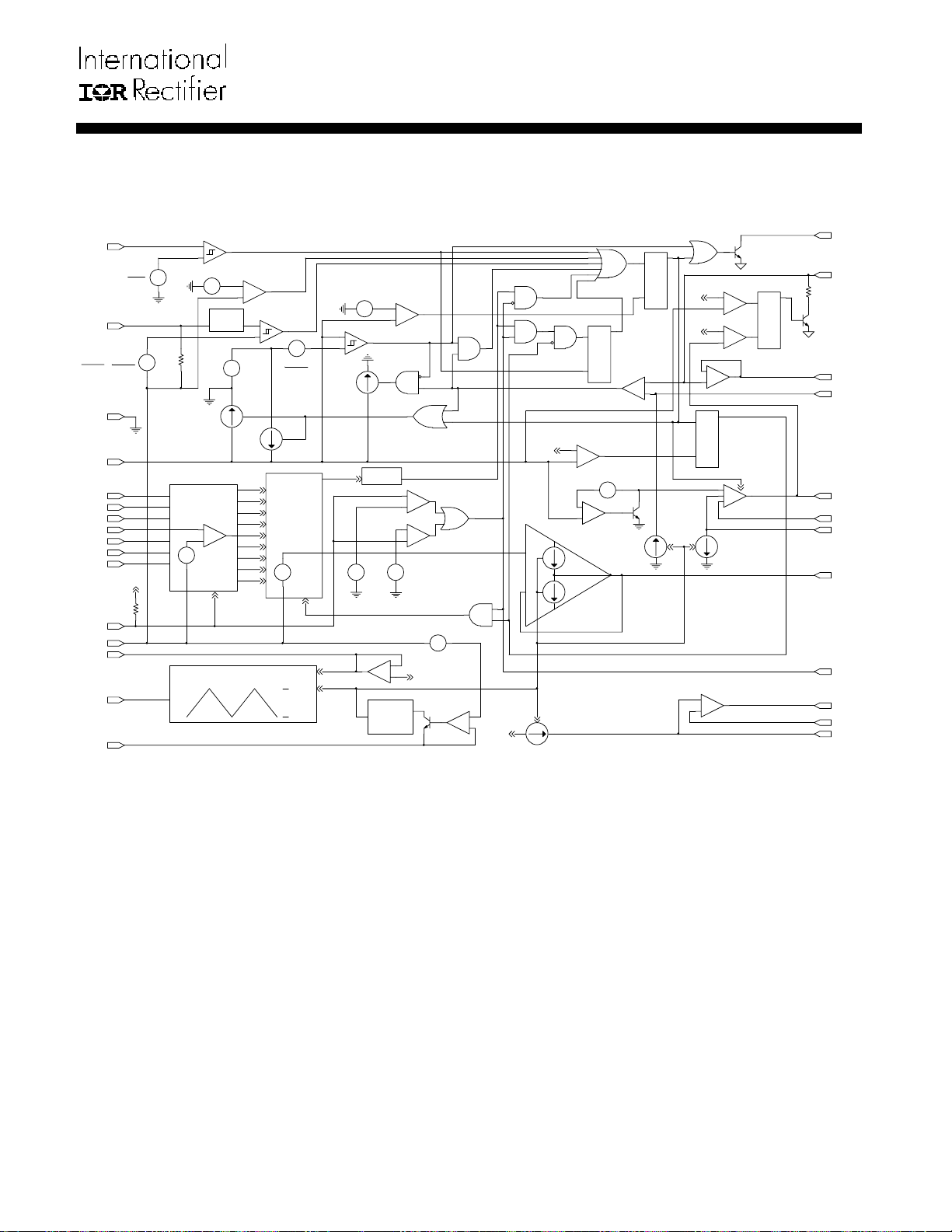
IR3084U THEORY OF OPERATION
Block Diagram
VCC UVLO
100k
VID INPUT
COMPARATORS
(1 OF 9
SHOWN)
+
-
50%
DUTY
CYCLE
COMPARATOR
-
+
2.0V
-
250ns
BLANKING
IHICCUP
DISCHARGE
6.5uA
+
-
INTEL: 0.6V
AMD: 1.24V
INTEL/AMD
RAMP GENERATOR
+
+
-
VOSNS FLOAT
DETECT
-
+
ENABLE
COMPARATOR
-
+
VCHG
3.85V
ON
ICHG
70uA
DIGITAL TO
IROSC
ANALOG
IROSC
CONVERTER
IROSC
IROSC
IROSC
IROSC
IROSC
IROSC
IROSC
+
80mV
100mV
OFF
"FAST"
VDAC
+
-
1.1V
4.8V
0.9V
-
0.215V
-
-
+
OC
DISCHARGE
CURRENT
40uA
IROSC
+
-
VBIAS
IROSC
DISCHARGE
+
COMPARATOR
+
-
DELAY
COMPARATOR
ON
SS/DEL
DISCHARGE
1.3us
BLANKING
+
1.95V0.6V
-
VID = 1.1V BOOT
-
6.9V
+
CURRENT
SOURCE
GENERATOR
-
+
-
+
-
VBIAS
REGULATOR
NO_CPU
1.2V
ROSC
BUFFER
AMP
UVLO
VOSNS OPEN
DISABLE
OVER CURRENT
NO CPU
NO CPU LATCHED
S
SET
R
OC
COMPARATOR
VID SAMPLE
DELAY COMPARATOR
-
3.1V
+
1.3V
-
ISOURCE
ISINK
VDAC
BUFFER
AMP
IREGSET
+
-
SOFTSTART
CLAMP
INTL_MD
+
-
+
+
-
VCC
IROSC
DOMINANT
VID
FAULT
LATCH
+
IOCSET
S
R
FAULT
LATCH
+
-
IROSC
SET
DOMINANT
0.6V
+
S
-
0.35V
-
R
+
VDRP
-
AMP
+
S
START
LATCH
SET
DOMINANT
R
DISABLE
+
+
-
ERROR
AMP
INTEL: IOFFSET
IROSC
AMD: -IOFFSET
BIAS
REGULATOR
+
ERROR AMP
-
VCC
ENABLE
850mV
750mV
LGND
SS/DEL
VID6
VID5
VID4
VID3
VID2
VID1
VID0
VIDSEL
VOSNS-
VBIAS
RMPOUT
ROSC
AMDINTEL
1.23V
1.17V
4.5K
9.9V
9.1V
2.4V
+
-
+
-
Figure 7 – IR3084U Block Diagram
VID Control
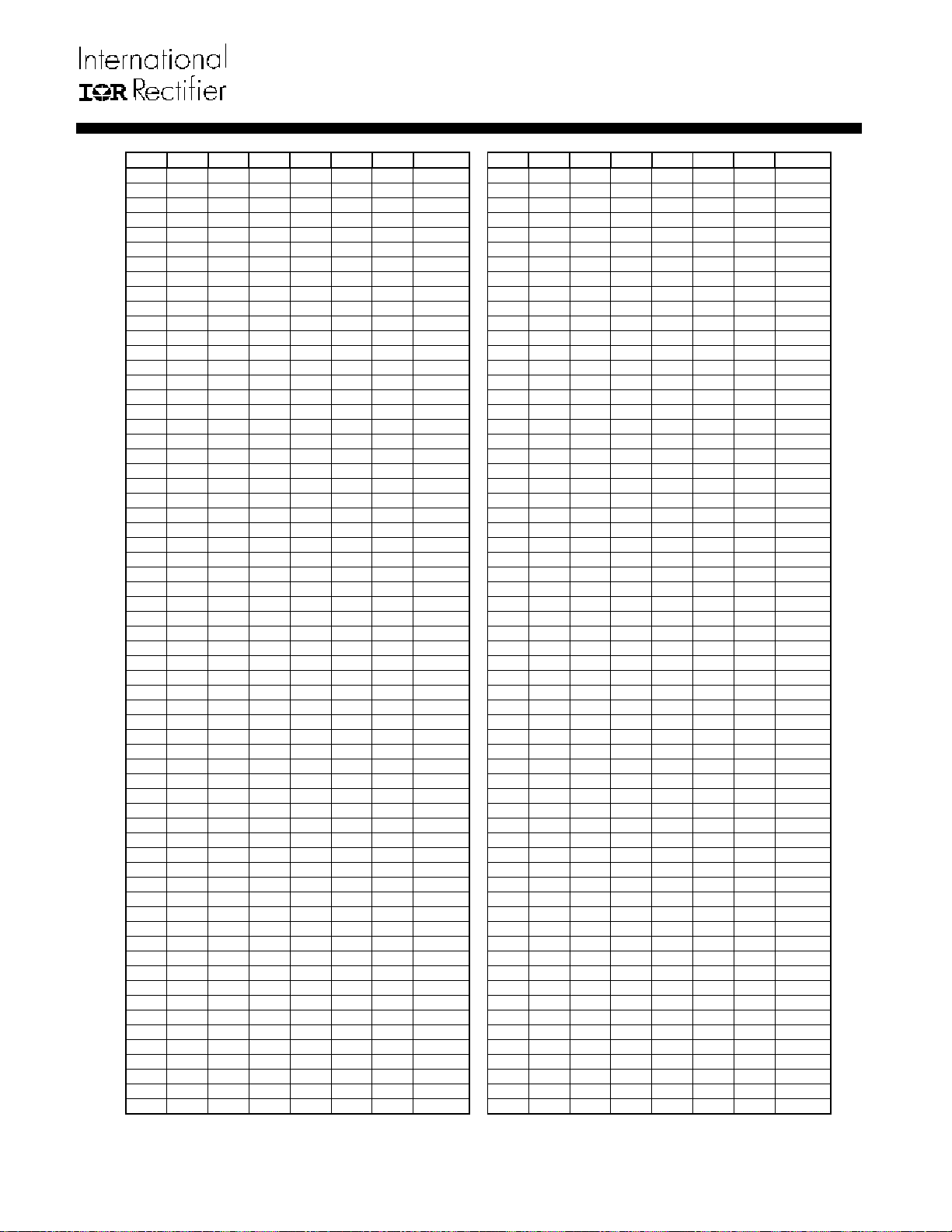
A 7-bit VID voltage compatible with VR10 (see Table 1) and VR11 (see Table 2) and Opteron/Athlon64 (see
Table 3) is available at the VDAC pin. The VIDSEL pin configures the DAC for VR10 if grounded, VR11 if
floating, and Opteron/Athlon64 if connected to GND via a 6.4K resistor. The VIDSEL pin is internally pulled-up to
2.4V through a 4.5Kohm resistor. The VID pins require an external bias voltage and should not be floated. The
VID input comparators, with 0.6V reference for VR10/VR11 and 1.24V for Opteron/Athlon64, monitor the VID
pins and control the 7-bit Digital-to-Analog Converter (DAC) whose output is sent to the VDAC buffer amplifier.
The output of the buffer amp is the VDAC pin. The VDAC voltage is post-package trimmed to compensate for
the input offsets of the Error Amp to provide a 0.5% system accuracy. The actual VDAC voltage does not
represent the system set point and has a wider tolerance.
SET
DOMINANT
IIN
PRECONDITIONING
LATCH
VRRDY
IIN
12.5K
VDRP
OCSET
EAOUT
FB
VSETPT
VDAC
INTL_MD
REGDRV
REGFB
REGSE T
Page 14 of 47 9/14/2005
IR3084U
VID4 VID3 VID2 VID1 VID0 VID5 VID6 Voltage VID4 VID3 VID2 VID1 VID0 VID5 VID6 Voltage
0 1 0 1 0 1 1 1.60000 1 1 0 1 0 1 1 1.20000
0 1 0 1 0 1 0 1.59375 1 1 0 1 0 1 0 1.19375
0 1 0 1 1 0 1 1.58750 1 1 0 1 1 0 1 1.18750
0 1 0 1 1 0 0 1.58125 1 1 0 1 1 0 0 1.18125
0 1 0 1 1 1 1 1.57500 1 1 0 1 1 1 1 1.17500
0 1 0 1 1 1 0 1.56875 1 1 0 1 1 1 0 1.16875
0 1 1 0 0 0 1 1.56250 1 1 1 0 0 0 1 1.16250
0 1 1 0 0 0 0 1.55625 1 1 1 0 0 0 0 1.15625
0 1 1 0 0 1 1 1.55000 1 1 1 0 0 1 1 1.15000
0 1 1 0 0 1 0 1.54375 1 1 1 0 0 1 0 1.14375
0 1 1 0 1 0 1 1.53750 1 1 1 0 1 0 1 1.13750
0 1 1 0 1 0 0 1.53125 1 1 1 0 1 0 0 1.13125
0 1 1 0 1 1 1 1.52500 1 1 1 0 1 1 1 1.12500
0 1 1 0 1 1 0 1.51875 1 1 1 0 1 1 0 1.11875
0 1 1 1 0 0 1 1.51250 1 1 1 1 0 0 1 1.11250
0 1 1 1 0 0 0 1.50625 1 1 1 1 0 0 0 1.10625
0 1 1 1 0 1 1 1.50000 1 1 1 1 0 1 1 1.10000
0 1 1 1 0 1 0 1.49375 1 1 1 1 0 1 0 1.09375
0 1 1 1 1 0 1 1.48750 1 1 1 1 1 0 1 FAULT
0 1 1 1 1 0 0 1.48125 1 1 1 1 1 0 0 FAULT
0 1 1 1 1 1 1 1.47500 1 1 1 1 1 1 1 FAULT
0 1 1 1 1 1 0 1.46875 1 1 1 1 1 1 0 FAULT
1 0 0 0 0 0 1 1.46250 0 0 0 0 0 0 1 1.08750
1 0 0 0 0 0 0 1.45625 0 0 0 0 0 0 0 1.08125
1 0 0 0 0 1 1 1.45000 0 0 0 0 0 1 1 1.07500
1 0 0 0 0 1 0 1.44375 0 0 0 0 0 1 0 1.06875
1 0 0 0 1 0 1 1.43750 0 0 0 0 1 0 1 1.06250
1 0 0 0 1 0 0 1.43125 0 0 0 0 1 0 0 1.05625
1 0 0 0 1 1 1 1.42500 0 0 0 0 1 1 1 1.05000
1 0 0 0 1 1 0 1.41875 0 0 0 0 1 1 0 1.04375
1 0 0 1 0 0 1 1.41250 0 0 0 1 0 0 1 1.03750
1 0 0 1 0 0 0 1.40625 0 0 0 1 0 0 0 1.03125
1 0 0 1 0 1 1 1.40000 0 0 0 1 0 1 1 1.02500
1 0 0 1 0 1 0 1.39375 0 0 0 1 0 1 0 1.01875
1 0 0 1 1 0 1 1.38750 0 0 0 1 1 0 1 1.01250
1 0 0 1 1 0 0 1.38125 0 0 0 1 1 0 0 1.00625
1 0 0 1 1 1 1 1.37500 0 0 0 1 1 1 1 1.00000
1 0 0 1 1 1 0 1.36875 0 0 0 1 1 1 0 0.99375
1 0 1 0 0 0 1 1.36250 0 0 1 0 0 0 1 0.98750
1 0 1 0 0 0 0 1.35625 0 0 1 0 0 0 0 0.98125
1 0 1 0 0 1 1 1.35000 0 0 1 0 0 1 1 0.97500
1 0 1 0 0 1 0 1.34375 0 0 1 0 0 1 0 0.96875
1 0 1 0 1 0 1 1.33750 0 0 1 0 1 0 1 0.96250
1 0 1 0 1 0 0 1.33125 0 0 1 0 1 0 0 0.95625
1 0 1 0 1 1 1 1.32500 0 0 1 0 1 1 1 0.95000
1 0 1 0 1 1 0 1.31875 0 0 1 0 1 1 0 0.94375
1 0 1 1 0 0 1 1.31250 0 0 1 1 0 0 1 0.93750
1 0 1 1 0 0 0 1.30625 0 0 1 1 0 0 0 0.93125
1 0 1 1 0 1 1 1.30000 0 0 1 1 0 1 1 0.92500
1 0 1 1 0 1 0 1.29375 0 0 1 1 0 1 0 0.91875
1 0 1 1 1 0 1 1.28750 0 0 1 1 1 0 1 0.91250
1 0 1 1 1 0 0 1.28125 0 0 1 1 1 0 0 0.90625
1 0 1 1 1 1 1 1.27500 0 0 1 1 1 1 1 0.90000
1 0 1 1 1 1 0 1.26875 0 0 1 1 1 1 0 0.89375
1 1 0 0 0 0 1 1.26250 0 1 0 0 0 0 1 0.88750
1 1 0 0 0 0 0 1.25625 0 1 0 0 0 0 0 0.88125
1 1 0 0 0 1 1 1.25000 0 1 0 0 0 1 1 0.87500
1 1 0 0 0 1 0 1.24375 0 1 0 0 0 1 0 0.86875
1 1 0 0 1 0 1 1.23750 0 1 0 0 1 0 1 0.86250
1 1 0 0 1 0 0 1.23125 0 1 0 0 1 0 0 0.85625
1 1 0 0 1 1 1 1.22500 0 1 0 0 1 1 1 0.85000
1 1 0 0 1 1 0 1.21875 0 1 0 0 1 1 0 0.84375
1 1 0 1 0 0 1 1.21250 0 1 0 1 0 0 1 0.83750
1 1 0 1 0 0 0 1.20625 0 1 0 1 0 0 0 0.83125
Table 1 – VR10 7-bit VID Table with 6.25mV Extension
Page 15 of 47 9/14/2005
 Loading...