International Rectifier IR2153, IR2153S Datasheet

Data Sheet No. PD-6.062A
Next Data SheetIndex
Previous Datasheet
To Order
IR2153
SELF-OSCILLATING HALF-BRIDGE DRIVER
Features
n Floating channel designed for bootstrap operation
Fully operational to +600V
Tolerant to negative transient voltage
dV/dt immune
n Undervoltage lockout
n Programmable oscillator frequency
f =
1.4 (R 75 ) C
nMatched propagation delay for both channels
n Micropower supply startup current of 90 µA.
n Shutdown function turns off both channels
n Low side output in phase with R
1
×+ ×
Ω
TT
T
Description
The IR2153 is a high voltage, high speed, self-oscillating power MOSFET and IGBT driver with both high
and low side referenced output channels. Proprietary
HVIC and latch immune CMOS technologies enable
ruggedized monolithic construction. The front end features a programmable oscillator which is similar to the
555 timer. The output drivers feature a high pulse current buff er stage and an internal deadtime designed f or
minimum driver cross-conduction. Propagation dela ys
for the two channels are matched to simplify use in
50% duty cycle applications. The floating channel can
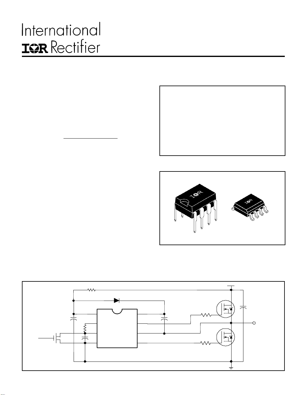
Typical Connection
Product Summary
V
OFFSET
Duty Cycle 50%
IO+/- 200 mA / 400 mA
V
clamp
Deadtime (typ.) 1.2 µs
600V max.
15.6V
Packages
be used to drive an N-channel power MOSFET or
IGBT in the high side configuration that operates off
a high voltage rail up to 600 volts.
up to 600V
V
CC
R
T
T
M
V
B
H
V
S
L
TO
LOAD
1
1/6/97

IR2153
Next Data SheetIndex
Previous Datasheet
To Order
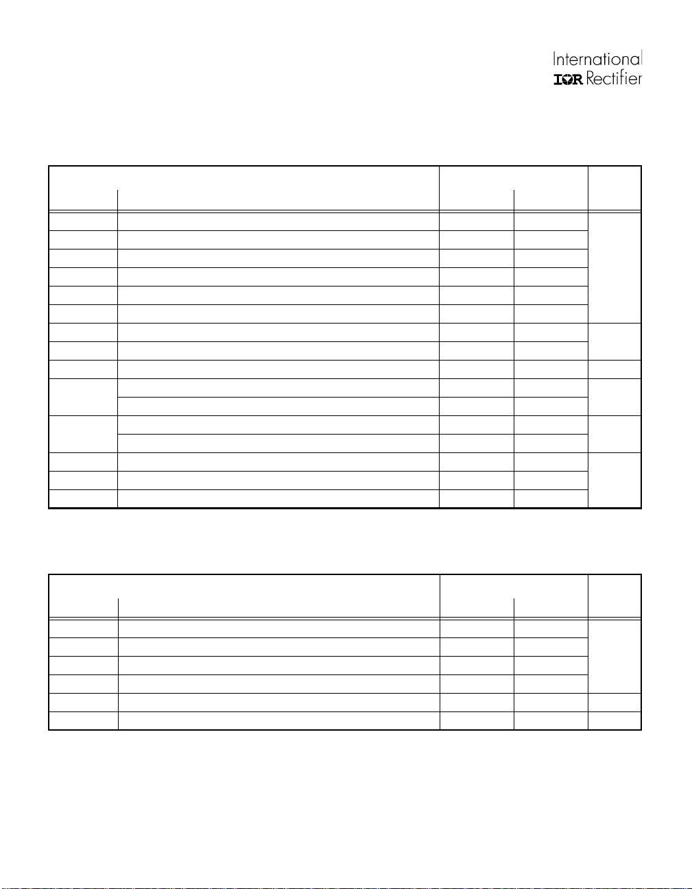
Absolute Maximum Ratings
Absolute Maximum Ratings indicate sustained limits beyond which damage to the device may occur. All voltage parameters are absolute voltages referenced to COM. The Thermal Resistance and Power Dissipation ratings are measured
under board mounted and still air conditions.
Parameter Value
Symbol Definition Min. Max. Units
V
B
V
S
V
HO
V
LO
V
RT
V
CT
I
CC
I
RT
dVs/dt Allowable Offset Supply Voltage Transient — 50 V/ns
P
D
R
θJA
T
J
T
S
T
L
High Side Floating Supply Voltage -0.3 625
High Side Floating Supply Offset Voltage VB - 25 VB + 0.3
High Side Floating Output Voltage VS - 0.3 V
Low Side Output Voltage -0.3 VCC + 0.3
RT V oltage -0.3 VCC + 0.3
CT Voltage -0.3 V
Supply Current (Note 1) — 25
RT Output Current -5 5
Package Power Dissipation @ TA ≤ +25°C (8 Lead DIP) — 1.0
(8 Lead SOIC) — 0.625
Thermal Resistance, Junction to Ambient (8 Lead DIP) — 125
(8 Lead SOIC) — 200
Junction Temperature — 150
Storage Temperature -55 150 °C
Lead Temperature (Soldering, 10 seconds) — 300
CC
B
+ 0.3
+ 0.3
mA
°C/W
V
W
Recommended Operating Conditions
The Input/Output logic timing diagram is shown in Figure 1. For proper operation the device should be used within the
recommended conditions. The V
Symbol Definition Min. Max. Units
V
B
V
S
V
HO
V
LO
I
CC
T
A
Note 1: Because of the IR2153’s application specificity toward off-line supply systems, this IC contains a zener clamp
2
High Side Floating Supply Absolute Voltage VS + 10 VS + 20
High Side Floating Supply Offset Voltage — 600
High Side Floating Output Voltage V
Low Side Output Voltage 0 V
Supply Current (Note 1) — 5 mA
Ambient Temperature -40 125 °C
structure between the chip VCC and COM which has a nominal breakdown voltage of 15.6V. Theref or e, the IC
supply voltage is normally derived by forcing current into the supply lead (typically by means of a high value
resistor connected between the chip V
to COM) and allowing the internal zener clamp circuit to deter mine the nominal supply voltage. There-
V
CC
fore, this circuit should not be driven by a DC, low impedance power source of greater than V
offset rating is tested with all supplies biased at 15V differential.
S
Parameter Value
S
and the rectified line voltage and a local decoupling capacitor from
CC
V
B
CC
CLAMP
V
.

IR2153
Next Data SheetIndex
Previous Datasheet
To Order
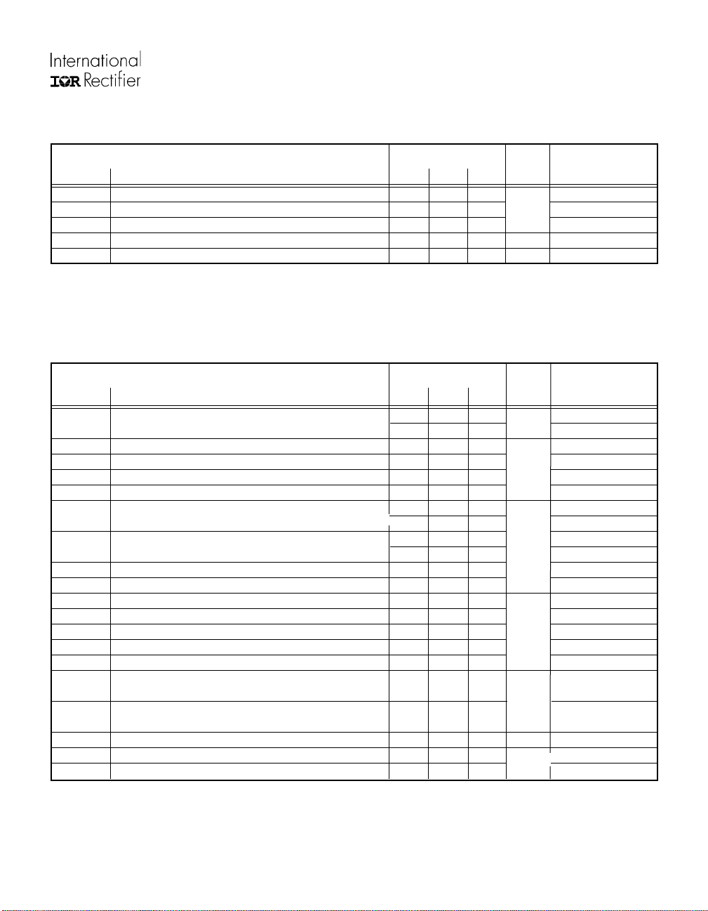
Dynamic Electrical Characteristics
V
(VCC, VBS) = 12V, CL = 1000 pF and TA = 25°C unless otherwise specified.
BIAS
Parameter Value
Symbol Definition Min. Typ. Max. Units Test Conditions
t
t
t
sd
DT Deadtime
DR
Turn-On Rise Time — 80
r
Turn-Off Fall Time — 35
f
Shutdown Propagation Delay
—
—
Duty Cycle
T
—
Static Electrical Characteristics
V
(VCC, VBS) = 12V, CL = 1000 pF, CT = 1 nF and TA = 25°C unless otherwise specified. The VIN, VTH and I
BIAS
parameters are referenced to COM. The VO and IO parameters are referenced to COM and are applicable to the
respective output leads: HO or LO.
Parameter Value
Symbol Definition Min. Typ. Max. Units Test Conditions
f
OSC
V
CLAMP
V
V
V
CTSD
V
V
V
V
I
I
QBS
I
QCCUV
I
QCC
I
V
CCUV+
V
CCUV-
V
CCUVH
I
I
CT+
CT-
RT+
RT-
OH
OL
LK
CT
O+
O-
Oscillator Frequency — 20.0 — RT = 35.7 kΩ
— 100 — RT = 7.04 kΩ
VCC Zener Shunt Clamp Voltage — 15.6 — ICC = 5 mA
2/3 VCC Threshold — 8.0 —
1/3 VCC Threshold — 4.0 —
CT shutdown Input Threshold — 2.2 —
RT High Level Output Voltage, VCC - R
T
— 0 100 IRT = -100 µA
— 200 300 IRT = -1 mA
RT Low Level Output Voltage — 20 50 IRT = 100 µ A
— 200 300 IRT = 1 mA
High Level Output Voltage, V
Low Level Output V oltage, V
BIAS
O
- V
O
— — 100 IO = 0A
— — 100 IO = 0A
Offset Supply Leakage Current — — 50 VB = VS = 600V
Quiescent VBS Supply Current — 10 —
Micropower VCC Supply Startup Current — 90 — µA V
Quiescent VCC Supply Current — 400 — V
CT Input Current — 0.001 1.0
VCC Supply Undervoltage Positive Going — 9.0 —
Threshold
VCC Supply Undervoltage Negative Going — 8.0 —
Threshold
VCC Supply Undervoltage Lockout Hysteresis — 1.0 — V
Output High Short Circuit Pulsed Current — 200 — VO = 0V
Output Low Short Circuit Pulsed Current — 400 — VO = 15V
—
—
—
660
—
1.2
50 — %
ns
µs
kHz
V
mV
V
mA
CC
CC
< V
> V
IN
CCUV
CCUV
3
 Loading...