International Rectifier IR2128S, IR2128 Datasheet

Data Sheet No. PD-6.042D
Next Data SheetIndex
Previous Datasheet
To Order
IR2128
CURRENT SENSING SINGLE CHANNEL DRIVER
Features
n Floating channel designed for bootstrap operation
Fully operational to +600V
Tolerant to negative transient voltage
dV/dt immune
n Gate drive supply range from 10 to 20V
n Undervoltage lockout
n 5V Schmitt-triggered input logic
FAULT
n
n Output out of phase with input
lead indicates shutdown has occured
Description
The IR2128 is a high voltage, high speed power
MOSFET and IGBT driver. Proprietar y HVIC and
latch immune CMOS technologies enable ruggedized monolithic construction. The logic input is
compatible with standard CMOS or LSTTL outputs.
The protection circuity detects over-current in the
driven power transistor and terminates the gate
FAULT
drive voltage. An open drain
vided to indicate that an over-current shutdown has
occurred. The output driver features a high pulse
current buffer stage designed for minimum crossconduction. The floating channel can be used to
drive an N-channel power MOSFET or IGBT in the
high side or low side configuration which operates
up to 600 volts.
signal is pro-
Product Summary
V
OFFSET
IO+/- 200 mA / 420 mA
V
OUT
V
CSth
t
(typ.) 150 & 100 ns
on/off
Packages
600V max.
10 - 20V
250 mV
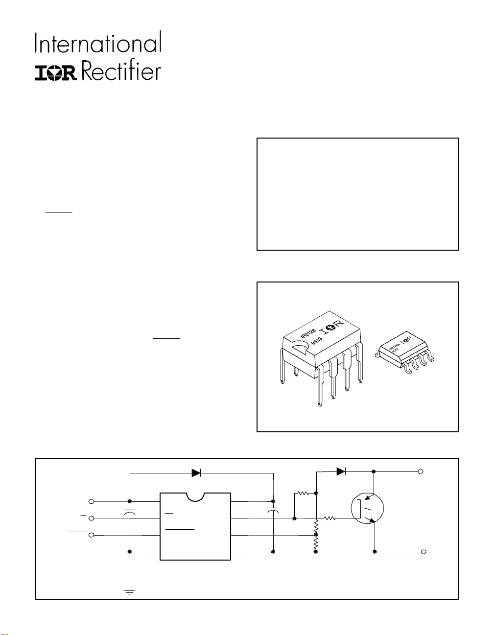
Typical Connection
V
CC
IN
FAULT
V
CC
IN
FAULT
COM
V
B
HO
CS
V
S
CONTROL INTEGRATED CIRCUIT DESIGNERS MANUAL B-129

IR2128
Next Data SheetIndex
Previous Datasheet
To Order
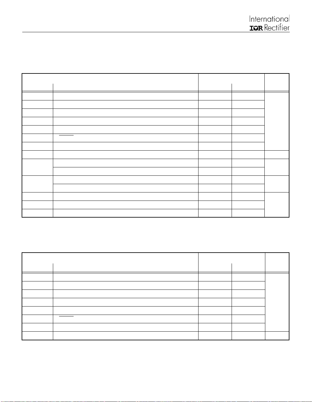
Absolute Maximum Ratings
Absolute Maximum Ratings indicate sustained limits beyond which damage to the device may occur. All voltage parameters are absolute voltages referenced to COM. The Ther mal Resistance and Power Dissipation ratings are measured
under board mounted and still air conditions.
Parameter Value
Symbol Definition Min. Max. Units
V
B
V
S
V
HO
V
CC
V
IN
V
FLT
V
CS
dVs/dt Allowable Offset Supply Voltage Transient — 50 V/ns
P
D
R
θJA
T
J
T
S
T
L
High Side Floating Supply Voltage -0.3 625
High Side Floating Offset Voltage VB - 25 VB + 0.3
High Side Floating Output Voltage VS - 0.3 V
B
+ 0.3
Logic Supply Voltage -0.3 25 V
Logic Input Voltage -0.3 V
Output Voltage -0.3 V
FAULT
Current Sense Voltage VS - 0.3 V
Package Power Dissipation @ TA ≤ +25°C (8 Lead DIP) — 1.0
(8 Lead SOIC) — 0.625
Thermal Resistance, Junction to Ambient (8 Lead DIP) — 125
(8 Lead SOIC) — 200
CC
CC
B
+ 0.3
+ 0.3
+ 0.3
W
°C/W
Junction Temperature — 150
Storage Temperature -55 150 °C
Lead Temperature (Soldering, 10 seconds) — 300
Recommended Operating Conditions
The Input/Output logic timing diagram is shown in Figure 1. For proper operation the device should be used within the
recommended conditions. The VS offset rating is tested with all supplies biased at 15V differential.
Parameter Value
Symbol Definition Min. Max. Units
V
B
V
S
V
HO
V
CC
V
IN
V
FLT
V
CS
T
A
Note 1: Logic operational for VS of -5 to +600V. Logic state held for VS of -5V to -VBS.
B-130 CONTROL INTEGRATED CIRCUIT DESIGNERS MANUAL
High Side Floating Supply Voltage VS + 10 VS + 20
High Side Floating Offset Voltage Note 1 600
High Side Floating Output Voltage V
S
Logic Supply Voltage 11.8 20 V
Logic Input Voltage 0 V
Output Voltage 0 V
FAULT
Current Sense Signal Voltage V
S
V
Ambient Temperature -40 125 °C
V
B
CC
CC
+ 5
S
 Loading...