

INTERNATIONAL RECTIFIER IR 2011S Datasheet
Data Sheet No.PD60217 revB
IR2011(
HIGH AND LOW SIDE DRIVER
Features
· Floating channel designed for bootstrap operation
Fully operational up to +200V
Tolerant to negative transient voltage, dV/dt immune
· Gate drive supply range from 10V to 20V
· Independent low and high side channels
· Input logicHIN/LIN active high
· Undervoltage lockout for both channels
· 3.3V and 5V input logic compatible
· CMOS Schmitt-triggered inputs with pull-down
· Matched propagation delay for both channels
· Also available LEAD-FREE (PbF)
Applications
· Audio Class D amplifiers
· High power DC-DC SMPS converters
· Other high frequency applications
Description
The IR2011 is a high power, high speed power MOSFET driver with independent high
and low side referenced output channels, ideal for Audio Class D and DC-DC converter
applications. Logic inputs are compatible with standard CMOS or LSTTL output, down
to 3.0V logic. The output drivers feature a high pulse current buffer stage designed for
minimum driver cross-conduction. Propagation delays are matched to simplify use in
high frequency applications. The floating channel can be used to drive an N-channel
power MOSFET in the high side configuration which operates up to 200 volts. Proprietary HVIC and latch immune CMOS technologies enable ruggedized monolithic construction.
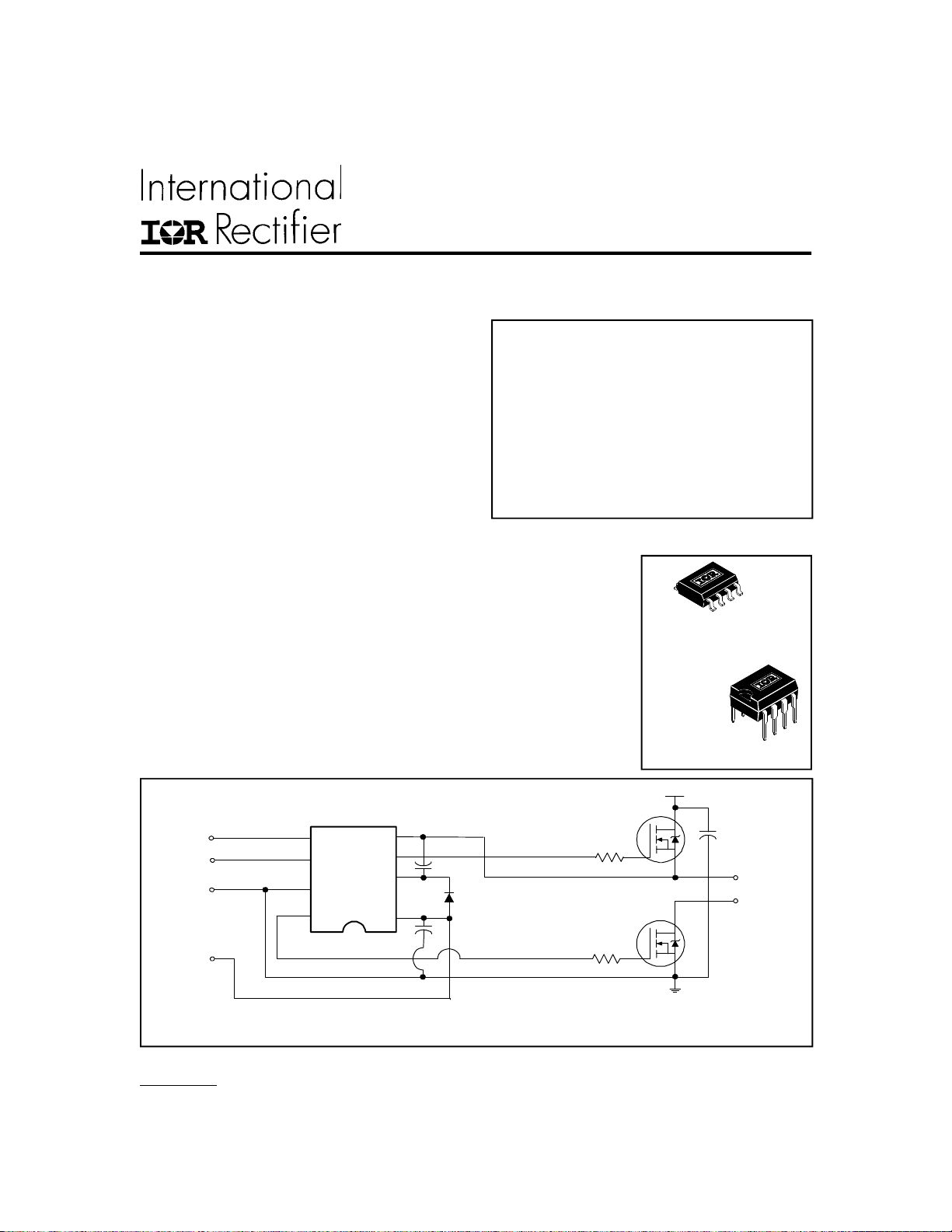
Typical Connection
Product Summary
V
OFFSET
IO+/- 1.0A /1.0A typ.
V
OUT
t
on/off
Delay Matching 20 ns max.
S) & (PbF
200V max.
10 - 20V
80 & 60 ns typ.
Packages
8-Lead SOIC
IR2011S
8-Lead PDIP
IR2011
200V
)
45
V
V
HO
V
CC
S
B
18
TO
LOAD
HIN
LIN
COM
V
CC
(Refer to Lead Assignments for correct configuration). This/These diagram(s) show electrical connections only. Please
refer to our Application Notes and DesignTips for proper circuit board layout.
www.irf.com 1
HIN
LIN
COM
LO

IR2011(S) & (PbF)
Absolute Maximum Ratings
Absolute maximum ratings indicate sustained limits beyond which damage to the device may occur. All voltage parameters are absolute voltages referenced to COM. The thermal resistance and power dissipation ratings are measured
under board mounted and still air conditions.
Symbol Definition Min. Max. Units
V
B
V
S
V
HO
V
CC
V
LO
V
IN
dVs/dt Allowable offset supply voltage transient (figure 2) — 50 V/ns
P
D
R
THJA
T
J
T
S
T
L
High side floating supply voltage -0.3 225
High side floating supply offset voltage VB - 25 VB + 0.3
High side floating output voltage VS - 0.3 V
Low side fixed supply voltage -0.3 25
Low side output voltage -0.3 VCC +0.3
Logic input voltage (HIN & LIN) -0.3 V
Package power dissipation @ T
Thermal resistance, junction to ambient (8-lead DIP) — 125
Junction temperature — 150
Storage temperature -55 150
Lead temperature (soldering, 10 seconds) — 300
£ +25°C (8-lead DIP) — 1.0
A
(8-lead SOIC) — 0.625
(8-lead SOIC) — 200
B
CC
+ 0.3
+0.3
°C/W
V
W
°C
Recommended Operating Conditions
For proper operation the device should be used within the recommended conditions. The VS and COM offset ratings
are tested with all supplies biased at 15V differential.
Symbol Definition Min. Max. Units
V
B
V
S
V
HO
V
CC
V
LO
V
IN
T
A
Note 1: Logic operational for VS of -4 to +200V. Logic state held for VS of -4V to -VBS.
2 www.irf.com
High side floating supply absolute voltage VS + 10 VS + 20
High side floating supply offset voltage Note 1 200
High side floating output voltage V
Low side fixed supply voltage 10 20
Low side output voltage 0 VCC
Logic input voltage (HIN & LIN) COM 5.5
Ambient temperature -40 125 °C
S
V
B
V
IR2011(S) & (PbF)
Dynamic Electrical Characteristics
V
(VCC, VBS) = 15V, CL = 1000 pF, T
BIAS
Symbol Definition Min. Typ.Max.UnitsTest Conditions
t
on
t
off
DM1 Turn-on delay matching | t
DM2 Turn-off delay matching | t
Turn-on propagation delay — 80 — VS = 0V
Turn-off propagation delay — 75 — VS = 200V
t
Turn-on rise time — 35 50
r
t
Turn-off fall time — 20 35
f
Static Electrical Characteristics
V
(VCC, VBS) = 15V, and T
BIAS
COM and are applicable to all logic input leads: HIN and LIN. The VO and IO parameters are referenced to COM and are
applicable to the respective output leads: HO or LO.
= 25°C unless otherwise specified. The V
A
= 25°C unless otherwise specified. Figure 1 shows the timing definitions.
A
ns
(H) - t
on
(H) - t
off
(L) | — — 20
on
(L) | — — 20
off
, VTH and IIN parameters are referenced to
IN
Symbol Definition Min. Typ.Max.UnitsTest Conditions
V
IH
V
V
OH
V
OL
I
LK
I
QBS
I
QCC
I
IN+
I
IN-
V
BSUV+
V
BSUV-
V
CCUV+
V
CCUV-
I
O+
I
O-
www.irf.com 3
Logic “1” input voltage 2.2 — —
Logic “0” input voltage — — 0.7
IL
High level output voltage, V
Low level output voltage, V
BIAS
O
- V
O
— — 2.0 IO = 0A
— — 0.2 20mA
V
Offset supply leakage current — — 50 VB=VS = 200V
Quiescent VBS supply current — 90 210 V
Quiescent VCC supply current — 140 230 VIN = 0V or 3.3V
µA
Logic “1” input bias current — 7.0 20 VIN = 3.3V
Logic “0” input bias current — — 1.0 V
VBS supply undervoltage positive going 8.2 9.0 9.8
threshold
VBS supply undervoltage negative going 7.4 8.2 9.0
threshold
V
VCC supply undervoltage positive going 8.2 9.0 9.8
threshold
VCC supply undervoltage negative going 7.4 8.2 9.0
threshold
Output high short circuit pulsed current — 1.0 — VO = 0V,
Output low short circuit pulsed current — 1.0 — VO = 15V,
A
VCC = 10V - 20V
= 0V or 3.3V
IN
= 0V
IN
PW £ 10 µs
PW £ 10 µs
IR2011(S) & (PbF)
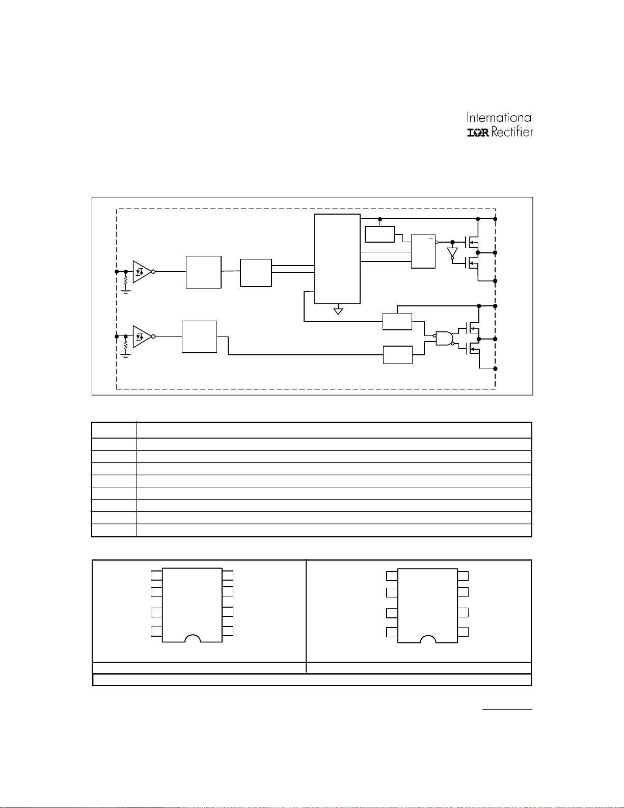
Functional Block Diagram
HIGH
VOLTAGE
3V S-TRIGGER
HIN
3V S-TRIGGER
LIN
LOW
VOLTAGE
LEVEL
SHIFT
LOW
VOLTAGE
LEVEL
SHIFT
BUFFER
Lead Definitions
SymbolDescription
HIN Logic input for high side gate driver output (HO), in phase
LIN Logic input for low side gate driver output (LO), in phase
V
B
HO High side gate drive output
V
S
V
CC
LO Low side gate drive output
COM Low side return
High side floating supply
High side floating supply return
Low side supply
LEVEL
SHIFT
CIRCUIT
UV
DETECT
DETECT
UV
DELAY
UV Q
S
R
V
B
HO
V
S
V
CC
LO
COM
Lead Assignments
V
V
HO
V
CC
4
S
3
2
B
1
5
6
7
8
HIN
LIN
COM
LO
5
6
7
8
HIN
LIN
COM
LO
8-Lead PDIP 8-Lead SOIC
IR2011 IR2011S
Part Number
4 www.irf.com
V
V
HO
V
CC
4
S
3
2
B
1
IR2011(S) & (PbF)
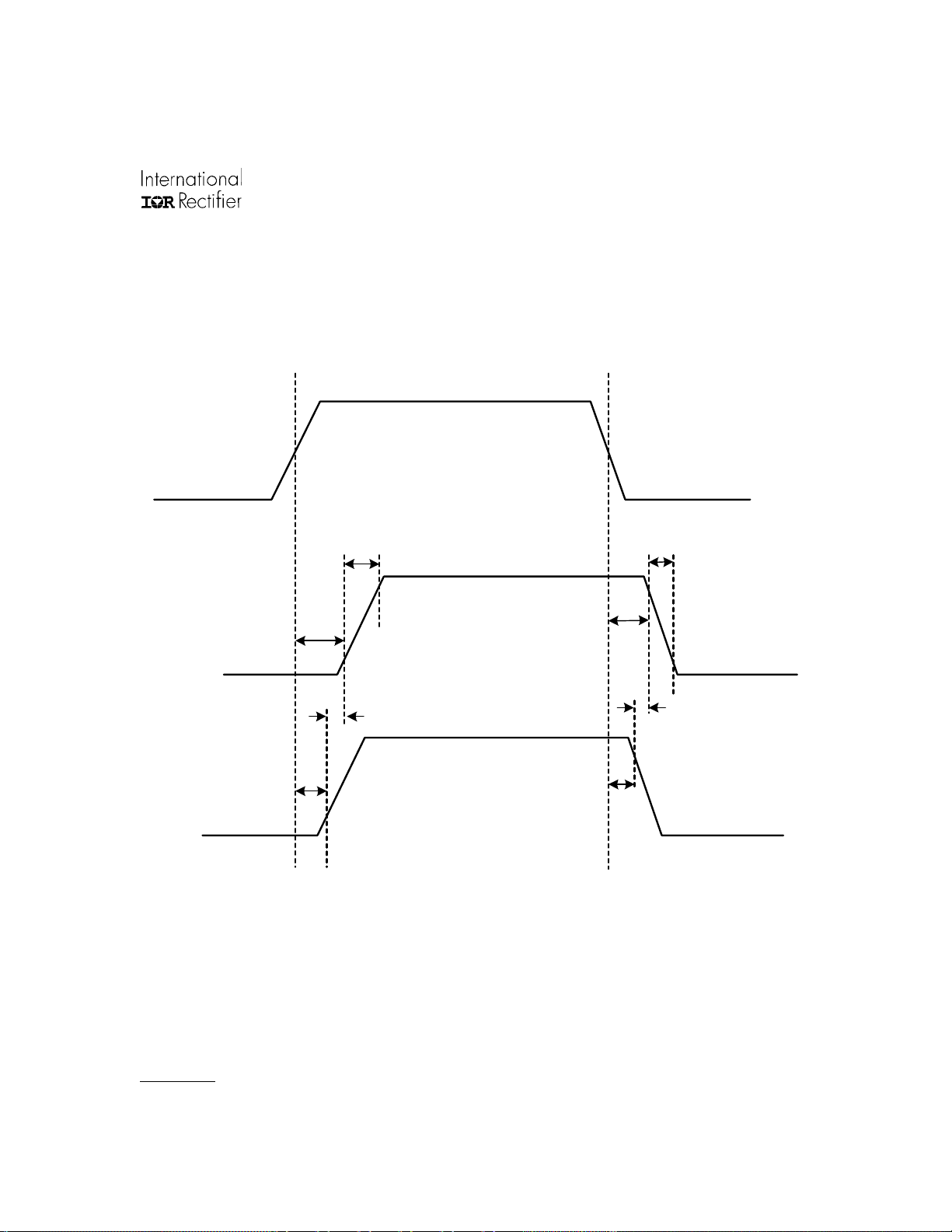
50%
ton(L)
ton(H)
10%
10%
t
rise
DM1
90%
50%
HIN / LIN
t
fall
90%
t
(H)
off
t
(L)
off
10%
DM2
90%
HO
LO
Figure 1. Timing Diagram
www.irf.com 5
IR2011(S) & (PbF)
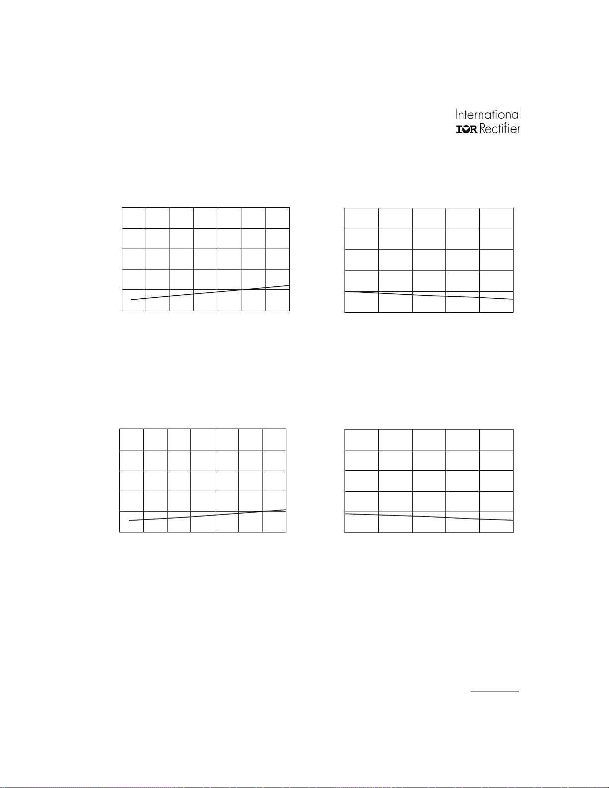
Turn-on Propagation Delay (ns)
Tu rn -on P ro pag ation De lay ( ns )
Typ.
500
400
300
200
100
Typ.
0
-50 -25 0 25 50 75 100 125
Temperature (oC)
Figure 2A. Turn-on Propagation Delay
vs. Temperature
500
400
300
200
500
400
300
200
Typ.
100
0
10 12 14 16 18 20
Supply Voltage (V)
Figure 2B. Turn-on Propagation Delay
vs. Supply Voltage
500
400
300
200
100
Typ.
0
Turn-off Propagation Delay (ns)
-50 -25 0 25 50 75 100 125
Temperature (oC)
Figure 3A. Turn-off Propagation Delay
vs. Temperature
100
0
Turn- off Propagation Delay (ns)
10 12 14 16 18 20
Supply Voltage (V)
Figure 3B. Turn-off Propagation Delay
vs. Supply Voltage
6 www.irf.com
 Loading...