International Rectifier IP2005ATRPBF, IP2005A Datasheet
PD-60325
iP2005APbF
High Frequency Synchronous Buck
Optimized LGA Power Stage
Integrated Power Semiconductors, Driver IC, & Passives
Features
• 40A Multiphase building block
• No de-rating up to T
PCB
= 95ºC
• Optimized for low power loss
• Optimized for low EMI
• Bias supply range of 4.5V to 7.0V
• Operation up to 1.5MHz
• Bi-directional Current flow
• Under Voltage Lockout
• LGA interface
• 7.65mm x 7.65mm outline
Description
The iP2005A is a fully optimized solution for high curr ent
synchronous buck multiphase applications. Board space
and design time are greatly reduced because most of
the components required for each phase of a typical
discrete-based multiphase circuit are integrated into a
single 7.65mm x 7.65mm x 1.66mm power block. The
additional components required for a complete
multiphase converter are a PWM controller, the output
inductors, and the input and output capacitors.
iPOWIR Technology offers designers an innovative
board space saving solution for applications requiring
high power densities. iPOWIR technology eases design
for applications where component integration offers
benefits in performance and functionality. iPOWIR
technology solutions are also optimized internally for
layout, heat transfer, and component selection.
Applications
• High Frequency, Low Profile DC-DC
• Multi-phase Architectures
• Low Duty Cycle, High Current solutions
• Microprocessor Power Supplies
• General DC/DC Converters
Package
Description
Interface
Connection
Standard
Quantity
T & R
Orientation
iP2005APbF LGA 10 N/A
iP2005ATRPbF LGA 2000 Figure 15
2/8/2008www.irf.com
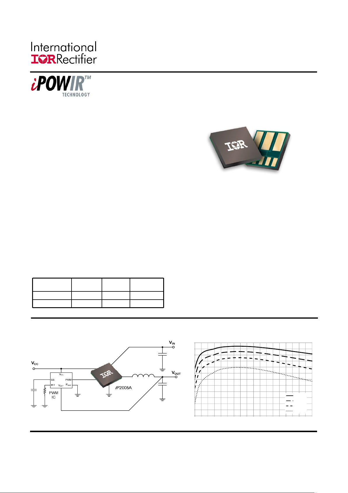
Typical Application
1
iP2005A Product Efficiency
VIN= 12V, FSW= 1MHz, & T
BLK
= 125ºC
70
72
74
76
78
80
82
84
86
88
90
92
94
4 6 8 10121416182022242628303234363840
Effici ency ( % )
Output Current (A)
Vo=3.3V
Vo=2.5V
Vo=1.8V
Vo=1.3V
PD-60325
iP2005APbF
VINto P
GND
…………………………..…..-0.5V to 16.5V
V
DD
to P
GND
………………….…….…….-0.5V to 7.5V
CV
CC
to P
GND
……..….……..…………...-0.5V to 7.5V
PWM to P
GND
…………………….………-0.5V to VDD + 0.5V (Note 1)
ENABLE to P
GND
……………..…………-0.5V to VDD + 0.5V (Note 1)
Storage Temperature …………………..-60ºC to 150ºC
Block Temperature ………….………….-40ºC to 150ºC (Note 2)
ESD Rating……………………………....JEDEC, JESD22-A114 (HBM[4KV], Class 3A)
………………………………..JEDEC, JESD22-A115 (MM[400V], Class C)
MSL Rating………………………..……..3
Reflow Temperature …..………………..260ºC Peak
ABSOLUTE MAXIMUM RATINGS
(Voltages referenced to P
GND
)
CAUTION: Stresses above those listed in “Absolute Maximum Ratings” may cause
permanent damage to the device. This is a stress only rating and operation of the
device at these or any other conditions above those listed in the “Recommended
Operating Conditions” section of this specification is not implied.
Recommended Operating Conditions
PARAMETER MIN TYP MAX UNITS CONDITIONS
Supply Voltage (V
DD
) 4.5 - 7.0 V
Input Voltage (V
IN
) 6.5 - 13.2 V
Output Voltage (V
OUT
)--5.5V
Output Current (I
OUT
)--40A
Switching Frequency 250 - 1500 kHz
On Time Duty Cycle - - 85 %
Minimum V
SW
On Time 60 - - ns VDD= 5.0V, VIN= 12V
Block Temperature (T
BLK
) -40 - 125 ºC (Note 2)
www.irf.com 2/8/2008
2
PD-60325
iP2005APbF
Electrical Specifications
These specifications apply for T
BLK
= 0ºC to 125ºC and VDD= 5.0V unless otherwise specified.
PARAMETER MIN TYP MAX UNITS CONDITIONS
P
LOSS
Power Block Losses - 9.3 11.1 W
V
IN
= 12V, VDD= 5.0V,
V
OUT
= 1.3V, I
OUT
= 40A,
F
SW
= 1MHz,
L
OUT
= 0.3uH, T
BLK
= 25ºC
(Note 3)
V
DD
Supply Current (Stand By)
(I
Q-VDD
)
-2.23mA V
DD
= 5.0, ENABLE = 0V
Supply Current (Operating) - 50 65 mA
V
IN
= 12V, ENABLE = VDD= 5V,
F
SW
= 1MHz, 10% DC
CV
CC
(LDO Output)
Output Voltage 5.5 6.0 6.75 V
Output Current 80 - - mA
Output Capacitor 1.0 - - µF Ceramic, X5R, 16V
Power-On Reset (POR)
V
DD
Rising 3.7 4.1 4.5 V
Hysteresis 140 185 230 mV V
DD
Rising & Falling
CVCC Rising 4.2 4.6 5.0 V
Hysteresis 165 220 275 mV CV
CC
Rising & Falling
ENABLE INPUT
Logic Level Low Threshold (V
IL
)- - 0.8 V
Logic Level High Threshold
(V
IH
)
2.0 - - V
Threshold Hysteresis - 100 - mV
Weak Pull-down Impedance - 100 - kΩ
Rising Propagation Delay
(T
PDH
)
-40-ns
Falling Propagation Delay
(T
PDL
)
-75-ns
Schmitt Trigger Input
V
DD
= POR to 7.0V
www.irf.com 2/8/2008
3
PD-60325
iP2005APbF
2/8/2008www.irf.com
4
PARAMETER MIN TYP MAX UNITS CONDITIONS
PWM INPUT
Logic Level Low Threshold (V
IL
)- - 0.8 V
Logic Level High Threshold
(V
IH
)
2.0 - - V
Threshold Hysteresis - 100 - mV
Weak Pull-down impedance - 100 - kΩ
Rising Propagation Delay
(T
PDH
)
-60-ns
Falling Propagation Delay
(T
PDL
)
-30-ns
Schmitt Trigger Input
V
DD
= POR to 7.0V
(Note 4)
Electrical Specifications (continued)
These specifications apply for T
BLK
= 0ºC to 125ºC and VDD= 5.0V unless otherwise specified.
Notes:
1. Must not exceed 7.5V
2. Block Temperature (T
BLK
) is defined as any Die temperature within the package
3. Measurement made with six 10µF (TDK C3225X5R1C106KT or equivalent) ceramic capacitors placed across VIN to
PGND pins (see Figure 8)
4. Not associated with rise and fall times. Does not affect Power Loss
PD-60325
iP2005APbF
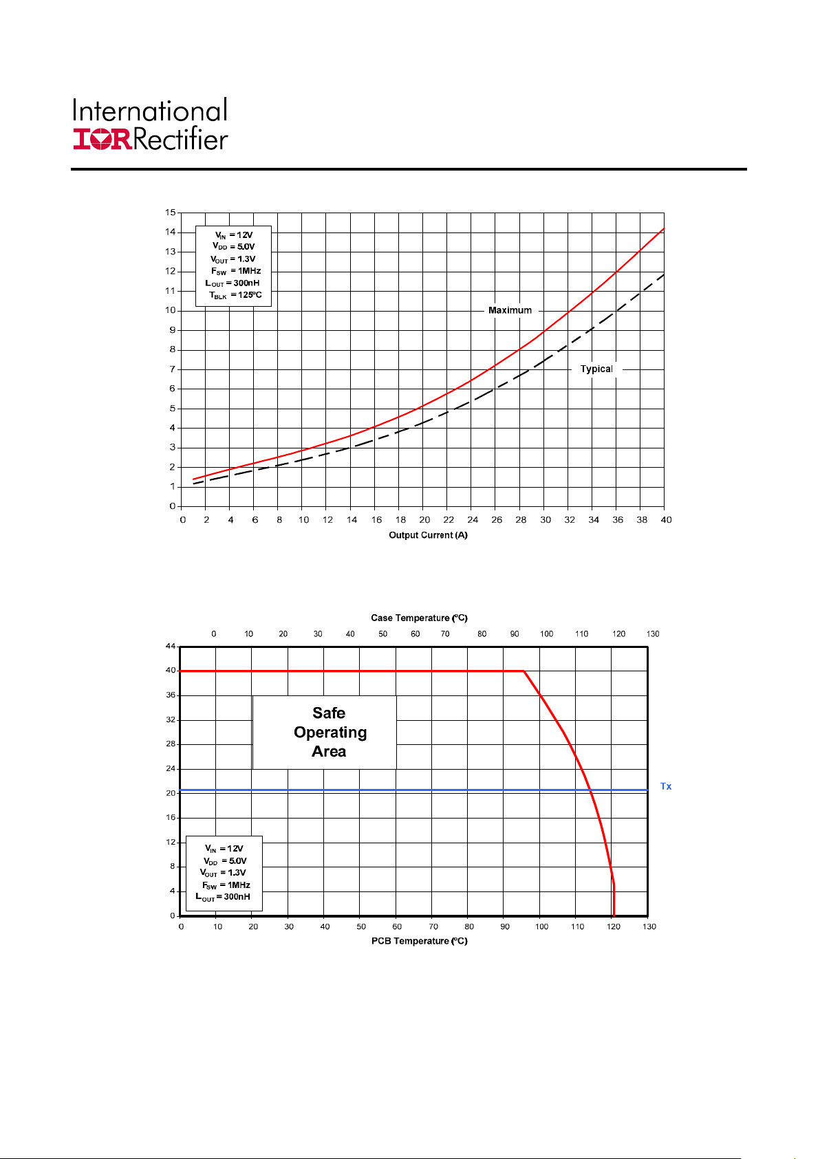
Power Loss Curve
Figure 1 Power Loss Curve
Power Loss (W)
SOA Curve
Figure 2 Safe Operating Area Curve
Output Current (A)
www.irf.com 2/8/2008
5
PD-60325
iP2005APbF
Typical Performance Curves
2/8/2008www.irf.com
6
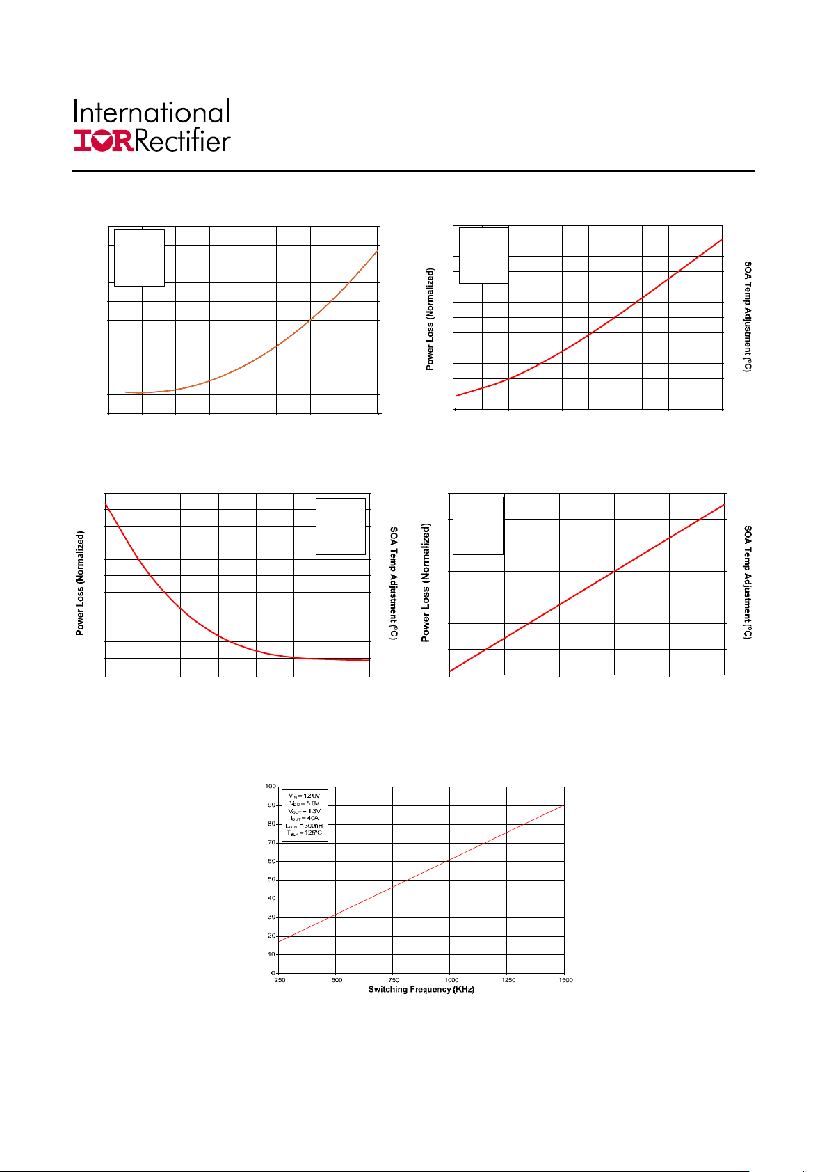
Figure 3 Normalized Power Loss vs. Input Voltage
Power Loss (Normalized)
Figure 4 Normalized Power Loss vs. Output Voltage
0.96
0.98
1.00
1.02
1.04
1.06
1.08
1.10
1.12
1.14
1.16
1.18
1.20
0.8
1.3 1.8 2.3 2.8 3.3
Output Voltage (V)
-0.9
-0.5
0.0
0.5
0.9
1.4
1.9
2.3
2.8
3.3
3.7
4.2
VIN= 12.0V
V
DD
= 5.0V
I
OUT
= 40A
F
SW
= 1MHz
L
OUT
= 300nH
T
BLK
= 125ºC
0.90
0.92
0.94
0.96
0.98
1.00
1.02
1.04
1.06
1.08
1.10
6 7 8 9 10 11 12 13 14
Input Voltage (V)
-2.4
-1.9
-1.4
-1.0
-0.5
0.0
0.5
1.0
1.4
1.9
2.4
SOA Temp Adjustment (ºC)
VDD= 5.0V
V
OUT
= 1.3V
I
OUT
= 40A
F
SW
= 1MHz
L
OUT
= 300nH
T
BLK
= 125ºC
Figure 5 Normalized Power Loss vs. Inductance
Figure 6 Normalized Power Loss vs. Switching Frequency
0.6
0.7
0.8
0.9
1.0
1.1
1.2
1.3
250 500 750 1000 1250 1500
Switching Frequency (kHz)
-10.0
-7.5
-5.0
-2.5
0.0
2.5
5.0
7.5
VIN= 12.0V
V
DD
= 5.0V
V
OUT
= 1.3V
I
OUT
= 40A
L
OUT
= 300nH
T
BLK
= 125ºC
0.96
0.97
0.98
0.99
1.00
1.01
1.02
1.03
1.04
1.05
1.06
1.07
0.1
0.2 0.3 0.4 0.5 0.6 0.7 0.8
Output Inductance (µH)
-1.0
-0.7
-0.5
-0.2
0.0
0.2
0.5
0.7
1.0
1.2
1.4
1.7
VIN= 12.0V
V
DD
= 5.0V
V
OUT
= 1.3V
I
OUT
= 40A
F
SW
= 1MHz
T
BLK
= 125ºC
Figure 7 V
DD
Supply Current vs. Switching Frequency
Average I
DD
(mA)
 Loading...