

PD - 5.029
6,7
Next Data SheetIndex
Previous Datasheet
To Order
CPU165MU
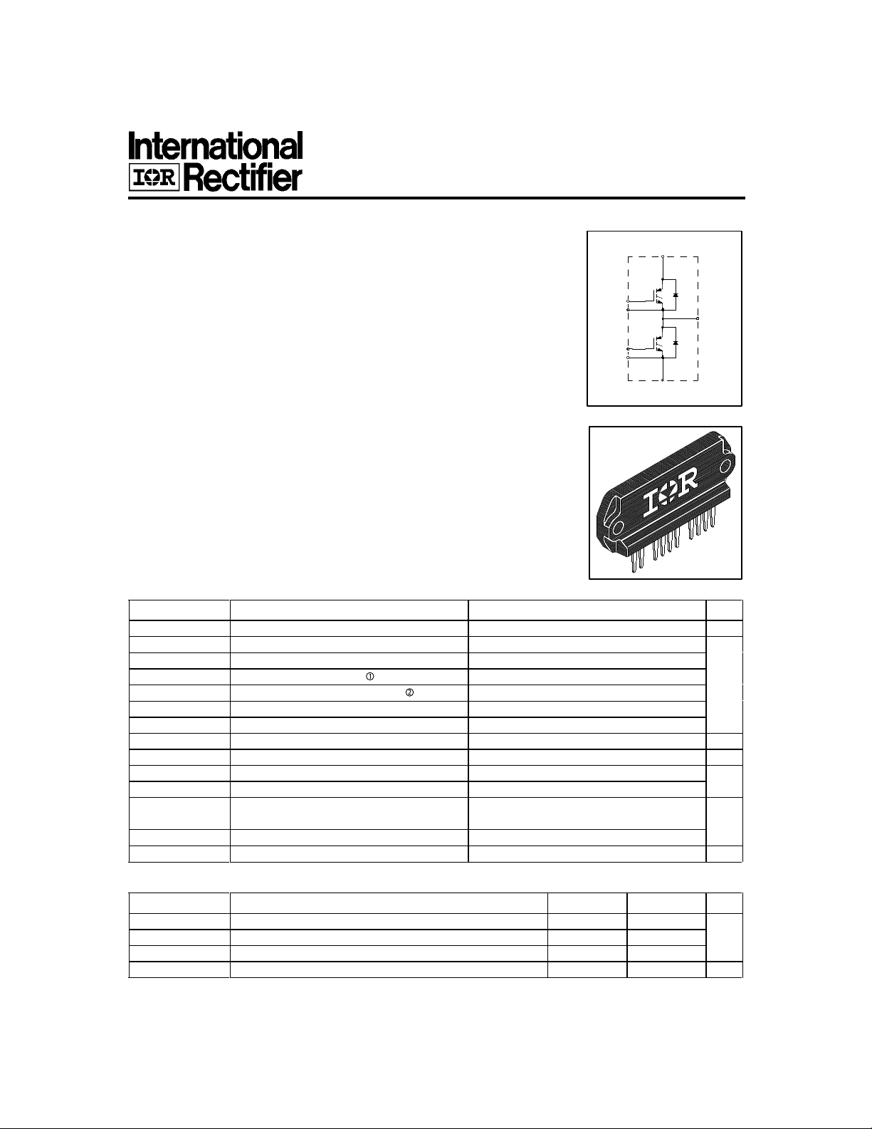
IGBT SIP MODULE
Features
Ultra-Fast IGBT
1,2
• Fully isolated printed circuit board mount package
• Switching-loss rating includes all "tail" losses
• HEXFREDTM soft ultrafast diodes
• Optimized for high operating frequency (over 5kHz)
See Fig. 1 for Current vs. Frequency curve
Product Summary
Q1
4
5
Q2
9
D1
D2
Output Current in a Typical 20 kHz Motor Drive
10 A
with TC = 90°C, TJ = 125°C, Supply Voltage 360Vdc,
RMS
11,12
Power Factor 0.8, Modulation Depth 80% (See Figure 1)
Description
The IGBT technology is the key to International Rectifier's advanced line of
IMS (Insulated Metal Substrate) Power Modules. These modules are more
efficient than comparable bipolar transistor modules, while at the same time
having the simpler gate-drive requirements of the familiar power MOSFET.
This superior technology has now been coupled to a state of the art materials
system that maximizes power throughput with low thermal resistance. This
package is highly suited to motor drive applications and where space is at a
premium.
IMS-1
Absolute Maximum Ratings
Parameter Max. Units
V
CES
IC @ TC = 25°C Continuous Collector Current, each IGBT 33
IC @ TC = 100°C Continuous Collector Current, each IGBT 17
I
CM
I
LM
IF @ TC = 100°C Diode Continuous Forward Current 15
I
FM
V
GE
V
ISOL
PD @ TC = 25°C Maximum Power Dissipation, each IGBT 83 W
PD @ TC = 100°C Maximum Power Dissipation, each IGBT 33
T
J
T
STG
Collector-to-Emitter Voltage 600 V
Pulsed Collector Current 100 A
Clamped Inductive Load Current 100
Diode Maximum Forward Current 100
Gate-to-Emitter Voltage ±20 V
Isolation Voltage, any terminal to case, 1 minute 2500 V
Operating Junction and -40 to +150
Storage Temperature Range °C
Soldering Temperature, for 10 sec. 300 (0.063 in. (1.6mm) from case)
Mounting torque, 6-32 or M3 screw. 5-7 lbf•in (0.55-0.8 N•m)
RMS
Thermal Resistance
R
(IGBT) Junction-to-Case, each IGBT, one IGBT in conduction — 1.5
θJC
R
(DIODE) Junction-to-Case, each diode, one diode in conduction — 2.0 °C/W
θJC
R
(MODULE) Case-to-Sink,flat,greased surface 0.1 —
θCS
Wt Weight of module 20 (0.7) — g (oz)
Parameter Typ. Max. Units
Revision 1
C-733
CPU165MU
Next Data SheetIndex
Previous Datasheet
To Order
Electrical Characteristics @ TJ = 25°C (unless otherwise specified)
Parameter Min. Typ. Max. Units Conditions
V
(BR)CES
∆V
(BR)CES
V
CE(on)
V
GE(th)
∆V
GE(th)
g
fe
I
CES
V
FM
I
GES
Switching Characteristics @ TJ = 25°C (unless otherwise specified)
Parameter Min. Typ. Max. Units Conditions
Q
g
Q
ge
Q
gc
t
d(on)
t
r
t
d(off)
t
f
E
on
E
off
E
ts
t
d(on)
t
r
t
d(off)
t
f
E
ts
C
ies
C
oes
C
res
t
rr
I
rr
Q
rr
di
(rec)M
Collector-to-Emitter Breakdown Voltage 600 — — V VGE = 0V, IC = 250µA
/∆T
Temperature Coeff. of Breakdown Voltage — 0.60 — V/°C VGE = 0V, IC = 1.0mA
J
Collector-to-Emitter Saturation Voltage — 1.8 2.3 IC = 17A VGE = 15V
— 2.2 — V IC = 33A See Fig. 2, 5
— 1.6 — IC = 17A, TJ = 150°C
Gate Threshold Voltage 3.0 — 5.5 VCE = VGE, IC = 250µA
/∆TJTemperature Coeff. of Threshold Voltage — -13 — mV/°C VCE = VGE, IC = 250µA
Forward Transconductance 16 24 — S VCE = 100V, IC = 27A
Zero Gate Voltage Collector Current — — 250 µA VGE = 0V, VCE = 600V
— — 6500 VGE = 0V, VCE = 600V, TJ = 150°C
Diode Forward Voltage Drop — 1.3 1.7 V IC = 25A See Fig. 13
— 1.2 1.5 IC = 25A, TJ = 150°C
Gate-to-Emitter Leakage Current — — ±500 nA VGE = ±20V
Total Gate Charge (turn-on) — 108 140 IC = 27A
Gate - Emitter Charge (turn-on) — 17 21 nC VCC = 400V
Gate - Collector Charge (turn-on) — 52 70 See Fig. 8
Turn-On Delay Time — 23 — TJ = 25°C
Rise Time — 28 — ns IC = 27A, VCC = 480V
Turn-Off Delay Time — 100 200 VGE = 15V, RG = 5.0Ω
Fall Time — 45 140 Energy losses include "tail" and
Turn-On Switching Loss — 0.76 — diode reverse recovery.
Turn-Off Switching Loss — 0.26 — mJ See Fig. 9, 10, 11, 18
Total Switching Loss — 1.0 2.0
Turn-On Delay Time — 24 — TJ = 150°C, See Fig. 9, 10, 11, 18
Rise Time — 27 — ns IC = 27A, VCC = 480V
Turn-Off Delay Time — 180 — VGE = 15V, RG = 5.0Ω
Fall Time — 130 — Energy losses include "tail" and
Total Switching Loss — 3.7 — mJ diode reverse recovery.
Input Capacitance — 2900 — VGE = 0V
Output Capacitance — 330 — pF VCC = 30V See Fig. 7
Reverse Transfer Capacitance — 41 — ƒ = 1.0MHz
Diode Reverse Recovery Time — 50 75 ns TJ = 25°C See Fig.
— 105 160 TJ = 125°C 14 IF = 25A
Diode Peak Reverse Recovery Current — 4.5 10 A TJ = 25°C See Fig.
— 8.0 15 TJ = 125°C 15 VR = 200V
Diode Reverse Recovery Charge — 112 375 nC TJ = 25°C See Fig.
— 420 1200 TJ = 125°C 16 di/dt = 200A/µs
/dt Diode Peak Rate of Fall of Recovery — 250 — A/µs TJ = 25°C See Fig.
During t
b
— 160 — TJ = 125°C 17
Notes:
Repetitive rating; VGE=20V, pulse width
limited by max. junction temperature.
( See fig. 20 )
VCC=80%(V
), VGE=20V, L=10µH,
CES
RG= 5.0Ω, ( See fig. 19 )
Pulse width ≤ 80µs; duty factor ≤ 0.1%.
C-734
Pulse width 5.0µs,
single shot.
CPU165MU
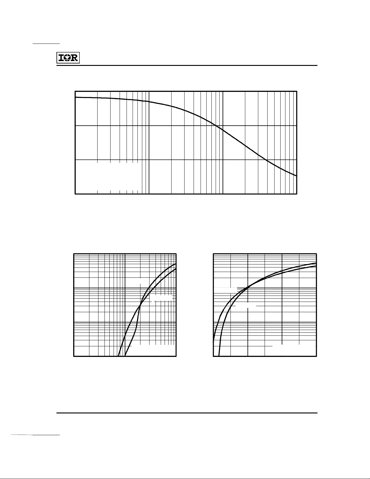
f, Frequency (kHz)
Load Current (A)
Total Output Power (kW)
20
CE
C
I , Collector-to-Emitter Current (A)
, Collector-to-Em
er Voltage (V)
To Order
Next Data SheetIndex
Previous Datasheet
24
16
8
T = 90°C
C
T = 125°C
J
Power Factor = 0.8
Modulation Depth = 0 .8
V = 60% of Rated Voltage
CC
0
0.1 1 10 100
Fig. 1 - RMS Current and Output Power, Synthesized Sine Wave
1000
1000
7.4
5.0
S
2.5
0
100
10
1
0.1 1 1 0
V
Fig. 2 - Typical Output Characteristics
T = 25°C
J
T = 150°C
J
V = 15V
G E
20µs P UL SE WIDTH
itt
C-735
100
T = 150°C
J
T = 25°C
J
10
C
I , Collector-to-Emitter Current (A)
1
5 10 15
V , Gate-to-Emitter Voltage (V)
GE
V = 100V
CC
5µs PULSE WIDTH
Fig. 3 - Typical Transfer Characteristics

CPU165MU
t , Rectangular Pulse Duration (sec)
1
thJC
Thermal Response (Z )
Maximum DC Collector Current (A)
, Case Tempera ture (°C)
C
, Case Temperature (°C)
C
CE
V , Collector-to-Emitter Voltage (V)
To Order
Next Data SheetIndex
Previous Datasheet
60
50
40
30
20
10
0
25 50 7 5 100 125 1 5 0
V = 15V
GE
T
Fig. 4 - Maximum Collector Current vs.
Case Temperature
1
3.0
V = 15V
G E
80 µs P ULSE W IDTH
2.5
2.0
1.5
1.0
-6 0 -4 0 -2 0 0 20 40 60 80 10 0 120 1 4 0 160
I = 54A
C
I = 27A
C
I = 14A
C
T
Fig. 5 - Collector-to-Emitter Voltage vs.
Case Temperature
D = 0.50
0.1
0.01
0.0 0 001 0.0001 0.0 0 1 0.01 0.1 1 10
Fig. 6 - Maximum IGBT Effective Transient Thermal Impedance, Junction-to-Case
0.2 0
0.1 0
0.05
0.0 2
0.0 1
SIN GLE PUL SE
(THERMAL RESPONS E )
C-736
P
DM
Note s:
1. Duty facto r D = t / t
2. Peak T = P x Z + T
J
DM
2
1
thJC
t
1
t
2
C

CPU165MU
CE
C, Capacitance (pF)
, Collector-to-Em
er Voltage (V)
GE
V , Gate-to-Emitter Voltage (V)
, Total Gate Charge (nC)
g
Total Switching Losses (mJ)
W
, Case Tempera ture (°C)
Total S witching Losses (m J)
To Order
Next Data SheetIndex
Previous Datasheet
7000
6000
5000
4000
3000
2000
1000
0
1 10 100
V = 0V, f = 1MHz
GE
C = C + C , C SHORTED
ies ge gc ce
C = C
res gc
C = C + C
oes ce gc
C
ies
C
oes
C
res
V
itt
Fig. 7 - Typical Capacitance vs.
Collector-to-Emitter Voltage
2.50
V = 480V
CC
V = 15V
G E
T = 25 °C
C
I = 27A
C
2.25
20
V = 480V
CE
I = 27A
C
16
12
8
4
0
0 30 60 90 120
Q
Fig. 8 - Typical Gate Charge vs.
Gate-to-Emitter Voltage
10
R = 2.0
V = 15V
V = 480V
G
GE
CC
Ω
I = 5 4A
C
2.00
1.75
1.50
0 10 2 0 3 0 40 5 0
Fig. 9 - Typical Switching Losses vs. Gate
R , Gate Resistance ( )
G
Resistance
I = 27A
C
1
I = 14A
C
0.1
-6 0 -40 -20 0 20 40 6 0 8 0 100 120 1 40 160
Ω
T
C
Fig. 10 - Typical Switching Losses vs.
Case Temperature
C-737

CPU165MU
Total Switching Losses (mJ)
, Collector-to-Em
er Current (A)
C
CE
,
)
I , C ollec tor-to-E mitter Current (A)
To Order
Next Data SheetIndex
Previous Datasheet
6.0
R = 2.0
G
T = 150°C
C
V = 4 80 V
CC
5.0
V = 15V
G E
4.0
3.0
2.0
1.0
0.0
0 10 20 30 40 5 0 60
Ω
I
C
itt
Fig. 11 - Typical Switching Losses vs.
Collector-to-Emitter Current
100
1000
V = 20V
G E
GE
T = 125°C
J
100
10
1
1 10 100 1000
V
S AFE OPE RATIN G A REA
C ollector-to-E m itt er V oltage (V
Fig. 12 - Turn-Off SOA
F
T = 150°C
J
T = 125°C
J
10
T = 25°C
J
Instantaneous Forward Current - I (A)
1
0.6 1.0 1.4 1.8 2.2 2.6
Forward Volt age Drop - V (V)
FM
Fig. 13 - Maximum Forward Voltage Drop vs. Instantaneous Forward Current
C-738

CPU165MU
To Order
Next Data SheetIndex
Previous Datasheet
140
V = 200V
R
T = 125°C
J
T = 25°C
120
100
I = 50A
80
rr
t - (ns)
F
I = 25A
F
I = 10A
F
60
40
20
100 1000
di /dt - (A/µs)
f
J
Fig. 14 - Typical Reverse Recovery vs. dif/dt
1500
V = 200V
R
T = 125°C
J
T = 25°C
J
1200
100
V = 200V
R
T = 125°C
J
T = 25°C
J
I = 50A
F
I = 25A
F
10
IRRM
I - (A)
1
100 1000
di /dt - (A/µs)
f
I = 10A
F
Fig. 15 - Typical Recovery Current vs. dif/dt
10000
V = 200V
R
T = 125°C
J
T = 25°C
J
900
RR
Q - (nC)
600
I = 25A
F
300
0
100 1000
Fig. 16 - Typical Stored Charge vs. dif/dt Fig. 17 - Typical di
I = 50A
F
di /dt - (A/µs)
I = 10A
1000
F
di(rec)M/dt - (A/µs)
I = 25A
F
I = 10A
F
100
100 1000
f
I = 50A
F
di /dt - (A/µs)
f
/dt vs. dif/dt
(rec)M
C-739

CPU165MU
To Order
Next Data SheetIndex
Previous Datasheet
Same type
device as
D.U.T .
90% Vge
+Vge
Vce
80%
of Vce
430µF
D.U.T.
Fig.18a - Test Circuit for Measurement of
ILM, Eon, E
off(diode)
, trr, Qrr, Irr, t
d(on)
, tr, t
d(off)
, t
f
Fig. 18b - Test Waveforms for Circuit of Fig. 18a, Defining
GATE VOLTAGE D.U.T.
Vcc
10% +Vg
10% Ic
td(on)
Vce
tr
t1
90% Ic
5% Vce
+Vg
DUT VOLTAGE
AND CURRENT
Ipk
Ic
t2
Vce ie dt
Eon =
∫
t1
t2
Fig. 18c - Test Waveforms for Circuit of Fig. 18a,
Defining Eon, t
d(on)
, t
r
10% Vce
Ic
td(off)
t1
E
Ic
tx
10% Vcc
Vpk
DIODE REVERSE
RECOVERY ENERGY
Irr
, t
off
d(off)
trr
t3
90% Ic
Ic
5% Ic
tf
t1+5µS
Vce ic dt
Eoff =
∫
t1
t2
, t
f
trr
Qrr =
id dt
∫
tx
10% Irr
Vcc
DIODE RECOVERY
WAVEFORMS
t4
Erec =
Vd id dt
∫
t3
t4
Fig. 18d - Test Waveforms for Circuit of Fig. 18a,
Defining E
, trr, Qrr, I
rec
rr
Refer to Section D for the following:
Appendix D: Section D - page D-6
Package Outline 4 - IMS-1 Package (10 pins) Section D - page D-13
Fig. 18e - Macro Waveforms for Test Circuit of Fig. 18a
Fig. 19 - Clamped Inductive Load Test Circuit
Fig. 20 - Pulsed Collector Current Test Circuit
C-740
 Loading...