

Page 1

Zx10
System Board Manual
May 2000
D1AA0035A
Page 2

Copyright
2000 Intergraph Computer Systems. All rights reserved. This document contains information protected by
copyright, trade secret, and trademark law. This document may not, in whole or in part, be reproduced in any form or
by any means, or be used to make any derivative work, without written consent from Intergraph Computer Systems.
Use, duplication, or disclosure by the United States Government is subject to restrictions as set forth in subdivision
(c)(1)(ii) of the rights in technical data and computer software clause at DFARS 252.227-7013. Unpublished rights are
reserved under the copyright laws of the United States.
Intergraph Computer Systems, Huntsville AL 35894-0001
Notice
Information in this document is subject to change without notice and should not be considered a commitment by
Intergraph Computer Systems. Intergraph Computer Systems shall not be liable for technical or editorial errors in, or
omissions from, this document. Intergraph Computer Systems shall not be liable for incidental or consequential
damages resulting from the furnishing or use of this document.
All warranties given by Intergraph Computer Systems about equipment or software are set forth in your purchase
contract. Nothing stated in, or implied by, this document or its contents shall be considered or deemed a modification
or amendment of such warranties.
Trademarks
Intergraph and the Intergraph logo are registered trademarks of Intergraph Corporation. Zx is a trademark of
Intergraph Computer Systems. Intel and Pentium are registered trademarks of Intel Corporation. ServerSet is a
trademark of ServerWorks Corporation. Microsoft is a registered trademark of Microsoft Corporation. Other brands
and product names are trademarks of their respective owners.
FCC/DOC Compliance
This equipment has been tested and found to comply with the limits for a Class B digital device, pursuant to part 15 of
the FCC Rules. These limits are designed to provide reasonable protection against harmful interference when the
equipment is operated in a residential installation. This equipment generates, uses, and can radiate radio frequency
energy. If the equipment is not i nstalled and used in accordance with the inst ructions, it may cause harmful
interference to radio communications. However, there is no guarantee that interference will not occur in a particular
installation.
If this equipment does cause h armful int erference t o radio or television reception, which can be d et ermined by turning
the equipment off and on, try to correct the interference as follows: reorient or relocate the affected device; increase
the separation between this equipment and the affected device; connect this equipment to an outlet on a circuit different
from the circuit to which the affected device is connected ; consult a dealer or an experienced radio/television
technician for help.
This Class B digital apparatus meets all requirements of the Canadian Interference-Causing Equipment Regulations.
Cet appareil numérique de la classe B respecte toutes les exigencies du Règlement sur le materiél brouilleur du Canada.
Page 3

Safety Notices
Service and upgrade tasks should be performed by users who can follow instructions in a manual to service equipment,
and can do so without harm to themselves or damage to the equipment.
To reduce the risk of electrical sh ock and energy hazards, do not attempt to open the equipment unless instructed, and
do not use a tool for purposes other than instructed.
Internal components may be at high temperatures. Allow time for them to cool before handling them.
Internal components can be damaged by static electricity. Use an antistatic wrist strap connected to the bare metal of
the system’s chassis to protect against electrostatic discharge.
Notes
Changes or modifications made to the system that are not approved by the party responsible for compliance could void
the user's authority to operate the equipment.
Procedures in this document assume familiarity with the general terminology associated with personal computers, and
with the safety practices and regulatory compliance required for using and modifying electronic equipment.
Read all operating instructions before using this device. Keep these instructions for future reference. Follow all
warnings on the device or in the operating instructions.
Page 4

Page 5

Contents
Preface...........................................................................................................................................vii
About This Document.....................................................................................................................vii
Document Conventions...................................................................................................................vii
Customer Support...........................................................................................................................vii
1 Overview....................................................................................................................................... 1
Features and Components................................................................................................................. 1
Block Diagrams................................................................................................................................ 3
Major Components........................................................................................................................... 6
2 Components..................................................................................................................................7
Processors......................................................................................................................................... 7
Memory Modules..............................................................................................................................9
Expansion Sockets.......................................................................................................................... 13
Power and Data Connectors............................................................................................................14
Fan Connectors............................................................................................................................... 14
ATAPI Connectors......................................................................................................................... 16
Jumper Connectors......................................................................................................................... 17
I/O Port Connectors........................................................................................................................ 18
Integrated Controllers..................................................................................................................... 22
Hardware Monitoring and Power Management.............................................................................. 24
CMOS/Clock Lithium Battery........................................................................................................ 26
v
Keyboard, Mouse............................................................................................................. 19
Parallel ............................................................................................................................. 19
Serial ................................................................................................................................ 20
Universal Serial Bus......................................................................................................... 20
Ethernet Network ............................................................................................................. 20
External Wide Ultra2 SCSI (LVDS)................................................................................ 21
Audio Line Out, Line In, Microphone.............................................................................. 21
SCSI Controller................................................................................................................ 22
Network Controller...........................................................................................................23
Audio Controller .............................................................................................................. 23
3 BIOS Setup................................................................................................................................. 27
BIOS Overview.............................................................................................................................. 27
Using BIOS Setup .......................................................................................................................... 27
BIOS Setup Screens........................................................................................................................28
Main Screen.................................................................................................................................... 28
Advanced Screen............................................................................................................................ 29
Security Screen............................................................................................................................... 30
Misc. Screen................................................................................................................................... 30
Boot Screen .................................................................................................................................... 31
Exit Screen...................................................................................................................................... 31
Using CMOS Reset.........................................................................................................................32
Updating the System BIOS ............................................................................................................. 32
Page 6

vi
4 Resources.................................................................................................................................... 33
ISA Interrupt Requests (IRQs) ....................................................................................................... 33
PCI-to-ISA Interrupt Map...............................................................................................................34
Direct Memory Access (DMA) Channels....................................................................................... 34
Input/Output (I/O) Map.................................................................................................................. 35
Memory Map.................................................................................................................................. 37
5 Messages..................................................................................................................................... 39
POST Tasks and Beep Codes......................................................................................................... 39
Error Messages............................................................................................................................... 43
Page 7

Preface
This System Board Manual provides detailed information on the Intergraph Computer Systems
Zx
10 system board.
About This Document
This System Board Manual is organized as follows:
♦ Chapter 1, “Overview,” introduces the system board, its features, and its major components.
♦ Chapter 2, “Components,” locates and describes the major components on the system board.
♦ Chapter 3, “BIOS Setup,” describes the BIOS Setup program and the system’s BIOS settings.
♦ Chapter 4, “Resources,” lists and describes system board resources.
♦ Chapter 5, “Messages,” lists and describes messages pr oduced by the system board.
Document Conventions
vii
Bold
Italic Variable values that you supply, or cross-references.
Monospace
SMALL CAPS Key names on the keyboard (such as D, ALT, or F3) and names of files and
CTRL+D Press a key while simultaneously pressing another key; for example, press CTRL
Commands, words, or characters that you key in literally.
Output displayed on the screen.
directories. You can type filenames and directory names in the dialog boxes or
the command line in lowercase unless directed otherwise.
and D simultaneously.
Customer Support
Intergraph Computer Systems hardware has a factory warranty ranging from 30 days to three years.
A detailed warranty description is available on the World Wide Web. You can also take advantage
of other available hardware support services.
Intergraph Computer Systems provides complimentary operating system and system software
support for 30 or 90 days following shipment of a hardware or software product. At the end of the
complimentary support period, you can take advantage of other levels of software support.
Page 8

viii
To get more information on support services:
♦ Visit the Support pages on the World Wide Web at http://www.intergraph.com/ics.
♦ In the United States, call 1-800-414-8991.
♦ Outside the United States, contact your local Intergraph Computer Systems subsidiary or
distributor.
To visit Intergraph Computer Systems on the World Wide Web:
Use your World Wide Web browser to go to http://www.intergraph.com/ics.
To get customer support by telephone:
♦ In the United States, call 1-800-633-7248 between the hours of 7:00 a.m. and 7:00 p.m.
Central Time, Monday through Friday (e xcept holidays).
♦ Outside the United States, contact your local Intergraph Computer Systems subsidiary or
distributor.
♦ Have the following information available when you call:
− Your service number, which identifies your site to Intergraph Computer Systems. You
use your service number for warranty or maintenance calls.
− Your Customer Personal Identification Number (CPIN). You get a CPIN the first time
you call the Customer Response Center; it is associated with your service number for
future call logging.
− The product’s name or model number.
− The product’s serial number. Software product serial numbers are included in the product
packaging. Hardware product serial numbers are on a sticker affixed to the hardware
product.
− Your name and telephone number.
− A brief description of the question or problem.
Page 9

1Overview
This chapter describes the system board, its features, and its major components.
Features and Components
1
Processors
System Chipset
I/O Controller
Memory
Dual Intel SC242 (Slot 1) support
Intel Pentium III processors
Two integrated voltage regul ators
64-bit front-side bus (FSB) – 133 MHz or 100 MHz (varies by system)
ServerWorks ServerSet III WS
Streaming Multiport Controllers
32-bit fast I/O interface – 266 MHz (for 133 MHz FSB) or 200 MHz
(for 100 MHz FSB)
AGP controller – one AGP Pro expansion socket
USB controller – four Universal Serial Bus (USB) ports – two external,
one internal, one for the AGP controller
EIDE controller – two Peripheral Component Interconnect (PCI)
bus-mastering EIDE channels
SMC FDC37B787
Controls keyboard, mouse, real-time clock, and floppy disk
Two serial ports, one parallel port
Synchronous Dynamic Random Access Memory (SDRAM) – PC133 or
PC100 (to match FSB speed)
Six (133 MHz FSB) or eight (100 MHz FSB) 168-pin registered dualinline memory module (DIMM) sockets
Supports 72-bit Error Correction Code (ECC) memory modules
Four banks, two DIMMs per bank, two-way interleaved
128-bit memory bus – 133 MHz or 100 MHz (to match FSB speed)
SCSI Controller
LSI 53C1010
Low-voltage differential (LVD) Ultra 3 SCSI bus
Two 16-bit 80 MHz SCSI channels
Two high-density (HD) 68-pin SCSI connect ors
320 MB/sec Ultra 3 SCSI throughput
Handles both Ultra2 and Ultra3 devices at their assigned transfer rates
Page 10

2
Network Controller
Audio Controller
Expansion Sockets
Input/Output Ports
Intel 82559
100 Mbit/sec and 10 Mbit/sec Ethernet network interface
Wake-on-Modem support
Wake-on-LAN support
Creative Labs ES1373 AudioPCI
Audio Codec ’97 (AC97)
Advanced Technology Attachment Packet Interface (ATAPI) CD-ROM
audio header, modem audio header, and video header
One full-length AGP Pro socket
Two full-length fast/wide PCI sockets (64 bits, 66 MHz/33 MHz, 3.3 V)
Four full-length wide PCI sockets (64 bits, 33 MHz, 5 V)
One full-length Industry Standard Architecture (ISA) socket (16 bits)
One PS/2 mouse port (6-pin mini-DIN)
One PS/2 keyboard port (6-pin mini-DIN)
One parallel (LPT) port (25-pin D-sub)
Two serial (COM) ports (9-pin D-sub)
Two USB po rts (self-ide ntifying, hot-pluggabl e, 12 MB/s ec)
One SCSI port (68-pin HD) – Ultra 3
One Ethernet port (8-pin RJ-45)
One each microphone in, line in, and line out audio ports (PC standard
1/8-inch phone jacks)
One MIDI/game port (15-pin D-sub)
Four ATAPI connectors (internal) – CD IN, VIDEO IN, MONO IN,
MPEG IN
BIOS
Form Factor
Phoenix BIOS
Supports Advanced Configuration and Power Interface (ACPI)
Supports Desktop Management Interface (DMI)
Supports PC99
Supports S0, S1, S3, and S5 system states
Auto-configuration of IDE hard disk types
Extended ATX (12 in x 13 in)
Two 20-pin ATX power connectors
Stacked input/output ports
Page 11

3
Voltage and Power
System Management
Regulatory Compliance
Block Diagrams
The diagrams on the following pages show the system board components and connections for the
133 MHz and 100 MHz system boards.
ATX power supply connectors
+12V variable power source for DC fans
3.3 V SDRAM memory support
Monitoring of all system voltages and four temperature p oints
Fan headers with monitor i ng and control functions
Chassis intrusion alert header
Temperatur e and voltage monitoring
Wake-on-Modem header
Wake-on-LAN hea der
FCC Class B (Declaration of Conformity)
European Community CE (Declaration of Conformity)
Underwriter’s Laboratories
Page 12

4
Mouse /
Keyboard
USB
x2
Serial x2 / Parallel
Out/ Mic. / MIDI
Audio Line In / Line
10/100
Ethernet
AC97
Codec
Wahoo 133MHz FSB
Block Diagram
CPU 2 (SC242)
133MHz, 128-bit
Host bus
133MHz, 64-bit
CPU 1 (SC242)
AGP Pro (Slot 0)
PCI (Slot 1)
PCI (Slot 2)
PCI (Slot 3)
ServerWorks
ServerSet III WS
North Bridge
16-bit
16-bit
64-bit
AGP bus
266MHz, 32-bit I/O Link
MEM_DATA
64-bit
MEM_CNTRL
Intel
82559
Ethernet
Ctrl.
16-bit
SDRAM Memory Bank 3
MEM_DATA
SDRAM Memory Bank 1
SDRAM Memory Bank 2 / Not used for 133MHz FSB
ServerWorks
ServerSet III
SDRAM Memory Bank 3
SDRAM Memory Bank 0
Control
Address
WS
MADP
Ensoniq
ES1373
Audio Ctrl.
ATX Power
ATX Power
Floppy
Secondary
LSI
53C1010
Ultra3
IDE
Primary
IDE
Ultra3 SCSI
Channel B
Ultra3 SCSI
Channel A
SDRAM Memory Bank 0
SDRAM Memory Bank 1
SDRAM Memory Bank 2 / Not used for 133MHz FSB
SCSI Ctrl.
Super I/O
Ctrl.
BIOS
Flash
PROM
PCI (Slot 4)
PCI (Slot 5)
PCI (Slot 6)
ISA (Slot 6)
66MHz, 64-bit
33MHz, 64-bit
33MHz, 64-bit
Battery
16-bit
ServerWorks
ServerSet III
WS
I/O Bridge
ServerWorks
ServerSet III
WS
South Bridge
33MHz, 64-bit
Page 13

5
Mouse /
Keyboard
USB
x2
Serial x2 / Parallel
Out/ Mic. / MIDI
Audio Line In / Line
10/100
Ethernet
AC97
Codec
Wahoo 100MHz FSB
Block Diagram
CPU 2 (SC242)
100MHz, 128-bit
Host bus
100MHz, 64-bit
CPU 1 (SC242)
AGP Pro (Slot 0)
PCI (Slot 1)
PCI (Slot 2)
PCI (Slot 3)
ServerWorks
ServerSet III WS
North Bridge
16-bit
16-bit
64-bit
AGP bus
200MHz, 32-bit I/O Link
MEM_DATA
64-bit
MEM_CNTRL
Intel
82559
Ethernet
Ctrl.
16-bit
SDRAM Memory Bank 3
MEM_DATA
SDRAM Memory Bank 1
SDRAM Memory Bank 2
ServerWorks
ServerSet III
SDRAM Memory Bank 3
SDRAM Memory Bank 0
Control
Address
WS
MADP
Ensoniq
ES1373
Audio Ctrl.
ATX Power
ATX Power
Floppy
Secondary
LSI
53C1010
Ultra3
IDE
Primary
IDE
Ultra3 SCSI
Channel B
Ultra3 SCSI
Channel A
SDRAM Memory Bank 0
SDRAM Memory Bank 1
SDRAM Memory Bank 2
SCSI Ctrl.
Super I/O
Ctrl.
BIOS
Flash
PROM
PCI (Slot 4)
PCI (Slot 5)
PCI (Slot 6)
ISA (Slot 6)
33MHz, 64-bit
33MHz, 64-bit
33MHz, 64-bit
Battery
16-bit
ServerWorks
ServerSet III
WS
I/O Bridge
ServerWorks
ServerSet III
WS
South Bridge
33MHz, 64-bit
Page 14
6
)
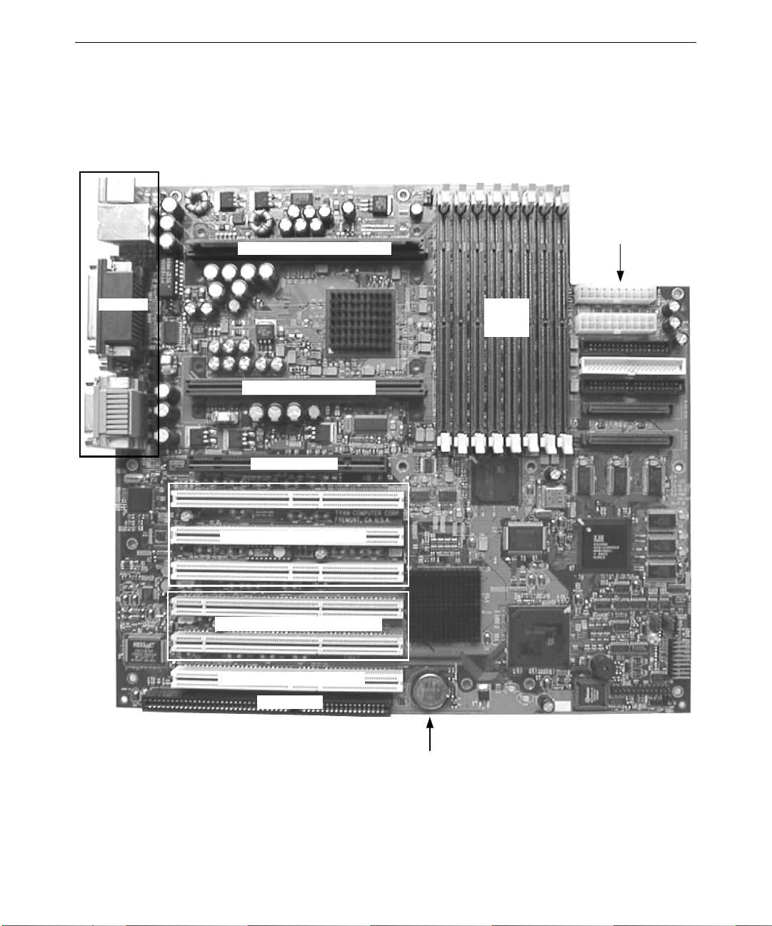
Major Components
The following figure calls out the system board’s major components. More detailed information
on system board components is found in Chapter 2, “Components.”
Secondary Processor Socket
Power & Data
Connectors
I/O Ports
Memory
Module
Sockets
Primary Processor Socket
AGP Pro Socket
PCI Sockets (64-bit 33 MHz
PCI Sockets (64-bit 66/33 MHz)
PCI Socket (64-bit 33 MHz)
ISA Socket
CMOS/Clock Battery
Page 15

2 Components
This chapter locates and describes major components on the system board. The chapter also
provides information on the integrated controllers and hardware monitoring.
WARNING Before touching the system board or its components, disconnect the system’s
power cord from its AC power outlet.
WARNING System board components may be at high temperatures. Allow time for them
to cool before handling them.
WARNING System board components can be damaged by static electricity. Use an
antistatic wrist strap connected to the bare metal of the system’s chassis to
protect against electrostatic discharge.
Processors
The system board contains two Intel SC242 (Slot 1) processor sockets. Each socket has an
associated voltage regulator integrated on the system board.
7
Secondary Processor Socket
Primary Processor Socket
Page 16

8
Each processor socket accepts an Intel Pentium III processor (100 MHz or 133 MHz front-side
bus). The processor is secured to the socket by retention clips on both sides. T he retention clips
are secured by nuts to screws attached to the system board.
Processor
Retention Clip
(One each side)
Processor
The system can function with one or two processors installed. For a single-processor system, a
processor bus terminator card must be installe d in the unused processor socket. For a dualprocessor system, both p rocessors must be the same speed.
Processor Bus Terminator Card
Page 17

Memory Modules
The system board includes sockets for up to six PC133 or eight PC100 dual inline memory
modules (DIMMs). The memory speed matches the system board’s front-side bus speed.
Memory module sockets a re organized into four banks (Bank 0 through Bank 3) of two socket s
each that use two-way memory interleaving.
Bank 2
Bank 3
Bank 1
9
Bank 0
Bank 3
Bank 2
Bank 1
Bank 0
Page 18

10
Each socket accepts a 168-pin registered Synchronous Dynamic RAM (SDRAM) DIMM. Each
DIMM has a 128-bit memory width and 16-bit error correcting code (ECC) protection.
DIMMs in
Bank 0
Each socket is keyed for proper DIMM insertion. Release tabs on each end of the socket capture
the DIMM and secure it in the socket.
DIMM
Release Tab
Notch
DIMM socket
Page 19

On system boards with a 133 MHz front-side bus (FSB), DIMM terminator modules are installed
in Bank 1 instead of standard DIMMs.
DIMM
Terminator
Module
To avoid damaging a DIMM and voiding its warranty, take the following precautions:
♦ Do not remove the DIMM from its antistatic package until you are ready to install it.
♦ Do not touch the metallic finger contacts.
♦ Do not bend, twist, drop, or otherwise handle the DIMM carelessly.
♦ Do not expose the DIMM to moisture or extreme temperatures.
When adding or replacing system memory on all system boards:
11
♦ On a 100 MHz FSB system board, install DIMMs in order from the lowest bank to the highest
bank, starting with ba nk 0.
♦ On a 133 MHz FSB system board, install DIMMs first in Bank 3, then in Bank 2, and finally
in Bank 0. Do not install DIMMs in Bank 1.
♦ On a 133 MHz FSB system board, do not replace DIMM terminator modules in Bank 1 with
standard DIMMs.
♦ Ensure all installed DIMMs are PC133 (133 MHz FSB system board) or PC100 (100 MHz
FSB system board), as appropriate. Do not mix DIMMs of different speeds.
♦ Use only registered DIMMs. Do not use unbuffere d DIMMs.
♦ Install DIMMs in both sockets of a bank. Do not install only one DIMM in a bank.
♦ Install the same size DIMM in both sockets of a bank. You can vary DIMM sizes from bank
to bank, but not within a bank.
Page 20

12
A 100 MHz FSB system board can have up to 8,192 MB of system memory, in increments of 256
MB, 512 MB, and 1,024 MB. The following are common configurations.
Memory
Bank 0 Bank 1 Bank 2 Bank 3
256 MB 2 x 128 MB
512 MB 2 x 128 MB 2 x 128 MB
2 x 256 MB
1,024 MB 2 x 128 MB 2 x 128 MB 2 x 128 MB 2 x 128 MB
2 x 256 MB 2 x 256 MB
2 x 512 MB
2,048 MB 2 x 256 MB 2 x 256 MB 2 x 256 MB 2 x 256 MB
2 x 512 MB 2 x 512 MB
2 x 1,024 MB
4,096 MB 2 x 512 MB 2 x 512 MB 2 x 512 MB 2 x 512 MB
2 x 1,024 MB 2 x 1,024 MB
8,192 MB 2 x 1,024 MB 2 x 1,024 MB 2 x 1,024 MB 2 x 1,024 MB
A 133 MHz FSB system board can have up to 6,144 MB of system memory, in increments of 256
MB, 512 MB, and 1,024 MB. The following are common configurations.
NOTE On a 133 MHz FSB system board, Bank 1 is occupied by terminator DIMMs.
Memory Bank 3 Bank 2 Bank 0
256 MB 2 x 128 MB
512 MB 2 x 128 MB 2 x 128 MB
2 x 256 MB
1,024 MB 2 x 128 MB 2 x 128 MB 2 x 256 MB
2 x 256 MB 2 x 256 MB
2 x 512 MB
2,048 MB 2 x 256 MB 2 x 256 MB 2 x 512 MB
2 x 512 MB 2 x 512 MB
2 x 1,024 MB
4,096 MB 2 x 512 MB 2 x 512 MB 2 x 1,024 MB
2 x 1,024 MB 2 x 1,024 MB
6,144 MB 2 x 1,024 MB 2 x 1,024 MB 2 x 1,024 MB
Page 21

Expansion Sockets
)
The system board includes sockets for up to seven expansion cards, as follows:
♦ One full-length Accelerated Graphics Port (AGP) Pro socket
♦ Two full-length fast/wide Peripheral Component Interconnect (PCI) socket (64 bits, 66
MHz/33 MHz, 3.3 V)
♦ Four full-length wide PCI socket (64 bits, 33 MHz, 5 V)
♦ One full-length Industry Standard Architecture (ISA) socket (16 bits)
When installing expansion cards, note the following:
♦ All PCI sockets support Universal adapters.
♦ An expansion card can be installed in either socket 7 (wide PCI or ISA), but not in both.
Socket 1 – AGP Pro
Socket 2 – PCI (wide)
13
Socket 3 – PCI (wide)
Socket 4 – PCI (wide)
Socket 5 – PCI (fast/wide
Socket 6 – PCI (fast/wide)
Socket 7 – PCI (wide)
Socket 7 -- ISA
Page 22

14
Power and Data Connectors
P1 Power
P2 Power
Floppy Disk Drive
Secondary EIDE Bus
Primary EIDE Bus
SCSI Channel B
SCSI Channel A
Fan Connectors
The system board contains two 20-pin ATX
power connectors. These connectors accept
power cables (P1 and P2) from the system’s
power supply. The connectors are keyed for
proper connection.
The system board contains five data
connectors, immediately below the power
connectors. These connectors accept data
cables from the system’s peripheral devices.
The connectors are keyed for proper
connection.
WARNING For continued protection
against fire and energy
hazards, do not connect an
external SCSI port to SCSI
Channel B. Connect an
external SCSI port only to
SCSI Channel A.
The system’s rear fan connects to one of
the 3-pin CPU FAN connectors. The
connectors are keyed for proper
connection.
FAN4 Connector
The rear fan in a tower chassis connects
to the FAN4 connector to the left of and
between the processor sockets.
Page 23

The rear fan in a rack-mount
FAN1 Connector
FAN2 Connector
chassis connects to the FAN3
connector below and to the
right of the lower processor
socket.
FAN3 Connector
15
Fans in the front of the chassis
connect to one of the 3-pin
FAN1 or FAN2 connectors in
the lower-right corner of the
system board.
Page 24

16
ATAPI Connectors
The system board has four 4-pin Advanced Technology Attachment Packet Interface (ATAPI)
connectors. The connectors are keyed for proper connection.
ATAPI Connector
Function
CD IN Connects to the audio cable from the system’s CD-ROM drive.
Pin 1=CD In Left, Pins 2 and 3=Ground, Pin 4=CD In Right
VIDEO IN Connects to the audio cable from an internal device such as a TV tuner
expansion card.
Pin 1=Left Line In, Pins 2 and 3=Ground, Pin 4=Right Line In
MONO IN Connects to the mono audio signal cable from a modem or other telephony
device.
Pin 1=Audio Out, Pins 2 and 3=Ground, Pin 4=Audio In
MPEG IN Connects to the cable carrying the decoded audio signal from a DVD
player or similar device.
Pin 1=Left Line In, Pins 2 and 3=Ground, Pin 4=Right Line In
CD IN
Connector
VIDEO IN
Connector
MONO IN
Connector
MPEG IN
Connector
Page 25

Jumper Connectors
Jumper connectors on the system board (shown in the following figures) connect to system
components or provide essential system functions.
17
Jumper Connector
Function
J22 Connects to chassis intruder alert switch.
J24 Connects to power switch, power LED, and disk drive LED. Cable
connects to top eight pins.
J29 Causes CMOS reset. Instructs basic input/output system (BIOS) to use
factory settings, clears BIOS Setup password, and forces BIOS Setup at
each system boot. See Chapter 3, "BIOS Setup," for instructions to use
CMOS reset.
JP3 Spread spectrum control. If factory installed, do not remove. (See figure
on following page .)
J29
CMOS Reset
J24
Power Switch/
LEDs
J22
Chassis Intruder
Alert Switch
Page 26

18
)
JP3
Spread Spectrum
Control
I/O Port Connectors
The input/output (I/O) port connectors are stacked on the system board adjacent to the processor
sockets.
Ethernet
Mouse
Keyboard
USB
Serial (COM)
Audio Line Out
Parallel (LPT
1
Audio Line In
MIDI/Game
2
Microphone
Page 27

Keyboard, Mouse
Keyboard and mouse ports are PS/2-style 6-pin male min-DIN connectors. The functionality of
the two ports is not interchangeable. The keyboard is powered by standby power. The keyboard
port color is purple; the mouse port color is green.
19
Parallel
2 4 6
Pin
Signal
1 KDATA (keyboard)
MDATA ( mouse)
2Spare
3 Ground
4VCC
5KCLK
1 3 5
6Spare
The para llel port is a 25-pin female D-sub connector . The por t color is b urgundy.
14
1
Pin
Signal Pin Signal
1 -Strobe 10 Acknowledge (-ACK)
2 Data 0 11 Busy
3 Data 1 12 Paper Empty (PE)
4 Data 2 13 +Select
5 Data 3 14 Auto Feed (-Auto FDXT)
25
13
6 Data 4 15 -Error
7 Data 5 16 Start (-Init)
8 Data 6 17 Select (-SLCTIN)
9 Data 7 18-25 Ground
Page 28

20
5
8
Serial
Serial (COM) ports are 9-pin male D-sub connectors. The port color is teal.
6
9
Universal Serial Bus
The Universal Serial Bus (USB) port is an 8-pin female USB connector.
1
B
A
1 4
Ethernet Network
1
Pin
Signal Pin Signal
1 Data Carrier Detect (DCD) 6 Data Set Ready (DSR)
2 Receive Data (RD) 7 Request to Send (RTS)
3 Transmit Data (TD) 8 Clear to Send (CTS)
4 Data Terminal Ready (DTR) 9 Ring Indicator (RI)
5 Ground
4
Pin
Signal Pin Signal
A1 Power B1 Power
A2 - B2 A3 + B3 +
A4 Ground B4 Ground
The Ethernet Network port is an 8-pin RJ45 connector.
1
Pin
Signal Pin Signal
1 Transmit (TD+) 5 Reserved
2 Transmit (TD-) 6 Receive (RD-)
3 Receive (RD+) 7 Reserved
4 Reserved 8 Reserved
Page 29

External Wide Ultra2 SCSI (LVDS)
The external Wide Ultra2 SCSI (LVDS) port is a 68-pin female SCSI connector. Pins not listed
are connected to ground.
21
68
35
34
1
Pin
Signal Pin Signal
17 TERMPWR 50 Ground
18 TERMPWR 52 TERMPWR
35 SD-(12) 53 No connection
36 SD-(13) 54 Ground
37 SD-(14) 55 SATII38 SD-(15) 56 Ground
39 SDP1- 57 SBSY40 SD-(0) 58 SACK41 SD-(1) 59 SRSI42 SD-(2) 60 SMSG43 SD-(3) 61 SSEL44 SD-(4) 62 SCD45 SD-(5) 63 SREQ46 SD-(6) 64 SIO47 SD-(7) 65 SD-(8)
48 SDP0- 66 SD-(9)
49 Ground 67 SD-(10)
51 TERMPWR 68 SD-(11)
Audio Line Out, Line In, Microphone
The Audio Line Out, Line In, and Microphone ports are PC-standard 1/8-inch female phone jacks.
The Audio Line Out port color is lime; the Audio Line In port color is light blue; and the
Microphone port color is pink.
Tip
Ring
Shield
Pin
Signal
Shield Ground
Tip Left (line) / Mic (microphone)
Ring Right (line) / Bias (microphone)
Page 30

22
MIDI/Game
The MIDI/Game port is a 15-pin female D-sub connector. The port color is gold.
15
9
1
8
Integrated Controllers
The system board has three integrated controllers. Each controller can be disabled if needed using
the BIOS Setup program. For more information, see Chapter 3, “BIOS Setup.”
SCSI Controller
The system board includes an integrated LSI 53C1010 SCSI controller. The controller provides
the system with a dual-channel Ultra3 SCSI bus.
Pin
Signal Pin Signal
1+5 V 9 +5 V
2 Fire button 0 10 Fire button 2
3 X-axis, joystick 1 11 X-axis, joystick 2
4 Ground 12 MIDI out
5 Ground 13 Y-axis, joystick 2
6 Y-axis, joystick 1 14 Fire button 3
7 Fire button 1 15 M I DI in
8+5 V
Channel A connects to an external SCSI port and (on some systems) to internal SCSI devices.
Channel B connects (on some systems) to internal SCSI devices. Both channels use 68-pin SCSI
connectors located on the system board.
WARNING For continued protection against fire and energy hazards, do not connect an
external SCSI port to SCSI Channel B. Connect an external SCSI port only to
SCSI Channel A.
Page 31

Controller features include:
♦ Low-Voltage Differential (LVD) bus
♦ 2 16-bit 80 MHz channels
♦ 160 MB/sec transfer rate per channel for Ultra3 devices
♦ Ultra2 and Ultra3 devices connected to the controller operate at their respective transfer rates
♦ PCI bus interface
♦ Advanced Configuration and Power Interface (ACPI) support
You may need to use the SCSI Configuration Utility to configure the operation of SCSI peripherals
connected to the controller. This utility lets you configure SCSI controllers, perform a low-level
format on a SCSI hard disk drive, select boot order, and verify media. To run the SCSI
Configuration Utility, press
Utility Help for more information on using the utility.
Network Controller
The system board includes an integrated Intel 82559 10/100 Mb/sec Fast Ethernet controller. The
controller provides support for the Advanced Configuration and Power Interface (ACPI), Wakeon-LAN, System Management Bus, and Wired for Management complianc e.
23
CTRL+C when prompted during system boot. See SCSI Configuration
The controller’s Ethernet port is located on the input/output (I/O) panel.
Controller features include:
♦ IEEE 802.3 10BASE-T and 100BASE-TX compatibility
♦ Full-duplex support at both speeds
♦ 3 Kb Transmit and Receive FIFO
♦ IEEE 802.3x 100BASE-TX flow control support
♦ PCI bus interface
♦ RJ45 Ethernet port
Audio Controller
The system board includes a Creative Technologies ES1373 AudioPCI controller. The controller
provides support for the Advanced Configuration and Power Interface (ACPI), DirectSound,
DirectSound 3D, MIDI, Sound Blaster, Roland MPU401, and Audio Codec ’97 (AC97).
The controller’s jacks and its MIDI/game port are located on the input/output (I/O) panel. The
ATAPI connectors are located on the system board adjacent to the I/O panel ports.
Page 32

24
Controller features include:
♦ 64 voices and 128 general MIDI wavetable instruments
♦ 8-bit and 16-bit, mono and stereo recording and playback
♦ Sampling rates up to 48 kHz
♦ 16 MIDI channels
♦ Full-duplex operation
♦ Line in, line out, and microphone in jacks
♦ MIDI/game port
♦ ATAPI connectors for CD-ROM input, video input, and monaural audio (telephony) input
♦ PCI bus interface
Hardware Monitoring and Power Management
The system board features advanced hardware monitoring capabilities. These features help save
energy, prolong system life, and provide for functionality such as remote system wakeup.
When used with the hardware monitoring software on a system, these features enable you to
monitor:
♦ Major system voltages, including +1.5 V, +2.5 V, +3.3 V, +3.3 V standby, +5 V, +5 V
standby, -5 V, +12 V, -12 V, processor (CPU) cores, and AGP input/output (I/O)
♦ Temperature of processor (CPU) cores, and ambient temperature near the processors and in
the chassis
♦ Presence and location of fans – front (Fan 1 and Fan 2) and rear (Fan 3 and Fan 4); presence
varies by system
♦ Chassis intrusion
The system board includes integrated temperature sensors. These sensors provide signals for
reporting temperature readout data and for controlling cooling fan speed.
Page 33

The Power LED on the front of the system base unit indicates the system’s normal power states:
25
LED
Power State Explanation
Unlit Off Auxiliary power is off (fans are not running) or there is a system
failure (fans ar e running)
Amber Auxiliary Auxiliary power is on; power consumption is reduced
Blinking
Green
Steady
Managed
Power
The system is in an ACPI-compliant power conservation state
managed by the oper ating system; power consumption is reduced
Full Full power is on; power conservation is per device
Green
The Power/Status LED on the system board indicates the system's operational status:
LED
Status
Unlit Auxiliary power is off (fans are not running)
Bright System failure (fans are running)
Amber Auxiliary power is on
Green Full power is on
Power/Status LED
Page 34

26
CMOS/Clock Lithium Battery
The CMOS/clock lithium battery is located at the bottom of the system board, next to the lowest
expansion sockets. The battery may be hidden under installed expansion cards.
Battery
Battery replacement is not normally required. The battery has a life expectancy of 10 years with
no line power applied to the system. When line power is present, there is no drain on the battery.
If you must remove the battery, the system loses its operating parameters stored in CMOS memory.
As a result, the system BIOS parameter settings are lost. After you install a new battery, you must
reset the date and time and reconfigure the BIOS parameter settings. See Chapter 3, "BIOS
Setup," for more information on configuring BIOS parameter settings.
WARNING Turn off the system and disconnect it from AC power before changing the
battery. Damage to components can occur if the battery is shorted while AC
power is applied.
To remove the battery, push out the clip on the side of the battery holder to release the battery.
Ensure that the new battery is properly oriented before installing it (positive side facing up).
Replace the battery only with the same or equivalent type as recommended by the manufacturer.
Dispose of used batteries according to the manufacturer’s instructions.
Page 35

3 BIOS Setup
This chapter describes the BIOS Setup program and BIOS parameter settings. It also describes
how to use CMOS reset and how to update the system BIOS.
BIOS Overview
The system’s basic input/output system (BIOS) records basic system operating parameters, such as
the amount of memory, the boot sequence, and the type of video display. The BIOS is stored in
flash erasable-programmable memory (EPROM) on the system board, and reads the system
parameters in the system’s complementary metal-oxide semiconductor (CMOS) random-access
memory (RAM). When you power off the system, a lithium battery provides power to CMOS
RAM to retain the operating parameters. Each time you power on the system, the BIOS uses
stored parameters to configure system operation.
The BIOS Setup program, which is also stored in the flash EPROM on the system board, allows
you to manually change the system operat ing parameters. You can also run the BIOS Setup
program during the system’s power-on self-test (POST). For the system to operate correctly, you
should run BIOS Setup after you make any hardware cha nges to the system.
27
Using BIOS Setup
To run BIOS Setup:
Start or restart the system and press
To navigate BIOS Setup screens and parameters:
♦ Press the right or left arrow key to move from one screen to the next.
♦ Press the up or down arrow key to select a parameter displayed onscreen.
♦ Press
♦ Press + or – to change the value of a selected parameter.
♦ Press
♦ Press
♦ Press
♦ Press
ENTER to enter a submenu or execute a command.
F9 to change all parameters to their default values (as shipped from the factory).
F10 to save changes to any parameters and exit from a screen.
ESC to exit from a screen.
F1 for general help with BIOS Setup.
F2 when the Intergraph Computer Systems logo displays.
Page 36

28
To exit from BIOS Setup:
Go to the Exit screen and select the appropriate option. See “Exit Screen” for more information.
BIOS Setup Screens
Each BIOS Setup screen has the following features:
♦ A screen bar across the top gives you access to all of the BIOS Setup screens.
♦ A navigation bar across the bottom tells you how to navigate BIOS Setup.
♦ A parameter window on the left contains the parameters in the selected screen or submenu.
♦ A help window on the right displays basic information about the selected item.
♦ A pointer (u) denotes a submenu. Press
Main Screen
The Main screen gives you access to the other BIOS Setup screens and to basic parameters.
Parameter
BIOS Version Displays the BIOS version.
System Time Sets the system time.
System Date Sets the system date.
Processor Speed Displays the processor speed (in MHz).
Front Side Bus Displays the front-side bus speed (in MHz).
Legacy Diskette A/
Legacy Diskette B
HDD Configuration Controls the devices on the system’s primary and secondary Integrated
ENTER to display it and ESC to exit from it.
Description
Sets the type of floppy disk drive(s) installed in your system. The standard
floppy disk drive is 1.44 MB 3½ inch.
Drive Electronics (IDE) buses. Each bus supports one master device and
one slave devic e. A submenu lets you manually configure device
parameters, select large-disk access mode, and control IDE bus master
DMA. By default, the Type parameters for all devices are set to Auto to
let the BIOS configure them.
Keyboard Fea tures Controls keyboard operation. A submenu lets you configure specific
keyboard functions.
PS/2 Mouse Controls mouse operation. Disabling this parameter prevents a PS/2
mouse from functioning and releases int errupt request (IRQ) 12. By
default, this parameter is Enabled.
Page 37

Parameter Description
System Memory Displays the amount of conventional memory detected during system boot.
Extended Memory Displays the amount of extended memory detected during system boot.
Memory Cache Sets the state of the processor memory cache. A submenu lets you enable
Advanced Screen
The Advanced screen lets you configure system devices.
29
or disable the cache and configure specific areas of the cache as needed.
By default, the cache is Enabled; the system and video BIOS areas are set
to Write Protect; and the cache base and extended memory areas are set to
Write Back.
Parameter
Processor Serial
Number
Installed O/S Sets the operating system most commonly used on the system. By default,
Reset Configuration
Data
Extended Memory
Test
PCI Configuration Controls configuration of installed Peripheral Component Interconnect
Description
Controls detection of the processor serial number. By default, this
parameter is Enabled.
this parameter is Other.
Controls whether the Extended System Configuration Data (ESCD) area is
cleared. By default, this parameter is No.
Controls whether extended memory is tested during power-on self test
(POST).
(PCI) devices.
Submenus let you enable, disable, and configure the integrated controllers
– SCSI, network, Universal Serial Bus (USB), and audio.
Submenus let you enable or disable PCI bus mastering and change the
configuration of each PCI socket.
Submenus let you configure operation of a system with installed
Accelerated Graphics Port (AGP), Peripheral Component Interconnect
(PCI), and Industry Standard Architecture (ISA) devices. You can also
enable an ISA graphics device to access PCI graphics palette data (default
is No), reserve upper memory for ISA devices, and reserve IRQs for use
by ISA devices.
I/O Device
Configuration
Controls configuration of the input/output (I/O) ports. You can configure
the serial ports, the parallel port, and the floppy disk controller as needed.
Page 38

30
Security Screen
The Security screen lets you control access to BIOS Setup and to the system.
NOTE When you enter a password, it is saved immediately. All other changes may still be
discarded (see “Exit Screen” in this chapter).
WARNING If you forget the supervisor password, it cannot be disabled without clearing
CMOS memory. See "Using CMOS Reset" in this chapter for more information.
Parameter Description
Supervisor Password Is Displays the state of the supervisor password.
User Password Is Displays the state of the user password.
Set Supervisor Password Sets the supervisor password. Press
Set User Password Sets the user password. Press
Password on Boot Controls whether a password is required to boot the system. You can
Diskette Access Controls access to the floppy disk drive if passwords are set. By
Misc. Screen
The Misc. scr een lets you configure miscel l aneous system functions.
Parameter
Floppy Check Controls whether the floppy disk drive type is verified during
Summary Screen Controls whether the system configur ation is displayed during
ENTER to display the entry
dialog. To disable a set password, set the password to nothing (press
ENTER without typing a password).
ENTER to display the entry dialog. To
disable a set password, set the password to nothing (press
ENTER
without typing a password).
use either the supervisor or user password. By default, this
parameter is Disabled.
default, this parameter is Supervisor.
Description
system boot. By default, this parameter is Disabled.
system boot. By default, this parameter is Disabled.
Boot-time Diagnostic Screen Controls whether a diagnostic screen is displayed during system
boot. By default, this parameter is Disabled.
Wakeup on Keyboard Controls whether the system wakes from a soft-off state when it
detects keyboard activity. By default, this parameter is Disabled.
Page 39

Parameter Description
Wakeup on LAN Controls whether the system wakes from a soft-off state when
Wakeup on Modem Ring Controls whether the system wakes from a soft-off state when
Boot Screen
The Boot screen controls the order in which devices are checked during system boot. Available
devices are listed on the screen in boot order. A + next to an item indicates multiple devices; a !
indicates that a device or set of devices is disabled (not checked during system boot).
You can:
♦ Press the up or down arrow key to select a device or list of devices.
31
notified by the network controller. By default, this parameter is
Disabled.
notified by an installed modem. By default, this parameter is
Disabled.
♦ Press
♦ Press
♦ Press + to move a device up in boot order.
♦ Press – to move a device down in boot order.
You can select to boot from removable devices, a specific hard disk drive, the CD-ROM drive, or
a disk drive on the network.
ENTER to expand or collapse a list of devices.
SHIFT+1 to enable or disable a device or list of devices.
Exit Screen
The Exit screen lets you control the changes made to the BIOS and exit from BIOS Setup.
Parameter
Exit Saving Changes Saves the changes you have made, exits the BIOS, and restarts the
Exit Discarding Changes Leaves the previous BIOS settings intact, exits the BIOS, and
Load Setup Defaults Returns all BIOS parameters to their original default settings (as
Discard Changes Discards any changes you have made, but does not exit the BIOS.
Save Changes Saves any changes you have made, but does not exit t he BIOS.
Description
system to make these changes take effect.
continues with the operating system boot.
shipped from the factory).
Page 40

32
Using CMOS Reset
CMOS reset instructs the BIOS to use factory settings, clears BIOS passwords, and runs BIOS
Setup at system boot. See Chapter 2, "Components," for the location of the CMOS reset jumper
connector on the system board.
To use CMOS reset:
1. Turn off system power and disconnect the system from AC power.
2. Install a jumper on the CMOS reset connector (J29) on the system board.
3. Connect the system to AC power and start the system. BIOS Setup runs automatically.
4. Reconfigure the BIOS parameter settings as needed.
5. Go to the Exit screen and select Save Changes. Do not select Exit Saving Changes or press
F10.
6. Turn off system power (while still in BIOS Setup) and disconnect the system from AC power.
7. Remove the jumper from the CMOS reset connector (J29) on the system board.
8. Connect the system to AC power and start the system.
Updating the System BIOS
You can use a flash programming utility and a BIOS file to reprogram the system’s BIOS. The
utility and file are available in a system software product named
recent version of
document for more information.
To update the system BIOS:
1. Download the
2. Extract the BIOS file from the
3. Ensure the system is set to boot from a diskette in the floppy disk drive.
4. Restart the system with the boot diskette in the floppy disk drive.
5. When the A: prompt displays, run the
README.TXT file included with the BIOS update for detailed instructions.
6. After the update process has completed and the system boots, verify that the new BIOS
version displays (in the Main screen).
FLASHZX from the Support pages on the World Wide Web; see the Preface of this
FLASHZX product to a directory on your system.
FLASHZX product to a bootable diskette.
FLASHZX. You can get the most
FLASH utility from the boot diskette. See the
Page 41

4 Resources
This chapter lists and describes system board resources.
ISA Interrupt Requests (IRQs)
Most Industry Standard Architecture (ISA) peripheral devices installed in the system require you
to reserve an interrupt request (IRQ). Peripheral Component Interconnect (PCI) peripheral devices
share system resources and can use the same IRQ. (See “PCI-to-ISA Interrupt Map” in this
chapter.) At least one IRQ must be unassigned for use with your system’s PCI devices.
33
IRQ
0 Reserved (timer/counter) 8 Reserved (real-time clock)
1 Reserved (keyboard controller) 9 System Management Bus / ACPI
2 Reserved (interrupt controller) 10 P CI
3 Serial ports COM 2 / COM 4 11 PCI
4 Serial ports COM 1 / COM 3 12 PS/2 mouse
5 PCI / Audio 13 Hardware Monitor
6 Reserved (floppy disk controller) 14 Primary IDE
7 Parallel port LPT 1 15 Secondary IDE
To reserve an IRQ for an installed peripheral device:
1. Start or restart the system and run the BIOS Setup program.
2. Go to the Advanced Screen and select the PCI Configuration parameter.
3. Select and reserve the appropriate IRQ.
4. Save the changes and exit from BIOS Setup.
The system has a limited number of available IRQs. To install more ISA peripheral devices than
you have available IRQs, you must disable one unused system port for each excess ISA device,
unless the device does not require an IRQ.
Some older PCI device driver software cannot share an interrupt, which is a violation of the current
PCI specification. If you install a device that uses such driver software, you must free an IRQ for
the device to work in the system.
Assignment IRQ Assignment
Page 42

34
PCI-to-ISA Interrupt Map
PCI peripheral devices installed in the system require one or more PCI interrupt requests (PIRQ).
Four interrupt lines—INTA, INTB, INTC, and INTD—are available for PCI interrupt requests.
Device
SCSI A Bus 0, Dev 1, Func 0 800008xx PIRQ13
SCSI B Bus 0, Dev 1, Func 1 800009xx PIRQ12
Audio Bus 0, Dev 2, Func 0 800010xx PIRQ14
PCI socket 1 Bus 0, Dev 3 800018xx PIRQ00 PIRQ01 PIRQ02 PIRQ03
PCI socket 2 Bus 0, Dev 4 800020xx PIRQ02 PIRQ03 PIRQ00 PIRQ01
PCI socket 3 Bus 0, Dev 5 800028xx PIRQ04 PIRQ05 PIRQ13 PIRQ12
PCI socket 6 Bus 0, Dev 6 800030xx PIRQ06 PIRQ07 PIRQ04 PIRQ05
Ethernet Bus 0, Dev 7, Func 0 800038xx PIRQ07
AGP socket Bus 1, Dev 1 800100xx PIRQ01 PIRQ03
PCI socket 4 Bus 2, Dev 1 800208xx PIRQ08 PIRQ09 PIRQ10 PIRQ11
PCI socket 5 Bus 2, Dev 2 800210xx PIRQ10 PIRQ11 PIRQ08 PIRQ09
PCI Bus/Device CF8h Value INTA INTB INTC INTD
Direct Memory Access (DMA) Channels
DMA Channel Data Width Assignment
0 8b or 16b Open
1 8b or 16b Second choice of ECP parallel port
2 8b or 16b Floppy disk controller
3 8b or 16b First choice of ECP parallel port
4 N/A DMA controller to cascade channel
5 16b Open
6 16b Open
7 16b Open
Page 43

Input/Output (I/O) Map
I/O Address (hex) Assignment
0000 – 000F DMA controller 1
0020 – 0021 Interrupt controller 1
0040 – 0043 Timer/counter 1
0048 – 004B Timer/counter 2
0060 Keyboard controller
0061 NMI and speaker
0064 Keyboard controller
0070 (bit 7) Enable NMI
0070 (bits 0 – 6) RTC address (maximum 128 bytes)
0072 – 0073 RTC CMOS bank 2 index/data
0080 – 008F DMA page registers
0092 A20 control register
00A0 – 00A1 Interrupt controller 2
00C0 – 00DF DMA controller 2
0170 – 0177 Secondary IDE channel
01F0 – 01F7 Primary IDE channel
0200 – 0207 Audio/game port
0220 – 022F Audio (Sound Blaster compatible)
0240 – 024F Audio (Sound Blaster compatible)
0278 – 027F Parallel port LPT 2
02E8 – 02EF Serial port COM 4
02F8 – 02FF Serial port COM 2
0300 – 0301 MIDI
0330 – 0335 MIDI
0370 – 0375 Floppy disk drive channel 2
0376 Secondary IDE channel command
0377 write Floppy disk drive channel 2 command
0377 bit 7 read Floppy disk drive channel 2 disk change status
0377 bits 0 – 6 Secondary IDE channel status
0378 – 037F Parallel port LPT 1
03B4 – 03B5 Add-in card; VGA
03BA Add-in card; VGA
03BC – 03BF Parallel port LPT 3
35
Page 44

36
I/O Address (hex) Assignment
03C0 – 03CA Add-in card; VGA
03CC Add-in card; VGA
03CE – 03CF Add-in card; VGA
03D4 – 03D5 Add-in card; VGA
03DA Add-in card; VGA
03E8 – 03EF Serial port COM 3
03F0 – 03F5 Floppy disk drive channel 1
03F6 Primary IDE channel command
03F7 write Floppy disk drive channel 1 command
03F7 bit 7 read Floppy disk drive channel 1 disk change status
03F7 bits 0 – 6 Primary IDE channel status
03F8 – 03FF Serial port COM 1
040B DMA ext. write mode register
04D0 – 04D1 Edge/level interrupt control r e gister
04D6 DMA ext. write mode register
0500 – 050F SMBus control registers
0510 – 055F ACPI registers
0C00 – 0C01 PCI-to-IRQ mapping registers
0C06 – 0C08 Security registers
0C14 PCI error status register
0C49 – 0C4A Rise-time counter register
0C50 – 0C52 General-purpose registers
0C6C – 0C6F ISA control registers
0CD6 – 0CD7 Power management registers
0CF8 – 0CFB PCI configuration address registers (DW access)
0CFC – 0CFF PCI configuration data regi st ers
0F50 – 0F58 General-purpose chip select
Page 45

Memory Map
Memory Address Range Description
0 K–640 K 00000000 – 0009FFFF DOS conventional memory
640 K–768 K 000A0000 – 000BFFFF VGA memory and BIOS
768 K–896 K 000C0000 – 000DFFFF Expansion card BIOS and buffer
896 K–1024 K 000E0000 – 000FFFFF System BIOS
1024 K–Top of memory 00100000 – Top of memory Main memory
(4 G–20 M) – (4 G–19 M) FEC00000 – FECFFFFF APIC configuration space
(4 G–18 M) – (4 G–17 M) FEE00000 – FEEFFFFF APIC configuration space
(4 G–4 M) – 4 G FFC00000 – FFFFFFFF High system BIOS
4 G–8 G Maximum allowable memory
37
Page 46

38
Page 47

5 Messages
This chapter lists and describes POST tasks and beep codes, and error messages produced by the
system board.
POST Tasks and Beep Codes
When you turn on power to or restart the system, the system’s basic input/output system (BIOS)
runs a number of tasks. These power-on self test (POST) tasks test and initialize the system
hardware and then boot the operating system from the system’s primary hard disk drive.
At the beginning of each POST task, the BIOS sends a test-point error code to input/output (I/O)
port 80h. Programmers and technicians use this code during troubleshooting to establish at what
point the system failed and what POST task was being run. If the BIOS detects a terminal error
condition, it issues a terminal-error beep code, attempts to display the error code on screen, and
stops POST. If the system hangs before the BIOS can process the error, the value displayed at I/O
port 80h is the last POST task run. In this case, the error code does not disp lay on screen.
The following is a list of test point codes written to I/O port 80h at the start of each task. The tasks
are arranged by test point number in the BIOS code. The beep codes are listed for terminal errors,
and are short groups of beeps that represent the terminal error code in four two-bit groups.
39
Code
01h BIOS has started execution
02h Verify Real Mode
03h Disable Non-Maskable Interrupt (NMI)
04h Get CPU type
06h Initialize system hardware
08h Initialize chipset with initial POST values
09h Set IN POST flag
0Ah Initialize CPU registers
0Bh Enable CPU cache
0Ch Initialize caches to initial POST values
0Eh Initialize I/ O component
0Fh Initialize the local bus IDE
10h Initialize Power Management
11h Load alternate registers with initial POST values
12h Restore CPU control word during warm boot
13h Initialize PCI Bus Mastering devices
Beeps POST Routine Description
Page 48

40
Code Beeps POST Routine Description
14h Initialize keyboard controller
16h 1- 2- 2- 3 BIOS ROM checksum
17h Initialize cache before memory autosize
18h 8254 timer initialization
1Ah 8237 DMA controller initialization
1Ch Reset Programmable Interrupt Controller
20h 1- 3- 1- 1 Test DRAM refresh
22h 1- 3- 1- 3 Test 8742 Keyboard Controller
24h Set ES segment register to 4 GB
26h Enable A20 line
28h Autosize DRAM
29h Initialize POST Memory Manager
2Ah Clear 512 KB base RAM
2Ch 1- 3- 4- 1 RAM failure on address line xxxx *
2Eh 1- 3- 4- 3 RAM failure on data bits xxxx * of low byte of memory bus
2Fh Enable cache before system BIOS shadow
30h 1- 4- 1- 1 RAM failure on data bits xxxx * of high byte of memory bus
32h Test CPU bus clock frequency
33h Initialize Phoenix Dispatch Manager
36h Warm start shut down
38h Shadow system BIOS ROM
3Ah Autosize cache
3Ch Advanced configuration of chipset registers
3Dh Load alternate registers with CMOS values
42h Initialize interrupt vectors
45h POST device initialization
46h 2- 1- 2- 3 Check ROM copyright notice
48h Check vide o configuratio n against CMOS
49h Initialize PCI bus and devices
4Ah Initialize all video adapters in system
4Bh QuietBoot start (optional)
4Ch Shadow video BIOS ROM
4Eh Display BIOS copyright notice
50h Display CPU type and speed
Page 49

Code Beeps POST Routine Description
51h Initialize EISA board
52h Test keyboard
54h Set key click if enabled
58h 2- 2- 3- 1 Test for unexpected interrupts
59h Initialize POST display service
5Ah Display prompt "Press F2 to enter SETUP"
5Bh Disable CPU cache
5Ch Test RAM between 512 and 640 KB
60h Test extended memory
62h Test extended memory address lines
64h Jump to UserPatch1
66h Configure advanced cache registers
67h Initialize Multi Processor APIC
68h Enable external and CPU caches
69h Setup System Management Mode (SMM) area
6Ah Display external L2 cache size
6Bh Load custom defaults (optional)
6Ch Display shadow area message
6Eh Display possible high address for UMB recovery
70h Display error messages
72h Check for configuration errors
76h Check for keyboard errors
7Ch Set up hardware interrupt vectors
7Eh Initialize copr ocessor if present
80h Disable onboard Super I/ O ports and IRQs
81h Late POST device initialization
82h Detect and install external RS232 ports
83h Configure non-MCD IDE controllers
84h Detect and install external parallel ports
85h Initialize PC-compatible PnP ISA devices
86h Re-initialize onboard I/ O ports.
87h Configure Motherboa rd Configurabl e Devices (optional)
88h Initialize BIOS Data Area
89h Enable Non-Maskable Interrupts (NMIs)
41
Page 50

42
Code Beeps POST Routine Description
8Ah Initialize Extended BIOS Data Area
8Bh Test and initialize PS/ 2 mouse
8Ch Initialize floppy controller
8Fh Determine number of ATA drives (optional)
90h Initialize hard disk controllers
91h Initialize local bus hard disk controllers
92h Jump to UserPatch2
93h Build MPTABLE for multiprocessor boards
95h Install CD ROM for boot
96h Clear huge ES segment register
97h Fixup Multi Processor table
98h 1- 2 Search for option ROMs. One long, two short beeps on checksum failure
99h Check for SMART Drive (optional)
9Ah Shadow option ROMs
9Ch Set up Power Management
9Dh Initialize security engine (optional)
9Eh Enable hardware interrupts
9Fh Determine number of ATA and SCSI drives
A0h Set time of day
A2h Check key lock
A4h Initialize Typematic rate
A8h Erase F2 prompt
AAh Scan for F2 key stroke
ACh Enter S ETUP
AEh Clear Boot flag
B0h Check for errors
B2h POST done, prepare to boot operating system
B4h 1 One short beep before boot
B5h Terminate QuietBoot (optional)
B6h Check password (optional)
B9h Prepare Boot
BAh Initialize DMI parameters
BBh Initialize PnP Option ROMs
BCh Clear parity checkers
Page 51

Code Beeps POST Routine Description
BDh Display MultiBoot menu
BEh Clear screen (optional)
BFh Check virus and backup reminders
C0h Try to boot with INT 19
C1h Initialize POST Error Manager (PEM)
C2h Initialize error logging
C3h Initialize error display function
C4h Initialize system error handler
C5h PnPnd d ual CMOS (optional)
C6h Initialize notebook docking (optional)
C7h Initialize notebook docking late
C8h Force check (optional)
C9h Extended checksum (optional)
D2h Unknown interr upt
If the BIOS detects error 2C, 2E, or 30 (base 512 KB RAM error), it displays an additional wordbitmap (xxxx) indicating the address line or bits that failed. For example, 2C 0002 means address
line 1 (bit one set) has failed; 2E 1020 means data bits 12 and 5 (bits 12 and 5 set) have failed in
the lower 16 bits.
43
Error Messages
You may encounter the following processor- or memory-related error messages.
Message
02F8: Microcode update failed to load on
CPU n
02F9: Memory interleave is missing in bank n Only one memory module was seen in bank n
02FA: Memory population error: all banks are
filled
02FB: Memory is not PC100 in bank n On a system board with 100 MHz front-side bus,
02FC: Memory doe s not have registered
inputs in bank n
Description
Processor microcode update is not present or
failed to load on the processor
On a system board with 133 MHz front-side bus,
more than six memory modules are installed;
memory DIMMs may be installed in Bank 1
the memory i n ban k n does not support 100 MHz
operation
Memory in bank n is the wrong type
Page 52

44
Message Description
02FD: Memory is not supported in bank n Memory in bank n d oes n ot meet minimum
requirements
02FE: Memory types do not match in bank n Two different type memory modules are inserted
into bank n
02FF: Memory test failed; total memory
expected (MB in hex) = nnn
Extended memory test failed; not all memory is
being used by the system
 Loading...