


Technical Data Sheet |
SSC P485 PL Transceiver IC |
Features
·Enables low-cost networking products
·Spread Spectrum Carrierä communication technology
·9600 baud data rate
·Simple interface
·Single +5 Volt power supply requirement
·20 pin SOIC package
4MHZ 
 1
1
NC 
 2 VSSD
 3 XIN
3 XIN 
 4 XOUT
 5 VDDD
 6 ILD
6 ILD 
 7 DI
7 DI 
 8 RO
8 RO 
 9
9
WL 
 10
10
SSC P485
20 
 VSSD
VSSD
19 
 TP0
TP0
18 
 VDDA
VDDA
17 
 SI
SI
16 
 C1
C1
15 
 C2
C2
14 
 SO
SO
13 
 VSSA
VSSA
12 
 RST*
RST*
11 
 TS*
TS*
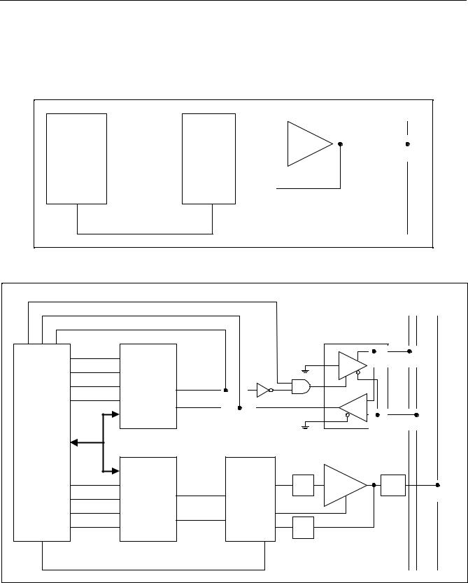
Introduction
The Intellon SSC P485 PL Transceiver IC is a highly integrated spread spectrum communication transceiver for implementing low-cost networking products. The SSC P485 contains a Spread Spectrum Carrierä (SSC) transceiver, signal conditioning circuitry, and a simple host interface. A minimum of external circuitry is required to connect the SSC P485 to the DC power line, twisted pair cable, or other communication medium.
The inherent reliability of SSC signaling technology provides substantial improvement in network and communication performance over other low-cost communication methods. The SSC P485 is the ideal basic communications element for a wide variety of low-cost networking applications.
SSC P485 Block Diagram
RST* |
|
|
|
|
|
ILD |
|
|
|
|
|
RO |
RX Interface Logic |
Data Decode |
Tracking & Data |
|
|
|
|
|
|||
|
Logic |
Extraction Logic |
|
|
|
|
|
|
|
||
WL |
|
|
|
|
C2 |
|
|
|
|
|
|
|
Summation |
Binary Shift |
Comp |
|
C1 |
|
|
|
|||
|
Encoder |
Register |
Amp |
SI |
|
|
|
||||
|
|
|
|
||
DI |
TX Interface Logic |
Waveform |
DAC |
Buf |
SO |
|
|
||||
|
Generator |
|
|||
|
|
|
|
|
|
4 MHz |
|
|
|
|
TS* |
|
|
|
TS Control |
||
XIN |
|
|
|
||
|
|
|
|
|
|
XOUT |
Clock Circuit |
|
|
|
|
July 1998 |
Revision 5 |
|
24000828 |
ADVANCE INFORMATION
SSC P485 PL Transceiver IC
Absolute Maximum Ratings (1)
Symbol |
Parameter |
Value |
Unit |
VDDMAX |
DC Supply Voltage |
-0.3 to 7.0 |
V |
VIN |
Input Voltage at any Pin |
VSS-0.3 to VDD+0.3 |
V |
TSTG |
Storage Temperature |
-65 to +150 |
°C |
TL |
Lead Temperature (Soldering, 10 seconds) |
300 |
°C |
Notes:
1. Absolute Maximum Ratings indicate limits beyond which damage to the device may occur.
Recommended Operating Conditions
Symbol |
Parameter |
Min |
Typical |
Max |
Unit |
VDD |
DC Supply Voltage |
4.5 |
5.0 |
5.5 |
V |
FOSC |
Oscillator Frequency |
|
12 ± 0.05% |
|
MHz |
TA |
Operating Temperature |
-40 |
+25 |
+85 |
°C |
|
Humidity (non-condensing) |
|
|
95 |
% |
Electrical Characteristics
Conditions: VDD = 4.5 to 5.5 V T= -40 to +85°C |
|
|
|
|
||
|
|
|
|
|
|
|
|
Symbol |
Parameter |
Min |
Typical |
Max |
Units |
|
VOH |
Minimum High-level Output Voltage |
2.4 |
|
|
V |
|
VOL |
Maximum Low-level Output Voltage (1) |
|
|
0.4 |
V |
|
VIH |
Minimum High-level Input Voltage |
2.0 |
|
|
V |
|
VIL |
Maximum Low-level Input Voltage |
|
|
0.8 |
V |
|
IIL |
Maximum Input Leakage Current |
|
|
±10 |
μA |
|
vSO |
SSC Signal Output Voltage (2) |
|
4 |
|
VP-P |
|
IDD |
Total Power Supply Current |
|
15 |
|
mA |
Notes:
1.TS* pin IOL = 4 mA, all other outputs IOL = 2 mA
2.ZL = 2K Ω || 10 pF
July 1998 |
2 |
Revision 5 |
|
|
24000828 |
ADVANCE INFORMATION

SSC P485 PL Transceiver IC
SSC P485 Pin Assignments
Pin |
Mnemonic |
Name |
Description |
1 |
4MHZ |
4 MHz Clock Out |
4 MHz clock output available for host microcontroller. |
2 |
NC |
No Connect |
|
3 |
VSSD |
Digital Ground |
Digital ground reference. |
4 |
XIN |
Crystal Input |
Connected to external crystal to excite the IC’s internal |
|
|
|
oscillator and digital clock. |
5 |
XOUT |
Crystal Output |
Connected to external crystal to excite the IC’s internal |
|
|
|
oscillator and digital clock. |
6 |
VDDD |
Digital Supply |
5.0 VDC ± 10% digital supply voltage with respect to |
|
|
|
VSSD. |
7 |
ILD |
Idle Line Detect |
Digital output, active high. Logic 1 state indicates 10 bit |
|
|
|
times of idle line, logic 0 indicates detection of carrier or |
|
|
|
non-idle line. |
8 |
DI |
Driver Input |
Digital input. After the preamble, a low on DI (SPACE) |
|
|
|
transmits a superior2 state on SO, a high on DI (MARK) |
|
|
|
transmits a superior1 state on SO. |
9 |
RO |
Receiver Output |
Digital output. After the preamble and assuming |
|
|
|
standard polarity: if superior1 state is detected on SI, |
|
|
|
RO will be high (MARK), if superior2 state is detected |
|
|
|
on SI, RO will be low (SPACE). |
10 |
WL |
Word Length |
Digital input. Logic 1 (default, internal pullup) selects |
|
|
|
10-bit frame (START, eight data bits, STOP), logic 0 |
|
|
|
selects 11-bit frame (START, nine data bits, STOP). |
11 |
TS* |
Tristate |
Active low digital output. Enables the external output |
|
|
|
amplifier when driven high. Tri-states the external |
|
|
|
output amplifier when driven low. |
12 |
RST* |
Reset |
Active low digital input. RST* asynchronously forces |
|
|
|
RO and ILD outputs to a high state and TS* to a low |
|
|
|
state. RST* can be asserted anytime during normal |
|
|
|
operation to force the reset state. RST* must be active |
|
|
|
(low) for 1 μsec after VDDD and VDDA stabilize and the |
|
|
|
crystal oscillator stabilizes to guarantee the internal |
|
|
|
reset state. See Figure 10. |
13 |
VSSA |
Analog Ground |
Analog ground reference. |
14 |
SO |
Signal Output |
Analog signal output. Tri-state enabled with internal |
|
|
|
signal. |
15 |
C2 |
Capacitor 2 |
Connection for 680pF capacitor to ground. |
16 |
C1 |
Capacitor 1 |
Connection for 680pF capacitor to ground. |
17 |
SI |
Signal Input |
Analog signal input. |
18 |
VDDA |
Analog Supply |
5.0 VDC ± 10% analog supply voltage with respect to |
|
|
|
VSSA. |
19 |
TP0 |
Test Point 0 |
Reserved pin for testing. |
20 |
VSSD |
Digital Ground |
Digital ground reference. |
July 1998 |
3 |
Revision 5 |
|
|
24000828 |
ADVANCE INFORMATION
SSC P485 PL Transceiver IC
SSC P485 Application Examples
The SSC P485 may be used in a wide variety of applications. A typical node connecting to the medium is shown in Figure 1. A gateway between an RS485 twisted pair network and a DC power line network is shown in Figure 2. A multi-point network application with gateways using the SSC P485 is illustrated in Figure 3. Figure 4 presents a host interface flow diagram showing the major steps necessary to transmit and receive messages using the P485 IC.
Single
W ire
|
W R |
DI |
|
SO |
output |
|
|
SSC P111 |
|
medium |
|
|
|
|
|
|
|
|
|
|
|||||||
|
|
|
|
Power Line Media |
|
|
|
||||||
Microprocessor |
|
|
|
|
filter |
|
|
|
coupler |
|
|
||
|
|
|
|
|
|
Interface |
|
|
|
||||
|
|
SSC P485 PL |
|
|
|
|
|
|
|
||||
based Control |
|
|
|
|
|
|
|
|
|
|
|
||
RD |
RO |
Transceiver |
|
|
|
|
|
|
|
|
|
||
Logic |
|
TS* |
|
|
|
|
|
||||||
|
|
|
|
|
|
|
|
|
|
||||
|
|
|
|
|
|
|
|
|
|
|
|||
|
|
|
|
SI |
|
|
|
|
|
|
|
|
|
|
|
|
|
input |
|
|
|
|
|
|
|
|
|
|
|
|
|
|
filter |
|
|
|
|
|
|
|
|
|
|
|
|
|
|
|
|
|
|
|
|
|
|
ILD
Figure 1. SSC P485 Typical Node
Transmit Enable #1 |
|
|
|
Twisted |
Single |
RXD #1 |
Pair |
Wire |
TXD #1
|
|
|
|
|
|
RS-485 Transceiver |
|
|
|
|
|
|
|
|
A |
TXRDY #1 |
|
|
|
|
|
|
|
|
|
|
|
|
|
D |
|
RXRDY #1 |
|
|
|
|
|
|
|
RD #1 |
UART |
TXD #1 |
|
|
DE |
|
|
|
|
|
|
|
|||
WR #1 |
|
|
|
|
|
+ |
|
|
|
RXD #1 |
|
|
|
||
|
|
|
|
R |
|
||
|
|
|
|
|
|
- |
B |
|
|
|
|
|
|
|
|
|
|
|
|
|
|
RE* |
|
Microprocessor |
|
|
|
|
|
|
|
DATA 0-7 |
|
|
|
|
|
|
|
based Control |
|
|
|
|
|
|
|
Logic |
|
|
|
|
|
|
|
RD #2 |
|
|
|
SO |
output |
SSC P111 |
medium |
|
|
|
Power Line Media |
||||
|
|
|
|
|
filter |
coupler |
|
|
|
TXD #2 |
|
|
Interface |
||
WR #2 |
|
DI |
SSC P485 PL |
|
|
||
UART |
|
|
|
|
|||
|
|
|
|
|
|||
|
|
|
Transceiver |
|
|
|
|
|
|
|
|
|
|
|
|
TXRDY #2 |
|
|
|
|
|
TS* |
|
|
|
RXD #2 |
RO |
|
|
|
|
RXRDY #2 |
|
|
|
SI |
input |
|
|
|
|
|
|
|
filter |
|
|
|
|
|
|
ILD |
|
|
|
ILD |
|
|
|
|
|
|
|
Figure 2. SSC P485 Gateway
July 1998 |
4 |
Revision 5 |
|
|
24000828 |
ADVANCE INFORMATION
SSC P485 PL Transceiver IC
|
|
|
|
|
|
|
P111 |
|
DC power line |
P111 |
|
|
|
|
|
|||
host |
|
|
|
P485 |
|
|
IC |
|
|
|
IC |
|
|
P485 |
|
|
|
host |
|
|
|
|
|
|
|
|
|
|
|
|
|
|
|
||||
micro |
|
|
|
|
|
|
|
|
|
|
|
|
|
|
|
micro |
||
|
|
|
IC |
|
|
|
|
|
|
|
|
|
IC |
|
|
|
||
|
|
|
|
|
|
|
|
|
|
|
|
|
|
|
|
|
||
|
|
|
|
|
|
|
|
|
|
|
|
|
|
|
|
|
|
|
|
|
|
|
|
|
|
|
|
|
|
|
|
|
|
|
|
|
|
|
|
|
|
|
|
|
|
|
|
|
gateway |
|
|
|
|
|
|
|
|
|
|
gateway |
|
|
|
|
|
|
|
|
|||||||||||||||||||
|
|
|
|
|
|
|
|
|
|
|
|
|
|
|
|
|
|
|
|
|
|
|
P111 |
|
|
P111 |
|
|
|
|
|
|
|
|
|
|
|
|
|
|
|
|
|
||||||
|
|
|
|
|
|
|
|
|
|
|
|
|
|
|
|
|
|
|
|
|
|
|
|
|
|
|
|
|
|
|
|
|
|
|
|
|
|
|
|
|
|
||||||||
RS485 |
|
|
|
|
|
|
|
|
|
|
|
|
|
|
|
|
|
|
|
|
|
|
|
|
|
|
|
|
|
|
|
RS485 |
|||||||||||||||||
|
|
|
|
|
gate |
|
|
|
|
|
|
|
|
|
|
|
|
IC |
|
|
|
IC |
|
|
|
|
|
|
|
|
|
|
|
gate |
|
|
|
|
|
||||||||||
|
IC |
|
|
|
|
|
|
|
|
|
|
P485 |
|
|
|
|
|
|
|
|
|
|
|
|
|
|
|
P485 |
|
|
|
|
|
|
|
|
|
|
|
IC |
|||||||||
|
|
|
|
|
|
way |
|
|
|
|
|
|
|
|
|
|
|
|
|
|
|
|
|
|
|
|
|
|
|
|
|
way |
|
|
|
|
|
|
|||||||||||
|
|
|
|
|
|
|
|
|
|
|
|
|
|
|
|
|
|
|
|
|
|
|
|
|
|
|
|
|
|
|
|
|
|
|
|
||||||||||||||
|
|
|
|
|
|
|
|
|
micro |
|
|
|
|
|
IC |
|
|
|
|
|
|
|
|
|
|
|
|
|
|
|
IC |
|
|
|
|
|
micro |
|
|
|
|
|
|
|
|
||||
|
|
|
|
|
|
|
|
|
|
|
|
|
|
|
|
|
|
|
|
|
|
||||||||||||||||||||||||||||
|
|
|
|
|
|
|
|
|
|
|
|
|
|
|
|
|
|
|
|
|
|
|
|
|
|
|
|
|
|
|
|
|
|
|
|
|
|
|
|
|
|
|
|
|
|
|
|
|
|
|
|
|
|
|
|
|
|
|
|
|
|
|
|
|
|
|
|
|
|
|
|
|
|
|
|
|
|
|
|
|
|
|
|
|
|
|
|
|
|
|
|
|
|
|
|
|
|
|
|
|
|
|
|
|
|
|
|
|
|
|
|
|
|
|
|
|
|
|
|
|
|
|
|
|
|
|
|
|
|
|
|
|
|
|
|
|
|
|
|
|
|
|
|
|
|
|
|
|
|
|
|
|
|
|
|
|
|
|
|
|
|
|
|
|
|
|
|
|
|
|
|
|
|
|
|
|
|
|
|
|
|
|
|
|
|
|
|
|
|
|
|
|
|
|
|
|
|
|
|
|
|
|
|
|
|
|
|
|
|
|
|
|
|
|
|
|
|
|
|
|
|
|
|
|
|
|
|
|
|
|
|
|
|
|
|
|
|
|
|
|
|
|
|
|
|
|
|
|
|
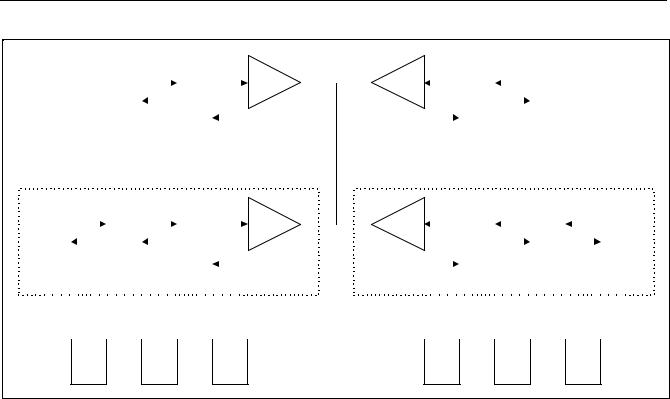
RS485 |
RS485 |
RS485 |
RS485 |
RS485 |
RS485 |
device |
device |
device |
device |
device |
device |
Figure 3. SSC P485 Multi-point Network Application
July 1998 |
5 |
Revision 5 |
|
|
24000828 |
ADVANCE INFORMATION

SSC P485 PL Transceiver IC
|
Entry |
|
|
|
|
|
No |
|
|
|
|
|
|
|
|
|
|
|
message to |
|
|
|
write 1st character to |
|
UART indicates |
|
|
Yes |
ILD==logic 1? |
Yes |
|
receive character |
|
||
|
transmit? |
UART |
|
|
||||
|
|
|
|
|
available? |
|
||
|
|
|
|
|
|
|
|
|
|
|
No |
|
|
|
|
Yes |
|
|
|
|
|
|
|
|
|
|
|
|
|
|
|
|
|
read character from |
|
|
|
|
|
|
|
|
UART |
|
|
|
|
|
|
transmitted last |
|
character |
|
|
|
|
Yes |
|
Yes |
transmitted==character |
|
|
|
|
|
|
character? |
|
|||
|
|
|
|
|
|
received? |
|
|
|
|
|
|
|
|
|
|
|
|
|
|
|
|
No |
|
|
|
|
|
|
|
write next character to |
|
|
|
|
|
|
|
|
|
UART |
|
|
|
|
No |
|
|
|
|
Yes |
|
|
|
|
|
|
|
|
|
|
|
|
|
|
No |
|
|
|
No |
|
|
|
|
|
|
UART indicates |
|
|
|
|
|
|
|
|
|
|
|
|
|
|
|
|
|
transmit buffer |
|
|
|
|
|
|
|
|
available? |
|
|
|
|
No |
|
|
|
|
|
|
|
|
|
|
ILD==logic 1? |
|
|
|
|
|
|
|
|
Yes |
|
|
|
store character in |
|
|
|
|
|
|
|
|
|
|
|
|
|
|
|
|
|
message |
|
|
|
|
message has been |
|
|
|
|
|
|
|
|
transmitted |
|
|
|
|
|
|
UART indicates |
|
|
|
read character from |
Yes |
UART indicates |
|
No |
receive character |
|
Yes |
|
receive character |
|
||
|
|
UART |
|
|||||
|
available? |
|
|
|
|
available? |
|
|
|
|
|
|
|
|
|
||
|
|
|
|
|
|
|
No |
No |
|
|
|
|
|
|
|
1-1/2 char times |
|
|
|
|
|
|
process message |
Yes |
of quiet since last |
|
|
|
|
|
|
|
|
character? |
|
Figure 4. Host Interface Flow Diagram
July 1998 |
6 |
Revision 5 |
|
|
24000828 |
ADVANCE INFORMATION
 Loading...