


*Other brands and names are the property of their respective owners.
Information in this document is provided in connection with Intel products. Intel assumes no liability whatsoever, including infringement of any patent or
copyright, for sale and use of Intel products except as provided in Intel’s Terms and Conditions of Sale for such products. Intel retains the right to make
changes to these specifications at any time, without notice. Microcomputer Products may have minor variations to this specification known as errata.
November 1995COPYRIGHT©INTEL CORPORATION, 1995 Order Number: 290406-007
1-MBIT (128K x 8)
BOOT BLOCK FLASH MEMORY
28F001BX-T/28F001BX-B/28F001BN-T/28F001BN-B
Y
High-Integration Blocked Architecture
Ð One 8 KB Boot Block w/Lock Out
Ð Two 4 KB Parameter Blocks
Ð One 112 KB Main Block
Y
100,000 Erase/Program Cycles Per
Block
Y
Simplified Program and Erase
Ð Automated Algorithms via On-Chip
Write State Machine (WSM)
Y
SRAM-Compatible Write Interface
Y
Deep Power-Down Mode
Ð 0.05 mAI
CC
Typical
Ð 0.8 mAI
PP
Typical
Y
12.0Vg5% V
PP
Y
High-Performance Read
Ð 70/75 ns, 90 ns, 120 ns, 150 ns
Maximum Access Time
Ð 5.0V
g
10% V
CC
Y
Hardware Data Protection Feature
Ð Erase/Write Lockout during Power
Transitions
Y
Advanced Packaging, JEDEC Pinouts
Ð 32-Pin PDIP
Ð 32-Lead PLCC, TSOP
Y
ETOXTMII Nonvolatile Flash
Technology
Ð EPROM-Compatible Process Base
Ð High-Volume Manufacturing
Experience
Y
Extended Temperature Options
Intel’s 28F001BX-B and 28F001BX-T combine the cost-effectiveness of Intel standard flash memory with
features that simplify write and allow block erase. These devices aid the system designer by combining the
functions of several components into one, making boot block flash an innovative alternative to EPROM and
EEPROM or battery-backed static RAM. Many new and existing designs can take advantage of the
28F001BX’s integration of blocked architecture, automated electrical reprogramming, and standard processor
interface.
The 28F001BX-B and 28F001BX-T are 1,048,576 bit nonvolatile memories organized as 131,072 bytes of
8 bits. They are offered in 32-pin plastic DIP, 32-lead PLCC and 32-lead TSOP packages. Pin assignment
conform to JEDEC standards for byte-wide EPROMs. These devices use an integrated command port and
state machine for simplified block erasure and byte reprogramming. The 28F001BX-T’s block locations provide compatibility with microprocessors and microcontrollers that boot from high memory, such as Intel’s
MCS
É
-186 family, 80286, i386TM, i486TM, i860TMand 80960CA. With exactly the same memory segmentation,
the 28F001BX-B memory map is tailored for microprocessors and microcontrollers that boot from low memory,
such as Intel’s MCS-51, MCS-196, 80960KX and 80960SX families. All other features are identical, and unless
otherwise noted, the term 28F001BX can refer to either device throughout the remainder of this document.
The boot block section includes a reprogramming write lock out feature to guarantee data integrity. It is
designed to contain secure code which will bring up the system minimally and download code to the other
locations of the 28F001BX. Intel’s 28F001BX employs advanced CMOS circuitry for systems requiring highperformance access speeds, low power consumption, and immunity to noise. Its access time provides
no-WAIT-state performance for a wide range of microprocessors and microcontrollers. A deep-powerdown
mode lowers power consumption to 0.25 mW typical through V
CC
, crucial in laptop computer, handheld instru-
mentation and other low-power applications. The RP
Ý
power control input also provides absolute data protec-
tion during system powerup or power loss.
Manufactured on Intel’s ETOX process base, the 28F001BX builds on years of EPROM experience to yield the
highest levels of quality, reliability, and cost-effectiveness.
NOTE: The 28F001BN is equivalent to the 28F001BX.
28F001BX-T/28F001BX-B
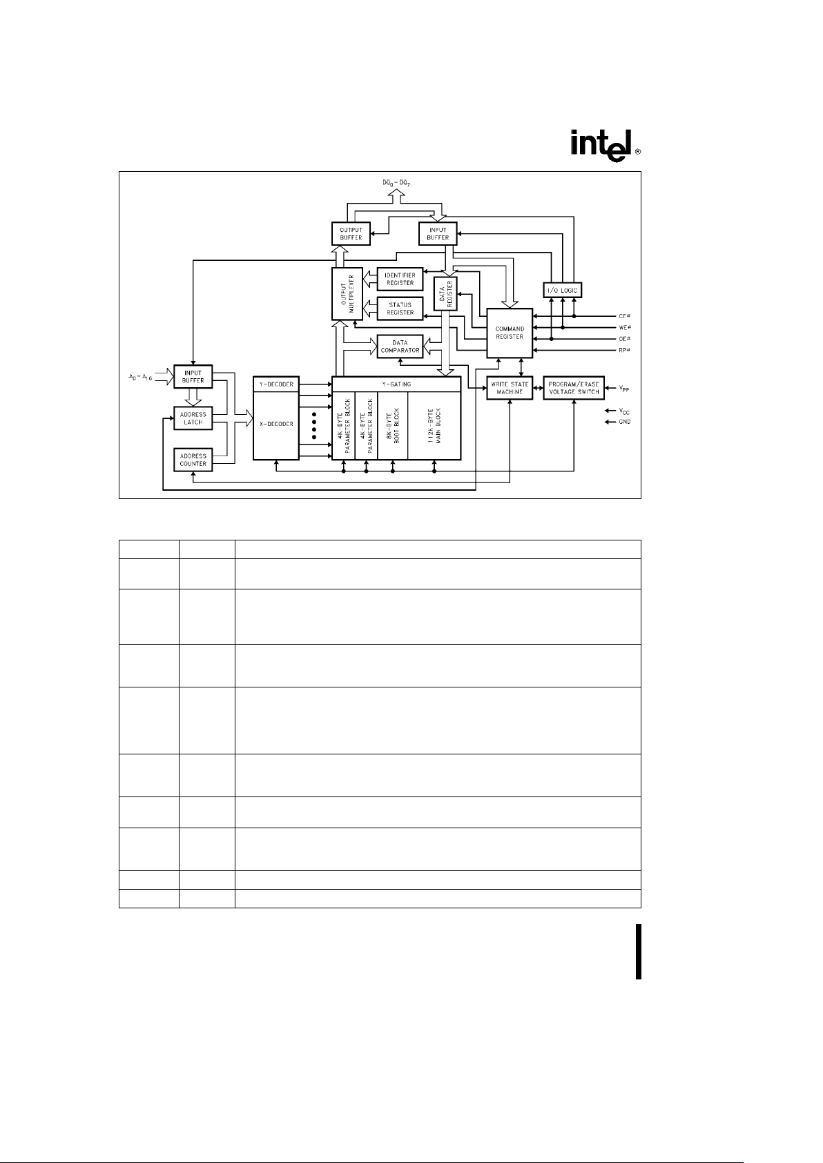
290406– 1
Figure 1. 28F001BX Block Diagram
Table 1. Pin Description
Symbol Type Name and Function
A0–A
16
INPUT ADDRESS INPUTS for memory addresses. Addresses are internally latched during
a write cycle.
DQ0–DQ7INPUT/ DATA INPUTS/OUTPUTS: Inputs data and commands during memory write
cycles; outputs data during memory, Status Register and Identifier read cycles. The
OUTPUT
data pins are active high and float to tri-state off when the chip is deselected or the
outputs are disabled. Data is internally latched during a write cycle.
CE
Ý
INPUT CHIP ENABLE: Activates the device’s control logic, input buffers, decoders and
sense amplifiers. CE
Ý
is active low; CEÝhigh deselects the memory device and
reduces power consumption to standby levels.
RP
Ý
INPUT POWERDOWN: Puts the device in deep powerdown mode. RPÝis active low;
RP
Ý
high gates normal operation. RP
Ý
e
VHHallows programming of the boot
block. RP
Ý
also locks out erase or write operations when active low, providing data
protection during power transitions. RPÝactive resets internal automation. Exit
from deep powerdown sets device to Read Array mode.
OE
Ý
INPUT OUTPUT ENABLE: Gates the device’s outputs through the data buffers during a
read cycle. OE
Ý
is active low. OE
Ý
e
VHH(pulsed) allows programming of the
boot block.
WE
Ý
INPUT WRITE ENABLE: Controls writes to the Command Register and array blocks. WE
Ý
is active low. Addresses and data are latched on the rising edge of the WEÝpulse.
V
PP
ERASE/PROGRAM POWER SUPPLY for erasing blocks of the array or
programming bytes of each block. Note: With V
PP
k
V
PPL
max, memory contents
cannot be altered.
V
CC
DEVICE POWER SUPPLY: (5Vg10%)
GND GROUND
2
28F001BX-T/28F001BX-B
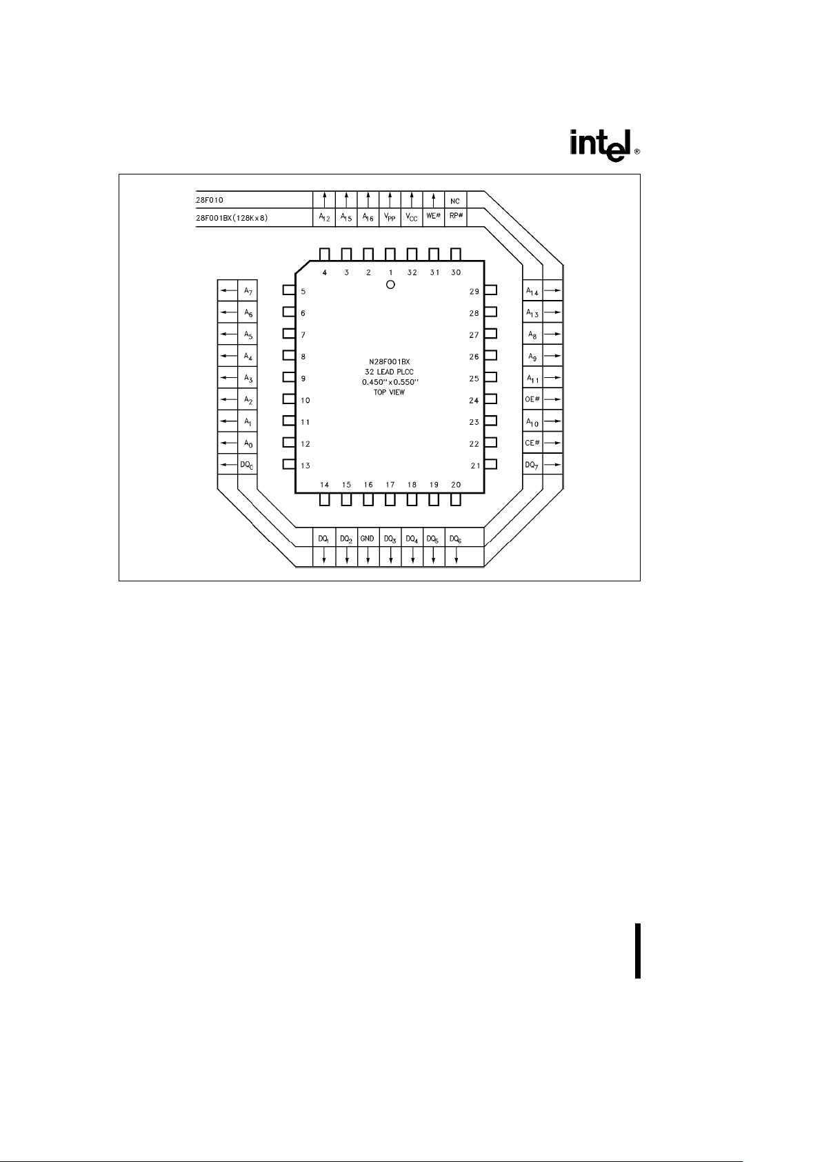
28F010
V
PP
A
16
A
15
A
12
A
7
A
6
A
5
A
4
A
3
A
2
A
1
A
0
DQ
0
DQ
1
DQ
2
GND
290406– 2
28F010
V
CC
WE
Ý
NC
A
14
A
13
A
8
A
9
A
11
OE
Ý
A
10
CE
Ý
DQ
7
DQ
6
DQ
5
DQ
4
DQ
3
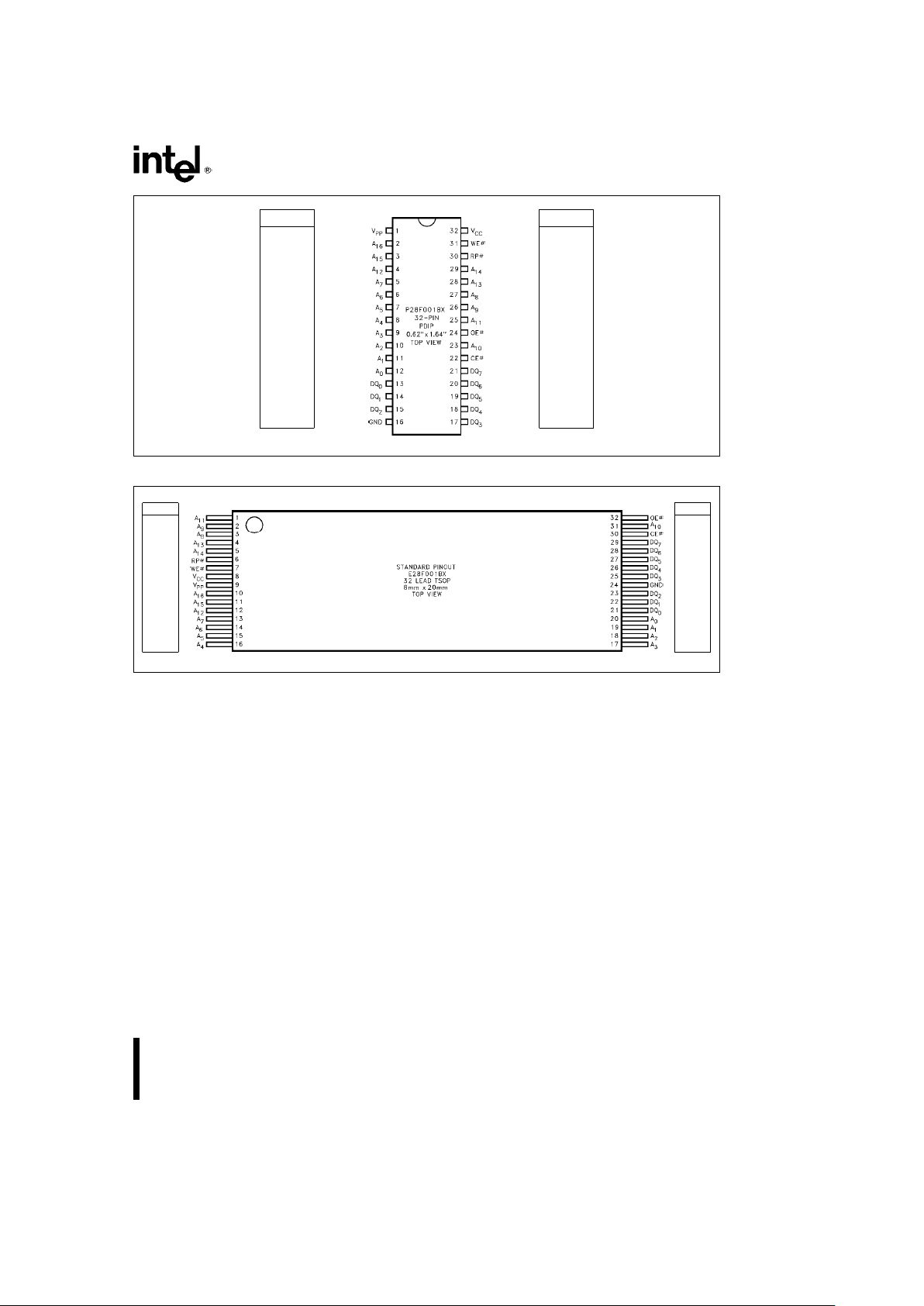
Figure 2. DIP Pin Configuration
28F010
A
11
A
9
A
8
A
13
A
14
NC
WE
Ý
V
CC
V
PP
A
16
A
15
A
12
A
7
A
6
A
5
A
4
290406– 3
28F010
OE
Ý
A
10
CE
Ý
DQ
7
DQ
6
DQ
5
DQ
4
DQ
3
GND
DQ
2
DQ
1
DQ
0
A
0
A
1
A
2
A
3
Figure 3. TSOP Lead Configuration
3
28F001BX-T/28F001BX-B
290406– 4
Figure 4. PLCC Lead Configuration
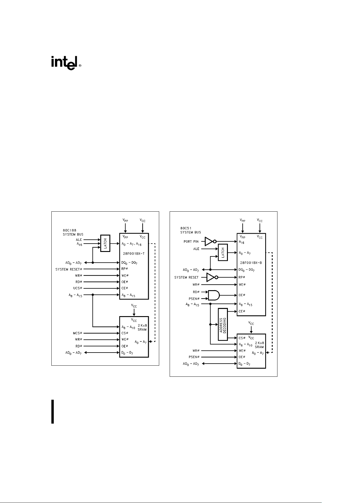
APPLICATIONS
The 28F001BX flash ‘boot block’ memory augments
the non-volatility, in-system electrical erasure and
reprogrammability of Intel’s standard flash memory
by offering four separately erasable blocks and integrating a state machine to control erase and program functions. The specialized blocking architecture and automated programming of the 28F001BX
provide a full-function, non-volatile flash memory
ideal for a wide range of applications, including PC
boot/BIOS memory, minimum-chip embedded program memory and parametric data storage. The
28F001BX combines the safety of a hardware-protected 8-KByte boot block with the flexibility of three
separately reprogrammable blocks (two 4-KByte parameter blocks and one 112-KByte code block) into
one versatile, cost-effective flash memory. Additionally, reprogramming one block does not affect code
stored in another block, ensuring data integrity.
The flexibility of flash memory reduces costs
throughout the life cycle of a design. During the early
stages of a system’s life, flash memory reduces prototype development and testing time, allowing the
system designer to modify in-system software electrically versus manual removal of components. During production, flash memory provides flexible firmware for just-in-time configuration, reducing system
inventory and eliminating unnecessary handling and
less reliable socketed connections. Late in the life
cycle, when software updates or code ‘‘bugs’’ are
often unpredictable and costly, flash memory reduces update costs by allowing the manufacturers to
send floppy updates versus a technician. Alternatively, remote updates over a communication link are
possible at speeds up to 9600 baud due to flash
memory’s fast programming time.
4
28F001BX-T/28F001BX-B
Reprogrammable environments, such as the personal computer, are ideal applications for the
28F001BX. The internal state machine provides
SRAM-like timings for program and erasure, using
the Command and Status Registers. The blocking
scheme allows BIOS update in the main and parameter blocks, while still providing recovery code in the
boot block in the unlikely event a power failure occurs during an update, or where BIOS code is corrupted. Parameter blocks also provide convenient
configuration storage, backing up SRAM and battery
configurations. EISA systems, for example, can
store hardware configurations in a flash parameter
block, reducing system SRAM.
Laptop BIOSs are becoming increasingly complex
with the addition of power management software
and extended system setup screens. BIOS code
complexity increases the potential for code updates
after the sale, but the compactness of laptop designs makes hardware updates very costly. Boot
block flash memory provides an inexpensive update
solution for laptops, while reducing laptop obsolescence. For portable PCs and hand-held equipment,
the deep powerdown mode dramatically lowers sys-
tem power requirements during periods of slow operation or sleep modes.
The 28F001BX gives the embedded system designer several desired features. The internal state machine reduces the size of external code dedicated to
the erase and program algorithms, as well as freeing
the microcontroller or microprocessor to respond to
other system requests during program and erasure.
The four blocks allow logical segmentation of the
entire embedded software: the 8-KByte block for the
boot code, the 112-KByte block for the main program code and the two 4-KByte blocks for updatable
parametric data storage, diagnostic messages and
data, or extensions of either the boot code or program code. The boot block is hardware protected
against unauthorized write or erase of its vital code
in the field. Further, the powerdown mode also locks
out erase or write operations, providing absolute
data protection during system powerup or power
loss. This hardware protection provides obvious advantages for safety related applications such as
transportation, military, and medical. The 28F001BX
is well suited for minimum-chip embedded applications ranging from communications to automotive.
290406– 5
Figure 5. 28F001BX-T in a 80C188 System
290406– 6
Figure 6. 28F001BX-B in a 80C51 System
5

28F001BX-T/28F001BX-B
PRINCIPLES OF OPERATION
The 28F001BX introduces on-chip write automation
to manage write and erase functions. The write state
machine allows for 100% TTL-level control inputs,
fixed power supplies during erasure and programming, minimal processor overhead with RAM-like
write timings, and maximum EPROM compatiblity.
After initial device powerup, or after return from
deep powerdown mode (see Bus Operations), the
28F001BX functions as a read-only memory. Manipulation of external memory-control pins yield standard EPROM read, standby, output disable or Intelligent Identifier operations. Both Status Register and
Intelligent Identifiers can be accessed through the
Command Register when V
PP
e
V
PPL
.
This same subset of operations is also available
when high voltage is applied to the V
PP
pin. In addi-
tion, high voltage on V
PP
enables successful erasure
and programming of the device. All functions associated with altering memory contentsÐprogram,
erase, status, and inteligent IdentifierÐare accessed
via the Command Register and verified through the
Status Register.
Commands are written using standard microprocessor write timings. Register contents serve as input to
the WSM, which controls the erase and programming circuitry. Write cycles also internally latch addresses and data needed for programming or erase
operations. With the appropriate command written to
the register, standard microprocessor read timings
output array data, access the intelligent identifier
codes, or output program and erase status for verification.
Interface software to initiate and poll progress of internal program and erase can be stored in any of the
28F001BX blocks. This code is copied to, and executed from, system RAM during actual flash memory
update. After successful completion of program
and/or erase, code execution out of the 28F001BX
is again possible via the Read Array command.
Erase suspend/resume capability allows system
software to suspend block erase and read data/execute code from any other block.
Command Register and Write
Automation
An on-chip state machine controls block erase and
byte program, freeing the system processor for other
tasks. After receiving the erase setup and erase
confirm commands, the state machine controls
block pre-conditioning and erase, returning progress
via the Status Register. Programming is similarly
controlled, after destination address and expected
data are supplied. The program algorithm of past Intel Flash Memories is now regulated by the state
machine, including program pulse repetition where
required and internal verification and margining of
data.
Data Protection
Depending on the application, the system designer
may choose to make the V
PP
power supply switchable (available only when memory updates are required) or hardwired to V
PPH
. When V
PP
e
V
PPL
,
memory contents cannot be altered. The 28F001BX
Command Register architecture provides protection
from unwanted program or erase operations even
when high voltage is applied to V
PP
. Additionally, all
functions are disabled whenever V
CC
is below the
write lockout voltage V
LKO
, or when RPÝis at VIL.
The 28F001BX accommodates either design practice and encourages optimization of the processormemory interface.
The two-step program/erase write sequence to the
Command Register provides additional software
write protection.
1FFFF
8-KByte BOOT BLOCK
1DFFF
1E000
4-KByte PARAMETER BLOCK
1CFFF
1D000
4-KByte PARAMETER BLOCK
1BFFF
1C000
112-KByte MAIN BLOCK
00000
Figure 7. 28F001BX-T Memory Map
1FFFF
112-KByte MAIN BLOCK
03FFF
04000
4-KByte PARAMETER BLOCK
02FFF
03000
4-KByte PARAMETER BLOCK
01FFF
02000
8-KByte BOOT BLOCK
00000
Figure 8. 28F001BX-B Memory Map
6

28F001BX-T/28F001BX-B
BUS OPERATION
Flash memory reads, erases and writes in-system
via the local CPU. All bus cycles to or from the flash
memory conform to standard microprocessor bus
cycles.
Read
The 28F001BX has three read modes. The memory
can be read from any of its blocks, and information
can be read from the Intelligent Identifier or the
Status Register. V
PP
can be at either V
PPL
or V
PPH
.
The first task is to write the appropriate read mode
command to the Command Register (array, Intelligent Identifier, or Status Register). The 28F001BX
automatically resets to Read Array mode upon initial
device powerup or after exit from deep powerdown.
The 28F001BX has four control pins, two of which
must be logically active to obtain data at the outputs.
Chip Enable (CE
Ý
) is the device selection control,
and when active enables the selected memory device. Output Enable (OE
Ý
) is the data input/output
(DQ
0
–DQ7) direction control, and when active
drives data from the selected memory onto the I/O
bus. RP
Ý
and WEÝmust also be at VIH. Figure 12
illustrates read bus cycle waveforms.
Output Disable
With OEÝat a logic-high level (VIH), the device outputs are disabled. Output pins (DQ
0
–DQ7) are
placed in a high-impedance state.
Standby
CEÝat a logic-high level (VIH) places the 28F001BX
in standby mode. Standby operation disables much
of the 28F001BX’s circuitry and substantially reduces device power consumption. The outputs (DQ
0
–
DQ
7
) are placed in a high-impedance state indepen-
dent of the status of OE
Ý
. If the 28F001BX is deselected during erase or program, the device will
continue functioning and consuming normal active
power until the operation is completed.
Deep Power-Down
The 28F001BX offers a 0.25 mWVCCpower-down
feature, entered when RP
Ý
is at VIL. During read
modes, RP
Ý
low deselects the memory, places output drivers in a high-impedance state and turns off
all internal circuits. The 28F001BX requires time
t
PHQV
(see AC Characteristics-Read Only Operations) after return from power-down until initial memory access outputs are valid. After this wakeup interval, normal operation is restored. The Command
Register is reset to Read Array, and the Status Register is cleared to value 80H, upon return to normal
operation.
During erase or program modes, RP
Ý
low will abort
either operation. Memory contents of the block being altered are no longer valid as the data will be
partially programmed or erased. Time t
PHWL
after
RP
Ý
goes to logic-high (VIH) is required before an-
other command can be written.
Table 2. 28F001BX Bus Operations
Mode Notes RPÝCEÝOEÝWEÝA9A0V
PP
DQ
0–7
Read 1, 2, 3 V
IH
V
IL
V
IL
V
IH
XX X D
OUT
Output Disable 2 V
IH
V
IL
V
IH
V
IH
X X X High Z
Standby 2 V
IH
V
IH
X X X X X High Z
Deep Power Down 2 V
IL
X X X X X X High Z
Intelligent Identifier (Mfr) 2, 3, 4 V
IH
V
IL
V
IL
V
IH
VIDV
IL
X 89H
Intelligent Identifier (Device) 2, 3, 4, 5 V
IH
V
IL
V
IL
V
IH
VIDV
IH
X 94H, 95H
Write 2, 6, 7, 8 V
IH
V
IL
V
IH
V
IL
XX X D
IN
NOTES:
1. Refer to DC Characteristics. When V
PP
e
V
PPL
, memory contents can be read but not programmed or erased.
2. X can be V
IL
or VIHfor control pins and addresses, and V
PPL
or V
PPH
for VPP.
3. See DC Characteristics for V
PPL,VPPH,VHH
and VIDvoltages.
4. Manufacturer and device codes may also be accessed via a Command Register write sequence. Refer to Table 3. A
1–A8
,
A
10–A16
e
VIL.
5. Device ID
e
94H for the 28F001BX-T and 95H for the 28F001BX-B.
6. Command writes involving block erase or byte program are successfully executed only when V
PP
e
V
PPH
.
7. Refer to Table 3 for valid D
IN
during a write operation.
8. Program or erase the boot block by holding RP
Ý
at VHHor toggling OEÝto VHH. See AC Waveforms for program/erase
operations.
7

28F001BX-T/28F001BX-B
The use of RPÝduring system reset is important
with automated write/erase devices. When the system comes out of reset it expects to read from the
flash memory. Automated flash memories provide
status information when accessed during write/
erase modes. If a CPU reset occurs with no flash
memory reset, proper CPU initialization would not
occur because the flash memory would be providing
the status information instead of array data. Intel’s
Flash Memories allow proper CPU initialization following a system reset through the use of the RP
Ý
input. In this application RPÝis controlled by the
same RESET
Ý
signal that resets the system CPU.
Intelligent Identifier Operation
The Intelligent Identifier operation outputs the manufacturer code, 89H; and the device code, 94H for the
28F001BX-T and 95H for the 28F001BX-B. Programming equipment or the system CPU can then
automatically match the device with its proper erase
and programming algorithms.
PROGRAMMING EQUIPMENT
CE
Ý
and OEÝat a logic low level (VIL), with A9at
high voltage V
ID
(see DC Characteristics) activates
this operation. Data read from locations 00000H and
00001H represent the manufacturer’s code and the
device code respectively.
IN-SYSTEM PROGRAMMING
The manufacturer- and device-codes can also be
read via the Command Register. Following a write of
90H to the Command Register, a read from address
location 00000H outputs the manufacturer code
(89H). A read from address 00001H outputs the device code (94H for the 28F001BX-T and 95H for the
28F001BX-B). It is not necessary to have high voltage applied to V
PP
to read the Intelligent Identifiers
from the Command Register.
Write
Writes to the Command Register allow read of device data and Intelligent Identifiers. They also control inspection and clearing of the Status Register.
Additionally, when V
PP
e
V
PPH
, the Command Register controls device erasure and programming. The
contents of the register serve as input to the internal
state machine.
The Command Register itself does not occupy an
addressable memory location. The register is a latch
used to store the command and address and data
information needed to execute the command. Erase
Setup and Erase Confirm commands require both
appropriate command data and an address within
the block to be erased. The Program Setup Command requires both appropriate command data and
the address of the location to be programmed, while
the Program command consists of the data to be
written and the address of the location to be programmed.
The Command Register is written by bringing WE
Ý
to a logic-low level (VIL) while CEÝis low. Addresses and data are latched on the rising edge of WE
Ý
.
Standard microprocessor write timings are used.
Refer to AC Write Characteristics and the AC Waveform for Write Operations, Figure 13, for specific timing parameters.
COMMAND DEFINITIONS
When V
PPL
is applied to the VPPpin, read operations from the Status Register, intelligent identifiers,
or array blocks are enabled. Placing V
PPH
on V
PP
enables successful program and erase operations
as well.
Device operations are selected by writing specific
commands into the Command Register. Table 3 defines these 28F001BX commands.
Read Array Command
Upon initial device powerup and after exit from
deep-powerdown mode, the 28F001BX defaults to
Read Array mode. This operation is also initiated by
writing FFH into the Command Register. Microprocessor read cycles retrieve array data. The device remains enabled for reads until the Command Register contents are altered. Once the internal write
state machine has started an erase or program operation, the device will not recognize the Read Array
command, until the WSM has completed its operation. The Read Array command is functional when
V
PP
e
V
PPL
or V
PPH
.
Intelligent Identifier Command for
In-System Programming
The 28F001BX contains an Intelligent Identifier operation to supplement traditional PROM-programming methodology. The operation is initiated by writing 90H into the Command Register. Following the
command write, a read cycle from address 00000H
retrieves the manufacturer code of 89H. A read cycle from address 00001H returns the device code of
94H (28F001BX-T) or 95H (28F001BX-B). To terminate the operation, it is necessary to write another
valid command into the register. Like the Read Array
command, the Intelligent Identifier command is functional when V
PP
e
V
PPL
or V
PPH
.
8
28F001BX-T/28F001BX-B
Table 3. 28F001BX Command Definitions
Command Cycles
Req’d
Bus
Notes
First Bus Cycle Second Bus Cycle
Operation Address Data Operation Address Data
Read Array/Reset 1 1 Write X FFH
Intelligent Identifier 3 2, 3, 4 Write X 90H Read IA IID
Read Status Register 2 3 Write X 70H Read X SRD
Clear Status Register 1 Write X 50H
Erase Setup/Erase Confirm 2 2 Write BA 20H Write BA D0H
Erase Suspend/Erase Resume 2 Write X B0H Write X D0H
Program Setup/Program 2 2, 3 Write PA 40H Write PA PD
NOTES:
1. Bus operations are defined in Table 2.
2. IA
e
Identifier Address: 00H for manufacturer code, 01H for device code.
BA
e
Address within the block being erased.
PA
e
Address of memory location to be programmed.
3. SRD
e
Data read from Status Register. See Table 4 for a description of the Status Register bits.
PD
e
Data to be programmed at location PA. Data is latched on the rising edge of WEÝ.
IID
e
Data read from Intelligent Identifiers.
4. Following the Intelligent Identifier command, two read operations access manufacture and device codes.
5. Commands other than those shown above are reserved by Intel for future device implementations and should not be
used.
Read Status Register Command
The 28F001BX contains a Status Register which
may be read to determine when a program or erase
operation is complete, and whether that operation
completed successfully. The Status Register may be
read at any time by writing the Read Status Register
command (70H) to the Command Register. After
writing this command, all subsequent read operations output data from the Status Register, until another valid command is written to the Command
Register. The contents of the Status Register are
latched on the falling edge of OE
Ý
or CEÝ, which-
ever occurs last in the read cycle. OE
Ý
or CE
Ý
must be toggled to VIHbefore further reads to update the Status Register latch. The Read Status
Register command functions when V
PP
e
V
PPL
or
V
PPH
.
Clear Status Register Command
The Erase Status and Program Status bits are set to
‘‘1’’ by the Write State Machine and can only be
reset by the Clear Status Register command. These
bits indicate various failure conditions (see Table 4).
By allowing system software to control the resetting
of these bits, several operations may be performed
(such as cumulatively programming several bytes or
erasing multiple blocks in sequence). The Status
Register may then be polled to determine if an error
occurred during that series. This adds flexibility to
the way the device may be used.
Additionally, the V
PP
Status bit (SR.3), when set to
‘‘1’’, MUST be reset by system software before further byte programs or block erases are attempted.
To clear the Status Register, the Clear Status Register command (50H) is written to the Command Register. The Clear Status Register command is functional when V
PP
e
V
PPL
or V
PPH
.
9

28F001BX-T/28F001BX-B
Table 4. 28F001BX Status Register Definitions
WSMS ESS ES PS VPPS R R R
76543210
SR.7eWRITE STATE MACHINE STATUS
1
e
Ready
0
e
Busy
SR.6
e
ERASE SUSPEND STATUS
1
e
Erase Suspended
0
e
Erase In Progress/Completed
SR.5
e
ERASE STATUS
1
e
Error in Block Erasure
0
e
Successful Block Erase
SR.4
e
PROGRAM STATUS
1
e
Error in Byte Program
0
e
Successful Byte Program
SR.3
e
VPPSTATUS
1
e
VPPLow Detect; Operation Abort
0
e
VPPOK
SR.2–SR.0
e
RESERVED FOR FUTURE ENHANCEMENTS
These bits are reserved for future use and should be
masked out when polling the Status Register.
NOTES:
The Write State Machine Status Bit must first be checked
to determine program or erase completion, before the
Program or Erase Status bits are checked for success.
If the Program AND Erase Status bits are set to ‘‘1s’’ during an erase attempt, an improper command sequence
was entered. Attempt the operation again.
If V
PP
low status is detected, the Status Register must be
cleared before another program or erase operation is attempted.
The V
PP
Status bit, unlike an A/D converter, does not
provide continuous indication of V
PP
level. The WSM in-
terrogates the V
PP
level only after the program or erase
command sequences have been entered and informs the
system if V
PP
has not been switched on. The VPPStatus
bit is not guaranteed to report accurate feedback between V
PPL
and V
PPH
.
Erase Setup/Erase Confirm
Commands
Erase is executed one block at a time, initiated by a
two-cycle command sequence. An Erase Setup
command (20H) is first written to the Command
Register, followed by the Erase Confirm command
(D0H). These commands require both appropriate
command data and an address within the block to
be erased. Block preconditioning, erase and verify
are all handled internally by the Write State Machine,
invisible to the system. After receiving the two-command erase sequence, the 28F001BX automatically
outputs Status Register data when read (see Figure
10; Block Erase Flowchart). The CPU can detect the
completion of the erase event by checking the WSM
Status bit of the Status Register (SR.7).
When the Status Register indicates that erase is
complete, the Erase Status bit should be checked. If
erase error is detected, the Status Register should
be cleared. The Command Register remains in Read
Status Register Mode until further commands are issued to it.
This two-step sequence of set-up followed by execution ensures that memory contents are not accidentally erased. Also, block erasure can only occur
when V
PP
e
V
PPH
. In the absence of this high voltage, memory contents are protected against erasure. If block erase is attempted while V
PP
e
V
PPL
,
the V
PP
Status bit will be set to ‘‘1’’. Erase attempts
while V
PPL
k
V
PP
k
V
PPH
produce spurious results
and should not be attempted.
Erase Suspend/Erase Resume
Commands
The Erase Suspend Command allows erase sequence interruption in order to read data from another block of memory. Once the erase sequence is
started, writing the Erase Suspend command (B0H)
to the Command Register requests that the WSM
suspend the erase sequence at a predetermined
point in the erase algorithm. The 28F001BX continues to output Status Register data when read, after
the Erase Suspend command is written to it. Polling
the WSM Status and Erase Suspend Status bits will
determine when the erase operation has been suspended (both will be set to ‘‘1s’’).
At this point, a Read Array command can be written
to the Command Register to read data from blocks
other than that which is suspended. The only other valid commands at this time are Read Status Register (70H) and Erase Resume (D0H), at which time
the WSM will continue with the erase sequence. The
Erase Suspend Status and WSM Status bits of the
Status Register will be cleared. After the Erase Resume command is written to it, the 28F001BX automatically outputs Status Register data when read
(see Figure 11; Erase Suspend/Resume Flowchart).
10

28F001BX-T/28F001BX-B
Program Setup/Program Commands
Programming is executed by a two-write sequence.
The program Setup command (40H) is written to the
Command Register, followed by a second write
specifying the address and data (latched on the rising edge of WE
Ý
) to be programmed. The WSM
then takes over, controlling the program and verify
algorithms internally. After the two-command program sequence is written to it, the 28F001BX automatically outputs Status Register data when read
(see Figure 9; Byte Program Flowchart). The CPU
can detect the completion of the program event by
analyzing the WSM Status bit of the Status Register.
Only the Read Status Register command is valid
while programming is active.
When the Status Register indicates that programming is complete, the Program Status bit should be
checked. If program error is detected, the Status
Register should be cleared. The internal WSM verify
only detects errors for ‘‘1s’’ that do not successfully
program to ‘‘0s’’. The Command Register remains in
Read Status Register mode until further commands
are issued to it. If byte program is attempted while
V
PP
e
V
PPL
, the VPPStatus bit will be set to ‘‘1’’.
Program attempts while V
PPL
k
V
PP
k
V
PPH
pro-
duce spurious results and should not be attempted.
EXTENDED ERASE/PROGRAM
CYCLING
EEPROM cycling failures have always concerned
users. The high electrical field required by thin oxide
EEPROMs for tunneling can literally tear apart the
oxide at defect regions. To combat this, some suppliers have implemented redundancy schemes, reducing cycling failures to insignificant levels. However, redundancy requires that cell size be doubled; an
expensive solution.
Intel has designed extended cycling capability into
its ETOX flash memory technology. Resulting improvements in cycling reliability come without increasing memory cell size or complexity. First, an
advanced tunnel oxide increases the charge carrying ability ten-fold. Second, the oxide area per cell
subjected to the tunneling electrical field is onetenth that of common EEPROMs, minimizing the
probability of oxide defects in the region. Finally, the
peak electric field during erasure is approximately 2
Mv/cm lower than EEPROM. The lower electric field
greatly reduces oxide stress and the probability of
failure.
The 28F001BX-B and 28F001BX-T are capable of
100,000 program/erase cycles on each parameter
block, main block and boot block.
ON-CHIP PROGRAMMING
ALGORITHM
The 28F001BX integrates the Quick Pulse programming algorithm of prior Intel Flash Memory devices
on-chip, using the Command Register, Status Register and Write State Machine (WSM). On-chip integration dramatically simplifies system software and
provides processor-like interface timings to the
Command and Status Registers. WSM operation, internal program verify and V
PP
high voltage presence
are monitored and reported via appropriate Status
Register bits. Figure 9 shows a system software
flowchart for device programming. The entire sequence is performed with VPPat V
PPH
. Program
abort occurs when RP
Ý
transitions to VIL,orV
PP
drops to V
PPL
. Although the WSM is halted, byte
data is partially programmed at the location where
programming was aborted. Block erasure or a repeat of byte programming will initialize this data to a
known value.
ON-CHIP ERASE ALGORITHM
As above, the Quick Erase algorithm of prior Intel
Flash Memory devices is now implemented internally, including all preconditioning of block data. WSM
operation, erase success and V
PP
high voltage presence are monitored and reported through the Status
Register. Additionally, if a command other than
Erase Confirm is written to the device after Erase
Setup has been written, both the Erase Status and
Program Status bits will be set to ‘‘1’’. When issuing
the Erase Setup and Erase Confirm commands, they
should be written to an address within the address
range of the block to be erased. Figure 10 shows a
system software flowchart for block erase.
Erase typically takes 1 –4 seconds per block. The
Erase Suspend/Erase Resume command sequence
allows interrupt of this erase operation to read data
from a block other than that in which erase is
being performed. A system software flowchart is
shown in Figure 11.
The entire sequence is performed with V
PP
at V
PPH
.
Abort occurs when RP
Ý
transitions to VILor V
PP
falls to V
PPL
, while erase is in progress. Block data is
partially erased by this operation, and a repeat of
erase is required to obtain a fully erased block.
11

28F001BX-T/28F001BX-B
BOOT BLOCK PROGRAM AND
ERASE
The boot block is intended to contain secure code
which will minimally bring up a system and control
programming and erase of other blocks of the device, if needed. Therefore, additional ‘‘lockout’’ protection is provided to guarantee data integrity. Boot
block program and erase operations are enabled
through high voltage V
HH
on either RPÝor OEÝ,
and the normal program and erase command sequences are used. Reference the AC Waveforms for
Program/Erase.
If boot block program or erase is attempted while
RP
Ý
is at VIH, either the Program Status or Erase
Status bit will be set to ‘‘1’’, reflective of the opera-
tion being attempted and indicating boot block lock.
Program/erase attempts while V
IH
k
RP
Ý
k
V
HH
produce spurious results and should not be attempted.
In-System Operation
For on-board programming, the RP
Ý
pin is the most
convenient means of altering the boot block. Before
issuing Program or Erase confirms commands, RP
Ý
must transition to VHH. Hold RPÝat this high voltage throughout the program or erase interval (until
after Status Register confirm of successful completion). At this time, it can return to V
IH
or VIL.
290406– 7
Bus
Command Comments
Operation
Write Program Datae40H
Setup Address
e
Byte to be
Programmed
Write Program Data to be programmed
Address
e
Byte to be
Programmed
Read Status Register Data.
Toggle OE
Ý
or CEÝto
update Status Register
Standby Check SR.7
1
e
Ready, 0eBusy
Repeat for subsequent bytes.
Full status check can be done after each byte or after a
sequence of bytes.
Write FFH after the last byte programming operation to
reset the device to Read Array Mode.
Bus
Command Comments
Operation
Standby Check SR.3
1
e
VPPLow Detect
Standby Check SR.4
1
e
Byte Program Error
SR.3 MUST be cleared, if set during a program attempt,
before further attempts are allowed by the Write State
Machine.
SR.4 is only cleared by the Clear Status Register
Command, in cases where multiple bytes are
programmed before full status is checked.
If error is detected, clear the Status Register before
attempting retry or other error recovery.
Figure 9. 28F001BX Byte Programming Flowchart
12

28F001BX-T/28F001BX-B
290406– 8
Bus
Command Comments
Operation
Write Erase Datae20H
Setup Address
e
Within Block to be erased
Write Erase Data
e
D0H
Address
e
Within Block to be erased
Read Status Register Data.
Toggle OE
Ý
or CEÝto update Status
Register
Standby Check SR.7
1
e
Ready, 0eBusy
Repeat for subsequent blocks.
Full status check can be done after each block or after a sequence of
blocks.
Write FFH after the last block erase operation to reset the device to
Read Array Mode.
Bus
Command Comments
Operation
Standby Check SR.3
1
e
VPPLow Detect
Standby Check SR.4, 5
Both 1
e
Command Sequence Error
Standby Check SR.5
1
e
Block Erase Error
SR.3 MUST be cleared, if set during an erase attempt, before further
attempts are allowed by the Write State Machine.
SR.5 is only cleared by the Clear Status Register Command, in cases
where multiple blocks are erased before full status is checked.
If error is detected, clear the Status Register before attempting retry or
other error recovery.
Figure 10. 28F001BX Block Erase Flowchart
13

28F001BX-T/28F001BX-B
290406– 9
Bus
Command Comments
Operation
Write Erase DataeB0H
Suspend
Write Erase Datae70H
Status Register
Standby/ Read Status Register
Read Check SR.7
1
e
Ready, 0eBusy
Toggle OE
Ý
or CEÝto
Update Status Register
Standby Check SR.6
1
e
Suspended
Write Read Array DataeFFH
Read Read array data from
block other than that
being erased.
Write Erase Resume Data
e
D0H
Figure 11. 28F001BX Erase Suspend/Resume Flowchart
Programming Equipment
For PROM programming equipment that cannot
bring RP
Ý
to high voltage, OEÝprovides an alter-
nate boot block access mechanism. OE
Ý
must tran-
sition to V
HH
a minimum of 480 ns before the initial
program/erase setup command and held at V
HH
at
least 480 ns after program or erase confirm commands are issued to the device. After this interval,
OE
Ý
can return to normal TTL levels.
DESIGN CONSIDERATIONS
Three-Line Output Control
Flash memories are often used in larger memory arrays. Intel provides three control inputs to accommo-
date multiple memory connections. Three-line control provides for:
a) lowest possible memory power dissipation
b) complete assurance that data bus contention will
not occur
To efficiently use these control inputs, an address
decoder should enable CE
Ý
, while OEÝshould be
connected to all memory devices and the system’s
READ
Ý
control line. This assures that only selected
memory devices have active outputs while deselected memory devices are in Standby Mode. RP
Ý
should be connected to the system POWERGOOD
signal to prevent unintended writes during system
power transitions. POWERGOOD should also toggle
during system reset.
14

28F001BX-T/28F001BX-B
Power Supply Decoupling
Flash memory power switching characteristics require careful device coupling. System designers are
interested in 3 supply current issues; standby current
levels (I
SB
), active current levels (ICC) and transient
peaks producted by falling and rising edges of CE
Ý
.
Transient current magnitudes depend on the device
outputs’ capacitive and inductive loading. Two-line
control and proper decoupling capacitor selection
will suppress transient voltage peaks. Each device
should have a 0.1 mF ceramic capacitor connected
between its V
CC
and GND, and between its VPPand
GND. These high frequency, low inherent-inductance capacitors should be placed as close as possible to the device. Additionally, for every 8 devices,
a 4.7 mF electrolytic capacitor should be placed at
the array’s power supply connection between V
CC
and GND. The bulk capacitor will overcome voltage
slumps caused by PC board trace inductances.
VPPTrace on Printed Circuit Boards
Programming flash memories, while they reside in
the target system, requires that the printed circuit
board designer pay attention to the V
PP
power sup-
ply trace. The V
PP
pin supplies the memory cell current for programming. Use similar trace widths and
layout considerations given to the V
CC
power bus.
Adequate V
PP
supply traces and decoupling will de-
crease V
PP
voltage spikes and overshoots.
VCC,VPP,RPÝTransitions and the
Command/Status Registers
Programming and erase completion are not guaranteed if V
PP
drops below V
PPH
. If the VPPStatus bit of
the Status Register (SR.3) is set to ‘‘1’’, a Clear
Status Register command MUST be issued before
further program/erase attempts are allowed by the
WSM. Otherwise, the Program (SR.4) or Erase
(SR.5) Status bits of the Status Register will be set
to ‘‘1’’ if error is detected. RP
Ý
transitions to V
IL
during program and erase also abort the operations.
Data is partially altered in either case, and the command sequence must be repeated after normal operation is restored. Device poweroff, or RP
Ý
tran-
sitions to V
IL
, clear the Status Register to initial val-
ue 80H.
The Command Register latches commands as issued by system software and is not altered by V
PP
or CEÝtransitions or WSM actions. Its state upon
powerup, after exit from Deep-Powerdown or after
V
CC
transitions below V
LKO
, is FFH, or Read Array
Mode.
After program or erase is complete, even after V
PP
transitions down to V
PPL
, the Command Register
must be reset to read array mode via the Read Array
command if access to the memory array is desired.
Power Up/Down Protection
The 28F001BX is designed to offer protection
against accidental erasure or programming during
power transitions. Upon power-up, the 28F001BX is
indifferent as to which power supply, V
PP
or VCC,
powers up first. Power supply sequencing is not required. Internal circuitry in the 28F001BX ensures
that the Command Register is reset to Read Array
mode on power up.
A system designer must guard against spurious
writes for V
CC
voltages above V
LKO
when VPPis
active. Since both WE
Ý
and CEÝmust be low for a
command write, driving either to V
IH
will inhibit
writes. The Command Register architecture provides
an added level of protection since alteration of memory contents only occurs after successful completion
of the two-step command sequences.
Finally, the device is disabled, until RP
Ý
is brought
to V
IH
, regardless of the state of its control inputs.
This provides an additional level of protection.
28F001BX Power Dissipation
When designing portable systems, designers must
consider battery power consumption not only during
device operation, but also for data retention during
system idle time. Flash nonvolatility increases usable battery life because the 28F001BX does not
consume any power to retain code or data when the
system is off.
In addition, the 28F001BX’s Deep-Powerdown mode
ensures extremely low power dissipation even when
system power is applied. For example, laptop and
other PC applications, after copying BIOS to DRAM,
can lower RP
Ý
to VIL, producing negligible power
consumption. If access to the boot code is again
needed, as in case of a system RESET
Ý
, the part
can again be accessed, following the t
PHAV
wakeup
cycle required after RP
Ý
is first raised back to VIH.
The first address presented to the device while in
powerdown requires time t
PHAV
, after RPÝtransitions high, before outputs are valid. Further accesses follow normal timing. See AC CharacteristicsÐRead-Only Operations and Figure 12 for more
information.
15

28F001BX-T/28F001BX-B
ABSOLUTE MAXIMUM RATINGS*
Operating Temperature
During Read АААААААААААААААААААА0
§
Cto70§C
(1)
During Erase/Program ААААААААААА0§Cto70§C
(1)
Operating Temperature
During Read ААААААААААААААА
b
40§Ctoa85§C
(2)
During Erase/Program ААААААb40§Ctoa85§C
(2)
Temperature under Bias АААААААААb10§Cto80§C
(1)
Temperature under Bias АААААААb20§Ctoa90§C
(2)
Storage TemperatureАААААААААААААb65§Cto125§C
Voltage on Any Pin
(except A
9
,RPÝ,OEÝ,VCCand VPP)
with Respect to GND АААААААААА
b
2.0V to 7.0V
(3)
Voltage on A9,RPÝ, and OE
Ý
with Respect to GND АААААААb2.0V to 13.5V
(3, 4)
VPPProgram Voltage
with Respect to GND
During Erase/Program АААААА
b
2.0V to 14.0V
(3, 4)
VCCSupply Voltage
with Respect to GND АААААААААА
b
2.0V to 7.0V
(3)
Output Short Circuit CurrentААААААААААААА100 mA
(5)
NOTICE: This is a production data sheet. The specifications are subject to change without notice.
*
WARNING: Stressing the device beyond the ‘‘Absolute
Maximum Ratings’’ may cause permanent damage.
These are stress ratings only. Operation beyond the
‘‘Operating Conditions’’ is not recommended and extended exposure beyond the ‘‘Operating Conditions’’
may affect device reliability.
OPERATING CONDITIONS
Symbol Parameter Min Max Unit
T
A
Operating Temperature
(1)
070
§
C
T
A
Operating Temperature
(2)
b
40 85
§
C
V
CC
Supply Voltage 4.50 5.50 V
NOTES:
1. Operating temperature is for commercial product defined by this specification.
2. Operating temperature is for extended temperature product defined by this specification.
3. Minimum DC voltage is
b
0.5V on input/output pins. During transitions, this level may undershoot tob2.0V for periods
k
20 ns. Maximum DC voltage on input/output pins is V
CC
a
0.5V which, during transitions, may overshoot to V
CC
a
2.0V
for periods
k
20 ns.
4. Maximum DC voltage on A
9
or VPPmay overshoot toa14.0V for periodsk20 ns.
5. Output shorted for no more than one second. No more than one output shorted at a time.
DC CHARACTERISTICS
V
CC
e
5.0Vg10%, T
A
e
0§Ctoa70§C
Symbol Parameter Notes Min Typ Max Unit Test Conditions
I
IL
Input Load Current 1
g
1.0 mAV
CC
e
VCCMax
V
IN
e
VCCor GND
I
LO
Output Leakage Current 1
g
10 mAV
CC
e
VCCMax
V
OUT
e
VCCor GND
I
CCS
VCCStandby Current 1.2 2.0 mA V
CC
e
VCCMax
CE
Ý
e
RP
Ý
e
V
IH
30 100 mAV
CC
e
VCCMax
CE
Ý
e
RP
Ý
e
V
CC
g
0.2V
I
CCD
VCCDeep Power-Down Current 1 0.05 1.0 mARP
Ý
e
GNDg0.2V
16

28F001BX-T/28F001BX-B
DC CHARACTERISTICS (Continued)
V
CC
e
5.0Vg10%, T
A
e
0§Ctoa70§C
Symbol Parameter Notes Min Typ Max Unit Test Conditions
I
CCR
VCCRead Current 1 13 30 mA V
CC
e
VCCMax, CE
Ý
e
V
IL
fe8 MHz, I
OUT
e
0mA
I
CCP
VCCProgramming Current 1 5 20 mA Programming in Progress
I
CCE
VCCErase Current 1 6 20 mA Erase in Progress
I
CCESVCC
Erase Suspend Current 1, 2 5 10 mA Erase Suspended
CE
Ý
e
V
IH
I
PPS
VPPStandby Current 1
g1g
10 mAV
PP
s
V
CC
90 200 mAV
PP
l
V
CC
I
PPD
VPPDeep Power-Down Current 1 0.80 1.0 mARP
Ý
e
GNDg0.2V
I
PPP
VPPProgramming Current 1 6 30 mA V
PP
e
V
PPH
Programming in Progress
I
PPE
VPPErase Current 1 6 30 mA V
PP
e
V
PPH
Erase in Progress
I
PPESVPP
Erase Suspend Current 1 90 300 mAV
PP
e
V
PPH
Erase Suspended
I
ID
A9Intelligent Identifier Current 1 90 500 mAA
9
e
V
ID
V
IL
Input Low Voltage
b
0.5 0.8 V
V
IH
Input High Voltage 2.0 V
CC
a
0.5 V
V
OL
Output Low Voltage 0.45 V V
CC
e
VCCMin
I
OL
e
5.8 mA
V
OH
Output High Voltage 2.4 V V
CC
e
VCCMin
I
OH
e
2.5 mA
V
ID
A9Intelligent Identifier Voltage 11.5 13.0 V
V
PPLVPP
during Normal Operations 3 0.0 6.5 V
V
PPHVPP
during Prog/Erase Operations 11.4 12.0 12.6 V
V
LKOVCC
Erase/Write Lock Voltage 2.5 V
V
HH
RPÝ,OEÝUnlock Voltage 11.4 12.6 V Boot Block Prog/Erase
NOTES:
1. All currents are in RMS unless otherwise noted. Typical values at V
CC
e
5.0V, V
PP
e
12.0V, T
A
e
25§C. These currents
are valid for all product versions (packages and speeds).
2. I
CCES
is specified with the device deselected. If the 28F001BX is read while in Erase Suspend mode, current draw is the
sum of I
CCES
and I
CCR
.
3. Erase/Programs are inhibited when V
PP
e
V
PPL
and not guaranteed in the range between V
PPH
and V
PPL
.
17

28F001BX-T/28F001BX-B
DC CHARACTERISTICS
V
CC
e
5.0Vg10%, T
A
eb
40§Ctoa85§C
Symbol Parameter Notes Min Typ Max Unit Test Conditions
I
IL
Input Load Current 1
g
1.0 mAV
CC
e
VCCMax
V
IN
e
VCCor GND
I
LO
Output Leakage Current 1
g
10 mAV
CC
e
VCCMax
V
OUT
e
VCCor GND
I
CCSVCC
Standby Current 1.2 2.0 mA V
CC
e
VCCMax
CE
Ý
e
RP
Ý
e
V
IH
30 150 mAV
CC
e
VCCMax
CE
Ý
e
RP
Ý
e
V
CC
g
0.2V
I
CCDVCC
Deep Power-Down Current 1 0.05 2.0 mARP
Ý
e
GNDg0.2V
I
CCRVCC
Read Current 1 13 35 mA V
CC
e
VCCMax, CE
Ý
e
V
IL
fe8 MHz, I
OUT
e
0mA
I
CCPVCC
Programming Current 1 5 20 mA Programming in Progress
I
CCEVCC
Erase Current 1 6 20 mA Erase in Progress
I
CCESVCC
Erase Suspend Current 1, 2 5 10 mA Erase Suspended
CE
Ý
e
V
IH
I
PPSVPP
Standby Current 1
g1g
15 mAV
PP
s
V
CC
90 400 mAV
PP
l
V
CC
I
PPDVPP
Deep Power-Down Current 1 0.80 1.0 mARP
Ý
e
GNDg0.2V
I
PPPVPP
Programming Current 1 6 30 mAV
PP
e
V
PPH
Programming in Progress
I
PPEVPP
Erase Current 1 6 30 mA V
PP
e
V
PPH
Erase in Progress
I
PPESVPP
Erase Suspend Current 1 90 400 mAV
PP
e
V
PPH
Erase Suspended
I
ID
A9Intelligent Identifier Current 1 90 500 mAA
9
e
V
ID
V
IL
Input Low Voltage
b
0.5 0.8 V
V
IH
Input High Voltage 2.0 V
CC
a
0.5 V
V
OL
Output Low Voltage 0.45 V V
CC
e
VCCMin
I
OL
e
5.8 mA
V
OH1
Output High Voltage (TTL) 2.4 V V
CC
e
VCCMin
I
OH
e
2.5 mA
V
OH2
Output High Voltage (CMOS) 0.85 V
CC
VV
CC
e
VCCMin
I
OH
eb
2.5 mA
V
CC
b
0.4 V
CC
e
VCCMin
I
OH
eb
100 mA
V
ID
A9Intelligent Identifier Voltage 11.5 13.0 V
V
PPLVPP
during Normal Operations 3 0.0 6.5 V
V
PPHVPP
during Prog/Erase Operations 11.4 12.0 12.6 V
V
LKOVCC
Erase/Write Lock Voltage 2.5 V
V
HH
RPÝ,OEÝUnlock Voltage 11.4 12.6 V Boot Block Prog/Erase
18

28F001BX-T/28F001BX-B
NOTES:
1. All currents are in RMS unless otherwise noted. Typical values at V
CC
e
5.0V, V
PP
e
12.0V, T
A
e
25§C. These currents
are valid for all product versions (packages and speeds).
2. I
CCES
is specified with the device deselected. If the 28F001BX is read while in Erase Suspend mode, current draw is the
sum of I
CCES
and I
CCR
.
3. Erase/Programs are inhibited when V
PP
e
V
PPL
and not guaranteed in the range between V
PPH
and V
PPL
.
CAPACITANCE
(1)
T
A
e
25§C, fe1 MHz
Symbol Parameter Max Unit Conditions
C
IN
Input Capacitance 8 pF V
IN
e
0V
C
OUT
Output Capacitance 12 pF V
OUT
e
0V
NOTE:
1. Sampled, not 100% tested.
AC INPUT/OUTPUT REFERENCE WAVEFORM
290406– 10
A.C. test inputs are driven at VOH(2.4 V
TTL
) for a Logic ‘‘1’’ and VOL(0.45 V
TTL
) for a Logic ‘‘0’’. Input timing begins at
V
IH
(2.0 V
TTL
) and VIL(0.8 V
TTL
). Output timing ends at VIHand VIL. Input rise and fall times (10% to 90%)k10 ns.
STANDARD TEST CONFIGURATION
AC TESTING LOAD CIRCUIT
290406– 11
C
L
e
100 pF
C
L
Includes Jig Capacitance
R
L
e
3.3 kX
HIGH SPEED TEST CONFIGURATION
AC TESTING LOAD CIRCUIT
290406– 23
C
L
e
30 pF
C
L
Includes Jig Capacitance
R
L
e
3.3 kX
19

28F001BX-T/28F001BX-B
AC CHARACTERISTICSÐRead-Only Operations
(1)
Symbol Parameter Notes
28F001BX-70 28F001BX-90
Units
V
CC
e
5V V
CC
e
5V V
CC
e
5V
g
5%
g
10%
g
10%
30 pF 100 pF 100 pF
Min Max Min Max Min Max
t
AVAVtRC
Read Cycle Time 70 75 90 ns
t
AVQVtACC
Address to Output Delay 70 75 90 ns
t
ELQVtCE
CEÝto Output Delay 2 70 75 90 ns
t
PHQVtPWH
RPÝto Output Delay 600 600 600 ns
t
GLQVtOE
OEÝto Output Delay 2 27 30 35 ns
t
ELQXtLZ
CEÝto Output in Low Z 3 0 0 0 ns
t
EHQZtHZ
CEÝto Output in High Z 3 55 55 35 ns
t
GLQXtOLZ
OEÝto Output in Low Z 3 0 0 0 ns
t
GHQZtDF
OEÝto Output in High Z 3 30 30 30 ns
tOHOutput Hold from 3 0 0 0 ns
Address CEÝ,orOE
Ý
Change, Whichever
Occurs First
NOTES:
1. See AC Input/Output Reference Waveform for timing measurements.
2. OE
Ý
may be delayed up to tCE–tOEafter the falling edge of CEÝwithout impact on tCE.
3. Sampled, but not 100% tested.
4. See High Speed Test Configuration.
5. See Standard Test Configuration.
20

28F001BX-T/28F001BX-B
AC CHARACTERISTICSÐRead-Only Operations
(1)
E28F001BX-150
Unit
E28F001BX-120 TE28F001BX-150
Versions
(2)
V
CC
g
10% N28F001BX-120 N28F001BX-150
P28F001BX-120 TN28F001BX-150
P28F001BX-150
Symbol Parameter Notes Min Max Min Max
t
AVAVtRC
Read Cycle Time 120 150 ns
t
AVQVtACC
Address to Output Delay 120 150 ns
t
ELQVtCE
CEÝto Output Delay 3 120 150 ns
t
PHQVtPWH
RPÝHigh to Output Delay 600 600 ns
t
GLQVtOE
OEÝto Output Delay 3 50 55 ns
t
ELQXtLZ
CEÝto Output Low Z 4 0 0 ns
t
EHQZtHZ
CEÝHigh to Output High Z 4 55 55 ns
t
GLQXtOLZ
OEÝto Output Low Z 4 0 0 ns
t
GHQZtDF
OEÝHigh to Output High Z 4 30 30 ns
t
OH
Output Hold from 4 0 0 ns
Addresses, CEÝor OE
Ý
Change, Whichever is First
NOTES:
1. See AC Input/Output Reference Waveform for timing measurements.
2. Model Number Prefixes: E
e
TSOP (Standard Pinout), NePLCC, PePDIP, TeExtended Temperature. Refer to
standard test configuration.
3. OE
Ý
may be delayed up to tCE–tOEafter the falling edge of CEÝwithout impact on tCE.
4. Sampled, not 100% tested.
21

28F001BX-T/28F001BX-B
Figure 12. AC Waveform for Read Operations
290406– 12
22

28F001BX-T/28F001BX-B
AC CHARACTERISTICSÐWrite/Erase/Program Operations
(1, 9)
Symbol Parameter Notes
28F001BX-70 28F001BX-90
Units
V
CC
e
5V V
CC
e
5V V
CC
e
5V
g
5%
(10)
g
10%
(11)
g
10%
(11)
30 pF 100 pF 100 pF
Min Max Min Max Min Max
t
AVAVtWC
Write Cycle Time 70 75 90 ns
t
PHWLtPS
RPÝHigh Recovery to WE
Ý
2 480 480 480 ns
Going Low
t
ELWLtCS
CEÝSetup to WEÝGoing Low 10 10 10 ns
t
WLWHtWP
WEÝPulse Width 35 40 40 ns
t
PHHWHtPHS
RPÝVHHSetup to WEÝGoing 2 100 100 100 ns
High
t
VPWHtVPSVPP
Setup to WEÝGoing High 2 100 100 100 ns
t
AVWHtAS
Address Setup to WEÝGoing 3 35 40 40 ns
High
t
DVWHtDS
Data Setup to WEÝGoing High 4 35 40 40 ns
t
WHDXtDH
Data Hold from WEÝHigh 10 10 10 ns
t
WHAXtAH
Address Hold from WEÝHigh 10 10 10 ns
t
WHEHtCH
CEÝHold from WEÝHigh 10 10 10 ns
t
WHWLtWPH
WEÝPulse Width High 35 35 35 ns
t
WHQV1
Duration of Programming 5, 6, 7 15 15 15 ms
Operation
t
WHQV2
Duration of Erase Operation 5, 6, 7 1.3 1.3 1.3 sec
(Boot)
t
WHQV3
Duration of Erase Operation 5, 6, 7 1.3 1.3 1.3 sec
(Parameter)
t
WHQV4
Duration of Erase Operation 5, 6, 7 3.0 3.0 3.0 sec
(Main)
t
WHGL
Write Recovery before Read 0 0 0 ms
t
QVVLtVPHVPP
Hold from Valid SRD 2, 6 0 0 0 ns
t
QVPHtPHH
RPÝVHHHold from Valid SRD 2, 7 0 0 0 ns
t
PHBR
Boot-Block Relock Delay 2 100 100 100 ns
NOTES:
1. Read timing characteristics during erase and program operations are the same as during read-only operations. Refer to
AC Characteristics for Read-Only Operations.
2. Sampled, not 100% tested.
3. Refer to Table 3 for valid A
IN
for byte programming or block erasure.
4. Refer to Table 3 for valid D
IN
for byte programming or block erasure.
5. The on-chip Write State Machine incorporates all program and erase system functions and overhead of standard Intel
Flash Memory, including byte program and verify (programming) and block precondition, precondition verify, erase and erase
verify (erasing).
6. Program and erase durations are measured to completion (SR.7
e
1). VPPshould be held at V
PPH
until determination of
program/erase success (SR.3/4/5
e
0).
7. For boot block programming and erasure, RP
Ý
should be held at VHHuntil determination of program/erase success
(SR.3/4/5
e
0).
8. Alternate boot block access method.
9. Erase/Program Cycles on extended temperature products is 10,000 cycles.
10. See high speed test configuration.
11. See standard test configuration.
23

28F001BX-T/28F001BX-B
AC CHARACTERISTICSÐWrite/Erase/Program Operations
(1, 9)
Versions V
CC
g
10%
(10)
28F001BX-120 28F001BX-150
Unit
Symbol Parameter Notes Min Max Min Max
t
AVAVtWC
Write Cycle Time 120 150 ns
t
PHWLtPS
RPÝHigh Recovery to WEÝGoing Low 2 480 480 ns
t
ELWLtCS
CEÝSetup to WEÝGoing Low 10 10 ns
t
WLWHtWP
WEÝPulse Width 50 50 ns
t
PHHWHtPHS
RPÝVHHSetup to WEÝGoing High 2 100 100 ns
t
VPWHtVPSVPP
Setup to WEÝGoing High 2 100 100 ns
t
AVWHtAS
Address Setup to WEÝGoing High 3 50 50 ns
t
DVWHtDS
Data Setup to WEÝGoing High 4 50 50 ns
t
WHDXtDH
Data Hold from WEÝHigh 10 10 ns
t
WHAXtAH
Address Hold from WEÝHigh 10 10 ns
t
WHEHtCH
CEÝHold from WEÝHigh 10 10 ns
t
WHWLtWPH
WEÝPulse Width High 50 50 ns
t
WHQV1
Duration of Programming Operation 5, 6, 7 15 15 ms
t
WHQV2
Duration of Erase Operation (Boot) 5, 6, 7 1.3 1.3 sec
t
WHQV3
Duration of Erase Operation (Parameter) 5, 6, 7 1.3 1.3 sec
t
WHQV4
Duration of Erase Operation (Main) 5, 6, 7 3.0 3.0 sec
t
WHGL
Write Recovery before Read 0 0 ms
t
QVVLtVPHVPP
Hold from Valid SRD 2, 6 0 0 ns
t
QVPHtPHH
RPÝVHHHold from Valid SRD 2, 7 0 0 ns
t
PHBR
Boot-Block Relock Delay 2 100 100 ns
PROM Programmer Specifications
Versions V
CC
g
10% 28F001BX-120 28F001BX-150
Unit
Symbol Parameter Notes Min Max Min Max
t
GHHWL
OEÝVHHSetup to WEÝGoing Low 2, 8 480 480 ns
t
WHGH
OEÝVHHHold from WEÝHigh 2, 8 480 480 ns
NOTES:
1. Read timing characteristics during erase and program operations are the same as during read-only operations. Refer to
AC Characteristics for Read-Only Operations.
2. Sampled, not 100% tested.
3. Refer to Table 3 for valid A
IN
for byte programming or block erasure.
4. Refer to Table 3 for valid D
IN
for byte programming or block erasure.
5. The on-chip Write State Machine incorporates all program and erase system functions and overhead of standard Intel
Flash Memory, including byte program and verify (programming) and block precondition, precondition verify, erase and erase
verify (erasing).
6. Program and erase durations are measured to completion (SR.7
e
1). VPPshould be held at V
PPH
until determination of
program/erase success (SR.3/4/5
e
0).
7. For boot block programming and erasure, RP
Ý
should be held at VHHuntil determination of program/erase success
(SR.3/4/5
e
0).
8. Alternate boot block access method.
9. Erase/Program Cycles on extended temperature products is 10,000 cycles.
10. See standard test configuration.
24

28F001BX-T/28F001BX-B
ERASE AND PROGRAMMING PERFORMANCE
Parameter Notes
28F001BX-120 28F001BX-150
Unit
Min Typ
(1)
Max Min Typ
(1)
Max
Boot Block Erase Time 2 2.10 14.9 2.10 14.9 Sec
Boot Block Program Time 2 0.15 0.52 0.15 0.52 Sec
Parameter Block Erase Time 2 2.10 14.6 2.10 14.6 Sec
Parameter Block Program Time 2 0.07 0.26 0.07 0.26 Sec
Main Block Erase Time 2 3.80 20.9 3.80 20.9 Sec
Main Block Program Time 2 2.10 7.34 2.10 7.34 Sec
Chip Erase Time 2 10.10 65 10.10 65 Sec
Chip Program Time 2 2.39 8.38 2.39 8.38 Sec
NOTES:
1. 25
§
C, 12.0 VPP.
2. Excludes System-Level Overhead.
25

28F001BX-T/28F001BX-B
290406– 19
Figure 13. 28F001BX Typical
Programming Capability
290406– 20
Figure 14. 28F001BX Typical
Programming Time at 12V
290406– 21
Figure 15. 28F001BX Typical Erase Capability
290406– 22
Figure 16. 28F001BX Typical Erase Time at 12V
26

28F001BX-T/28F001BX-B
Figure 17. AC Waveform for Write Operations
290406– 13
27

28F001BX-T/28F001BX-B
290406– 15
Figure 18. Alternate Boot Block Access Method Using OE
Ý
28

28F001BX-T/28F001BX-B
AC CHARACTERISTICS FOR CEÝ-CONTROLLED WRITES
(1)
Symbol Parameter Notes
28F001BX-70 28F001BX-90
Units
V
CC
e
5V V
CC
e
5V V
CC
e
5V
g
5%
(8)
g
10%
(9)
g
10%
(9)
30 pF 100 pF 100 pF
Min Max Min Max Min Max
t
AVAVtWC
Write Cycle Time 70 75 90 ns
t
PHELtPS
RPÝHigh Recovery to CE
Ý
2 480 480 480 ns
Going Low
t
WLELtWS
WEÝSetup to CEÝGoing Low 0 0 0 ns
t
ELEHtCP
CEÝPulse Width 50 55 55 ns
t
PHHEHtPHS
RPÝVHHSetup to CEÝGoing 2 100 100 100 ns
High
t
VPEHtVPSVPP
Setup to CEÝGoing High 2 100 100 100 ns
t
AVEHtAS
Address Setup to CEÝGoing 3 35 40 40 ns
High
t
DVEHtDS
Data Setup to CEÝGoing High 4 35 40 40 ns
t
EHDXtDH
Data Hold from CEÝHigh 10 10 10 ns
t
EHAXtAH
Address Hold from CEÝHigh 10 10 10 ns
t
EHWHtWH
WEÝHold from CEÝHigh 0 0 0 ns
t
EHELtEPH
CEÝPulse Width High 20 20 20 ns
t
EHQV1
Duration of Programming 5, 6 15 15 15 ms
Operation
t
EHQV2
Duration of Erase Operation 5, 6 1.3 1.3 1.3 sec
(Boot)
t
EHQV3
Duration of Erase Operation 5, 6 1.3 1.3 1.3 sec
(Parameter)
t
EHQV4
Duration of Erase Operation 5, 6 3.0 3.0 3.0 sec
(Main)
t
EHGL
Write Recovery before Read 0 0 0 ms
t
QVVLtVPHVPP
Hold from Valid SRD 2, 5 0 0 0 ns
t
QVPHtPHH
RPÝVHHHold from Valid SRD 2, 6 0 0 0 ns
t
PHBR
Boot-Block Relock Delay 2 100 100 100 ns
NOTES:
1. Chip-Enable Controlled Writes: Write operations are driven by the valid combination of CE
Ý
and WEÝ. In systems where
CE
Ý
defines the write pulse width (within a longer WEÝtiming waveform), all set-up, hold and inactive WEÝtimes should
be measured relative to the CE
Ý
waveform.
2. Sampled, not 100% tested.
3. Refer to Table 3 for valid A
IN
for byte programming or block erasure.
4. Refer to Table 3 for valid D
IN
for byte programming or block erasure.
5. Program and erase durations are measured to completion (SR.7
e
1). VPPshould be held at V
PPH
until determination of
program/erase success (SR.3/4/5
e
0).
6. For boot block programming and erasure, RP
Ý
should be held at VHHuntil determination of program/erase success
(SR.3/4/5
e
0).
7. Alternate boot block access method.
8. See high speed test configuration.
9. See standard text configuration.
29

28F001BX-T/28F001BX-B
AC CHARACTERISTICS FOR CEÝ-CONTROLLED WRITES
(1)
Versions V
CC
g
10% 28F001BX-120 28F001BX-150
Unit
Symbol Parameter Notes Min Max Min Max
t
AVAVtWC
Write Cycle Time 120 150 ns
t
PHELtPS
RPÝHigh Recovery to CEÝGoing Low 2 480 480 ns
t
WLELtWS
WEÝSetup to CEÝGoing Low 0 0 ns
t
ELEHtCP
CEÝPulse Width 70 70 ns
t
PHHEHtPHS
RPÝVHHSetup to CEÝGoing High 2 100 100 ns
t
VPEHtVPSVPP
Setup to CEÝGoing High 2 100 100 ns
t
AVEHtAS
Address Setup to CEÝGoing High 3 50 50 ns
t
DVEHtDS
Data Setup to CEÝGoing High 4 50 50 ns
t
EHDXtDH
Data Hold from CEÝHigh 10 10 ns
t
EHAXtAH
Address Hold from CEÝHigh 15 15 ns
t
EHWHtWH
WEÝHold from CEÝHigh 0 0 ns
t
EHELtEPH
CEÝPulse Width High 25 25 ns
t
EHQV1
Duration of Programming Operation 5, 6 15 15 ms
t
EHQV2
Duration of Erase Operation (Boot) 5, 6 1.3 1.3 sec
t
EHQV3
Duration of Erase Operation (Parameter) 5, 6 1.3 1.3 sec
t
EHQV4
Duration of Erase Operation (Main) 5, 6 3.0 3.0 sec
t
EHGL
Write Recovery before Read 0 0 ms
t
QVVLtVPHVPP
Hold from Valid SRD 2, 5 0 0 ns
t
QVPHtPHH
RPÝVHHHold from Valid SRD 2, 6 0 0 ns
t
PHBR
Boot-Block Relock Delay 2 100 100 ns
PROM Programmer Specifications
Versions V
CC
g
10% 28F001BX-120 28F001BX-150
Unit
Symbol Parameter Notes Min Max Min Max
t
GHHEL
OEÝVHHSetup to CEÝGoing Low 2, 7 480 480 ns
t
EHGH
OEÝVHHHold from CEÝHigh 2, 7 480 480 ns
NOTES:
1. Chip-Enable Controlled Writes: Write operations are driven by the valid combination of CE
Ý
and WEÝ. In systems where
CE
Ý
defines the write pulse width (within a longer WEÝtiming waveform), all set-up, hold and inactive WEÝtimes should
be measured relative to the CE
Ý
waveform.
2. Sampled, not 100% tested.
3. Refer to Table 3 for valid A
IN
for byte programming or block erasure.
4. Refer to Table 3 for valid D
IN
for byte programming or block erasure.
5. Program and erase durations are measured to completion (SR.7
e
1). VPPshould be held at V
PPH
until determination of
program/erase success (SR.3/4/5
e
0).
6. For boot block programming and erasure, RP
Ý
should be held at VHHuntil determination of program/erase success
(SR.3/4/5
e
0).
7. Alternate boot block access method.
30

28F001BX-T/28F001BX-B
Figure 19. Alternate AC Waveform for Write Operations
290406– 16
31

28F001BX-T/28F001BX-B
ORDERING INFORMATION
290406– 18
VALID COMBINATIONS:
32-Lead TSOP 32-Lead PLCC 32-Pin PDIP
Commercial E28F001BX-T70 N28F001BX-T70 P28F001BX-T70
E28F001BX-T90 N28F001BX-T90 P28F001BX-T90
E28F001BX-T120 N28F001BX-T120 P28F001BX-T120
E28F001BX-T150 N28F001BX-T150 P28F001BX-T150
E28F001BX-B70 N28F001BX-B70 P28F001BX-B70
E28F001BX-B90 N28F001BX-B90 P28F001BX-B90
E28F001BX-B120 N28F001BX-B120 P28F001BX-B120
E28F001BX-B150 N28F001BX-B150 P28F001BX-B150
Extended TE28F001BX-T90 TN28F001BX-T90 TP28F001BX-T90
TE28F001BX-T150 TN28F001BX-T150 TP28F001BX-B90
TE28F001BX-B90 TN28F001BX-B90
TE28F001BX-B150 TN28F001BX-B150
ADDITIONAL INFORMATION
References
Order Number Document
292046 AP-316 ‘‘Using Flash Memory for In-System Reprogrammable Nonvolatile Storage’’
292077 AP-341 ‘‘Designing an Updateable BIOS Using Flash Memory’’
292161 AP-608 ‘‘Implementing a Plug and Play BIOS Using Intel’s Boot Block Flash Memory’’
292178 AP-623 ‘‘Multi-Site Layout Planning Using Intel’s Boot Block Flash Memory’’
294005 ER-20 ‘‘ETOX II Flash Memory Technology’’
32

28F001BX-T/28F001BX-B
Revision History
Number Description
-004 Removed Preliminary classification.
Latched address A
16
in Figure 5.
Updated Boot Block Program and Erase section: ‘‘If boot block program or erase is attempted
while RP
Ý
is at VIH, either the Program Status or Erase Status bit will be set to ‘‘1’’,
reflective of the operation being attempted and indicating boot block lock.’’
Updated Figure 11, 28F001BX Erase Suspend/Resume Flowchart
Added DC Characteristics typical current values
Combined VPPStandby current and VPPRead current into one VPPStandby current spec with
two test conditions (DC Characteristics table)
Added maximum program/erase times to Erase and Programming Performance table.
Added Figures 13 – 16
Added Extended Temperature proliferations
-005 PWD changed to RPÝfor JEDEC standardization compatibility
Revised symbols, i.e.; CE,OE, etc. to CEÝ,OEÝ, etc.
-006 Added specifications for -90 and -70 product versions.
Added VOHCMOS Specification.
-007 Added reference to 28F001BN.
33
 Loading...