

Page 1

Intel XScale® Core
Develop er ’s Ma nu al
January, 2004
Order Number: 273473-002
Page 2

2 January, 2004 Developer’s Manual
Intel XScale® Cor e Developer’s Manual
Information in this document is provided in connection with Intel® products. No license, express or implied, by estoppel or otherwise, to any intellectual
property rights is granted by this document. Except as provided in Intel's Terms and Conditions of Sale for such products, Intel assumes no li ability
whatsoever, and Intel disclaims any express or implied warranty, relating to sale and/or use of Intel products including liability or warranties relating to
fitness for a particular purpose, merchantability, or infringement of any patent, copyright or other intellectual property right. Intel products are not
intended for use in medical, life saving, or life sustaining applications.
Intel may make changes to specifications and product descriptions at any time, without notice.
Designers must not rely on the absence or characteristics of any features or instructions marked “reserved” or “undefined.” Intel reserves these for
future definition and shall have no responsibility whatsoever for conflicts or incompatibilities arising from future changes to them.
Intel
®
internal code names are subject to change.
THIS SPECIFICATION, THE Intel XScale® Core Developer’s Manual IS PROVIDED "AS IS" WITH NO WARRANTIES WHATSOEVER, INCLUDING
ANY WARRANTY OF MERCHANTABILITY, NONINFRINGEMENT, FITNESS FOR ANY PARTICULAR PURPOSE, OR ANY WARRANTY
OTHERWISE ARISING OUT OF ANY PROPOSAL, SPECIFICATION OR SAMPLE.
Intel disclaims all liability, including liability for infringement of any proprietary rights, relating to use of information in this specification. No license,
express or implied, by estoppel or otherwise, to any intellectual property rights is granted herein.
Copyright © Intel Corporation, 2004
AlertVIEW, i960, AnyPoint, AppChoice, BoardWatch, BunnyPeople, CablePort, Celeron, Chips, Commerce Cart, CT Connect, CT Media, Dialogic,
DM3, EtherExpress, ETOX, FlashFile, GatherRound, i386, i486, iCat, iCOMP, Insight960, InstantIP, Intel, Intel logo, Intel386, Intel486, Intel740,
IntelDX2, IntelDX4, IntelSX2, Intel ChatPad, Intel Create&Share, Intel Dot.Station, Intel GigaBlade, Intel InBusiness, Intel Inside, Intel Inside logo, Intel
NetBurst, Intel NetStructure, Intel Play, Intel Play logo, Intel Pocket Concert, Intel SingleDriver, Intel SpeedStep, Intel StrataFlash, Intel TeamStation,
Intel WebOutfitter, Intel Xeon, Intel XScale, Itanium, JobAnalyst, LANDesk, LanRover, MCS, MMX, MMX logo, NetPort, NetportExpress, Optimizer
logo, OverDrive, Paragon, PC Dads, PC Parents, Pentium, Pentium II Xeon, Pentium III Xeon, Performance at Your Command, ProShare,
RemoteExpress, Screamline, Shiva, SmartDie, Solutions960, Sound Mark, StorageExpress, The Computer Inside, The Journey Inside, This Way In,
TokenExpress, Trillium, Vivonic, and VTune are trademarks or registered trademarks of Intel Corporation or its subsidiaries in the United States and
other countries.
The ARM* and ARM Powered logo marks (the ARM marks) are trademarks of ARM, Ltd., and Intel uses these marks under license from ARM, Ltd.
*Other names and brands may be claimed as the property of others.
Page 3

Developer’s Manual January, 2004 3
Intel XScale® Core Developer’s Manual
Contents
Contents
1 Introduction....................................................................................................................................13
1.1 About This Document................................ ....... ..... .. ....... ..... ....... ..... ....... .. ....... ..... ..... ....... ..13
1.1.1 How to Read This Document.................................................................................13
1.1.2 Other Relevant Documents ...................................................................................14
1.2 High-Level Overview of the Intel XScale® Core..................................................................15
1.2.1 ARM Compatibility .................................................................................................15
1.2.2 Features.................................................................................................................16
1.2.2.1 Multiply/Accumulate (MAC)....................................................................16
1.2.2.2 Memory Management............................................................................17
1.2.2.3 Instruction Cache...................................................................................17
1.2.2.4 Branch Target Buffer..............................................................................17
1.2.2.5 Data Cache............................................................................................17
1.2.2.6 Performance Monitoring .........................................................................18
1.2.2.7 P ower Ma nagem ent...............................................................................18
1.2.2.8 Debug ....................................................................................................18
1.2.2.9 JTAG......................................................................................................18
1.3 Termi n o log y and Conve n tions............................. ................ ................. ................ ..............19
1.3.1 Number Representation..................... ................ ................. ................ ................. ..19
1.3.2 Terminology and Acronyms........................ ................. ................ ................. .........19
2 Programming Model ............................................................................................ ....... ...................21
2.1 ARM Architecture Compatibility..........................................................................................21
2.2 ARM Architecture Implementation Options......................................................................... 21
2.2.1 Big Endian versus Little Endian.............................................................................21
2.2.2 26-Bit Architectur e............... ................ ................. ................ ................. ................21
2.2.3 Thumb....................................................................................................................21
2.2.4 ARM DSP-Enhanced Instructi o n Set........ ................ ................. ................. ...........22
2.2.5 Base Register Update..................................................................................... ..... ..22
2.3 Exten sions to ARM Architect ur e....... ......... ................. ................ ................. ................ .......23
2.3.1 DSP Coprocessor 0 (CP0).....................................................................................23
2.3.1.1 Multiply With Internal Accumulate Format .............................................24
2.3.1.2 Internal Accumulator Access Format..................................................... 27
2.3.2 New Page Attributes..............................................................................................29
2.3.3 Additions to CP15 Functionality.............................................................................31
2.3.4 Event Architecture .................................................................................................32
2.3.4.1 Exception Summary...............................................................................32
2.3.4.2 Event Priori ty..... .......... ................ ................. ................ ................. .........32
2.3.4.3 Prefetch Aborts......................................................................................33
2.3.4.4 Data Aborts............................................................................................34
2.3.4.5 E v ents from Preload Ins tructions ...........................................................35
2.3.4.6 Debug Events ................. ................. ................. ................ ................. ....36
3 Memory Management....................................................................................................................37
3.1 Overview.............................................................................................................................37
3.2 Architecture Model..............................................................................................................38
3.2.1 Version 4 vs. Version 5..........................................................................................38
3.2.2 Memory Attributes..................................................................................................38
3.2.2.1 P age (P ) Attribute Bit .............................................................................38
Page 4

4 January, 2004 Developer’s Manual
Intel XScale® Cor e Developer’s Manual
Contents
3.2.2.2 Cacheable (C), Bufferable (B), and eXtension (X) Bits..........................38
3.2.2.3 Instruction Cache....................... ................ .......... ................ ................. .38
3.2.2.4 Data Cache and Write Buff e r............ ................ .......... ................ ...........39
3.2.2.5 D etails on Data Cache and Write Buffer Behavior.................................40
3.2.2.6 Memory Operation Ordering.................................................................. 40
3.2.3 Exceptions.............................................................................................................40
3.3 Interaction of the MMU, Instruction Cache, and Data Cache.............................................41
3.4 Control................................................................................................................................42
3.4.1 Invalidate (Flush) Operation ................... ................. ................ ................. .............42
3.4.2 Enabling/Disabling................................................................................................. 42
3.4.3 L ocking Entries......................................................................................................43
3.4.4 Round-Robin Replacement Algorithm................................................... .......... ......45
4 Instruction Cache... ................. ................ ................. ................. ......... ................. ...........................47
4.1 Overview.............................................................................................................................47
4.2 Operation............................................................................................................................48
4.2.1 O peration When Instruction Cache is Enabled ......................................................48
4.2.2 Operatio n When The Instr u ction Cache Is Disabled......... ................. ......... ...........48
4.2.3 Fetch Policy.................... ................. ................. ................ ................. ................ ....49
4.2.4 Round-Robin Replacement Algorithm................................................... .......... ......49
4.2.5 Parity Protection...... ................. ................. ................ ................. ................ ...........50
4.2.6 Instruction Fetch Latency.......... ................. ................ ................. ................ ...........51
4.2.7 Instruction Cache Coherency............ ................. ................. ......... ................. ........51
4.3 Instr uc tion Cache Control........................ ................. ................ .......... ................ ................52
4.3.1 Instruction Cache State at RESET........................................................................52
4.3.2 Enabling/Disabling................................................................................................. 52
4.3.3 Invalidating the Instruction Cache.......................................................................... 53
4.3.4 L ocking Instructions in the Instruction Cache........................................................54
4.3.5 Unlockin g Ins tr u ctions in the Instruction Cache......... .......... ................ ................. .55
5 Branch Target Buffer .....................................................................................................................57
5.1 Branch Target Buffer (BTB) Operation...............................................................................57
5.1.1 R eset .....................................................................................................................58
5.1.2 Update Policy..................................... ................... ................... ....... ................... ....58
5.2 BTB Control........................................................................................................................59
5.2.1 D isabling/Enabling.................................................................................................59
5.2.2 Invalidation.............................................................................................................59
6 Data Cache....................................................................................................................................61
6.1 Overviews...........................................................................................................................61
6.1.1 D ata Cache Overview............................................................................................ 61
6.1.2 Mini-Data Cache Overview.............. ................. ................ ................. ......... ...........63
6.1.3 Write Buffer and Fill Buffer Overview.....................................................................64
6.2 Data Cache and Mini-Data Cache Operation.....................................................................65
6.2.1 Operation When Caching is Enabled.....................................................................65
6.2.2 O peration When Data Caching is Disabled........................................................... 65
6.2.3 Cache Policies.............. ................. ................ ................. ................ ................. ......65
6.2.3.1 C acheability ...........................................................................................65
6.2.3.2 R ead M iss Policy ...................................................................................66
6.2.3.3 Write Miss Policy....................................................................................67
6.2.3.4 Write-Bac k Versus Write-Through .........................................................67
Page 5

Developer’s Manual January, 2004 5
Intel XScale® Core Developer’s Manual
Contents
6.2.4 Round-Robin Replacement Algorithm ...................................................................68
6.2.5 Parity Protection ....................................................................................................68
6.2.6 Atomic Accesses ...................................................................................................68
6.3 Data Cache and Mi ni-Data Cache Control ............ ................ .......... ................ ................. ..69
6.3.1 Data Memory State After Reset..................... ................ ................. ................ .......69
6.3.2 Enabling/Disabling.................................................................................................69
6.3.3 Invalidate and Clean Operations ...........................................................................69
6.3.3.1 Global Clean and Invalidate Operation........................................... .......70
6.4 Re-configuring the Data Cache as Data RAM....................................................................71
6.5 Write Buf fer/Fill Buffer Op er at io n and Control ........ ... .. .... . .. .... . .. ... .. .... . .. .... . .. .... . .. ... .. .... . .. ...75
7 Configuration.................................................................................................................................77
7.1 Overview.............................................................................................................................77
7.2 CP15 Registers...................................................................................................................80
7.2.1 Register 0: ID & Cache Type Registers.... ......... ................. ................ .......... .........81
7.2.2 Reg is t er 1: C on t r ol & A u x iliary Control R eg is t er s .. .. ............... .. .... . .. .. ............... .. ...83
7.2.3 Register 2: Translati on Table Base Register................. ................. ................ .......85
7.2.4 Register 3: Domain Access Control Register.........................................................85
7.2.5 Register 4: Reserved........... ......... ................. ................ ................. ................ .......85
7.2.6 Register 5: Fault Status Register ...........................................................................86
7.2.7 Register 6: Fault address Register ........................................................................ 86
7.2.8 Register 7: Cache Functions .................................................................................87
7.2.9 Register 8: TLB Operations...................................................................................89
7.2.10 Register 9: Cache Lock Down ...............................................................................90
7.2.11 Register 10: TLB Lock Down................................................................................. 91
7.2.12 Register 11-12 : Reserved...... ......... ................. ................. ................ ................. ....91
7.2.13 Register 13: Process ID.........................................................................................91
7.2.13.1 The PID Regi ster Affect On Addresse s................ .......... ................ .......92
7.2.14 Register 14: Breakpoint Registers.........................................................................93
7.2.15 Register 15: Copro ce sso r Acce ss Regi ster.............. .......... ................ .......... .........94
7.3 CP14 Registers...................................................................................................................96
7.3.1 Performance Monitoring Registers ........................................................................96
7.3.1.1 XSC1 Performance Mon itoring Registers............. ................. ................96
7.3.1.2 XSC2 Performance Mon itoring Registers............. ................. ................97
7.3.2 Clock and Power Management Registers..............................................................98
7.3.3 Software Debug Registers.. ...................................................................................99
8 Performance Monitoring..............................................................................................................101
8.1 Overview...........................................................................................................................1 01
8.2 XSC1 Register Description (2 counter variant).................................................................102
8.2.1 Clock Counter (CCNT; CP14 - Register 1).......................................................... 102
8.2.2 Performance Count Registers (PMN0 - PMN1;
CP14 - Register 2 and 3, Respectively)............................................................... 1 03
8.2.3 Extending Count Duration Beyond 32 Bits ..........................................................103
8.2.4 Performance Monitor Control Register (PMNC)..................................................103
8.2.4.1 M anagi ng PM NC..................................................................................105
8.3 XSC2 Register Description (4 counter variant).................................................................106
8.3.1 Clock Counter (CCNT).................. .. ... .. ..... .. ..... .. ... .. .. ..... ... .. .. ..... .. ..... ...................106
8.3.2 Performance Count Registers (PMN0 - PMN3)...................................................1 07
8.3.3 Performance Monitor Control Register (PMNC)..................................................108
8.3.4 Interrupt Enable Register ( INT EN)....... .......... ................ ................. ................ .....109
Page 6

6 January, 2004 Developer’s Manual
Intel XScale® Cor e Developer’s Manual
Contents
8.3.5 O verflow Flag Status Register (FLAG)................................................................110
8.3.6 Event Select Register (EVTSEL) .........................................................................111
8.3.7 Managing the Performance Monit o r.............. ................. ................ ................. ....112
8.4 Performan ce Mon itoring Events..................... ................. ................. ................ ................113
8.4.1 Instruction Cache Efficiency Mode ......................................................................115
8.4.2 D ata Cache Efficiency Mode...............................................................................115
8.4.3 Instruction Fetch Latency Mode...........................................................................115
8.4.4 Data/Bus Request Buffer Full Mode .................................................................... 116
8.4.5 Stall/Writeback Statistics.....................................................................................116
8.4.6 Instruction TLB Effici e nc y Mode................ ................ ................. ................ .........117
8.4.7 D ata TLB Efficiency Mode...................................................................................117
8.5 Multiple Pe r fo rma n ce Mon itoring Run Statist ics....... ................ .......... ................ ..............118
8.6 Examples..........................................................................................................................119
8.6.1 XSC1 Example (2 counter variant)......................................................................119
8.6.2 XSC2 Example (4 counter variant)......................................................................120
9 Software Debug............ ................. ................. ................ ................. ................ .......... ..................121
9.1 Definitions ......................................................................................................................... 121
9.2 Debug Registers...............................................................................................................121
9.3 Introduction.......................................................................................................................122
9.3.1 H alt Mode............................................................................................................122
9.3.2 Monitor Mode....................................................................................................... 122
9.4 Debug Control and Status Register (DCSR) . ...................................................................123
9.4.1 G lobal Enable Bit (GE)........................................................................................124
9.4.2 Halt Mode Bit (H).................................................................................................124
9.4.3 SOC Break (B)..................... ................. ................ ................. ................ ..............124
9.4.4 Vector Trap Bits (TF,TI,TD,TA,TS,TU,TR)..........................................................125
9.4.5 Sticky Abort Bit (SA)...................... ................ ................. ................ ................. ....125
9.4.6 Method of Entry Bits (MOE).................................................................................125
9.4.7 Trace Buffer Mode Bit (M) ............................................................ ....... .. ..... ....... ..125
9.4.8 Trace Buffer Enable Bit (E)............................ ....... ....... .......... ....... ....... ....... ....... ..125
9.5 Debug Exceptions.............................................................................................................126
9.5.1 H alt Mode............................................................................................................127
9.5.2 Monitor Mode....................................................................................................... 129
9.6 HW Breakpoint Resources...................... ................. ................ ................. ................. ......130
9.6.1 Instruction Breakpoi nt s...................... ................. ................. ................ ................130
9.6.2 D ata Breakpoints.................................................................................................131
9.7 Software Bre a k p o ints............ ................. ......... ................. ................. ................ ................133
9.8 Transmit/Receive Control Register (TXRXCTRL)............................................................ 134
9.8.1 RX Register Ready Bit (RR)......................................................... .. ....... .......... .. ..135
9.8.2 Overflow Fl a g (OV).......................... .......... ................ ................. ................ .........136
9.8.3 Downloa d Fla g (D)...... ................ ................. ................ ........................ ................136
9.8.4 TX Register Ready Bit (TR).................................................................................137
9.8.5 Conditional Execution Using TXRXCTRL............................................................137
9.9 Transmit Register (TX)..................................................................................................... 138
9.10 Receive Regist er (RX)............... ................. ................ ................. ................ ................. ....138
9.11 D ebug JTAG A ccess ........................................................................................................ 139
9.11.1 SELDCSR JTAG Register...................................................................................139
9.11.1.1 hold_reset............................................................................................140
9.11.1.2 ext_dbg_break .. ...................................................................................140
Page 7

Developer’s Manual January, 2004 7
Intel XScale® Core Developer’s Manual
Contents
9.11.1.3 DCSR (DBG_SR[34:3])........................................................................140
9.11.2 DBGTX JTAG Register........................................................................................ 1 41
9.11.2.1 DBG_SR[0].......................................................................................... 1 41
9.11.2.2 TX (DBG_SR[34:3]) ............................................................................. 1 41
9.11.3 DBGRX JTAG Register .......................... ................ ................. ................ ............142
9.11.3.1 RX Write Logic.....................................................................................143
9.11.3.2 DBG_SR[0].......................................................................................... 1 43
9.11.3.3 flush_rr.................................................................................................143
9.11.3.4 hs_download ........................................................................................1 43
9.11.3.5 RX (DBG_SR[34:3]).............................................................................1 43
9.11.3.6 rx_valid.................................................................................................144
9.12 Trace Buffer......................................................................................................................145
9.12.1 Trace Buffer Registers.........................................................................................145
9.12.1.1 Checkpoint Registers ...........................................................................146
9.12.1.2 Trace Buffer Registe r ( TBREG)..................... ................. ................ .....147
9.13 Trace Buffer Entries..........................................................................................................148
9.13.1 Message Byte.......................... ................. ................ ................. ................. .........148
9.13.1.1 Exception Message Byte .....................................................................149
9.13.1.2 Non-exception Message Byte..............................................................150
9.13.1.3 Ad d re ss Byte s......................... ................ ................. ................ ............151
9.13.2 Trace Buffer Usage..............................................................................................152
9.14 Downloading Code in the In stru ction Cache.......... ......... ................. ................ .......... .......154
9.14.1 Mini Instruction Cache Overview..................... ................. ................ ................. ..154
9.14.2 LDIC JTAG Command............. ................. ......... ................. ................ .................155
9.14.3 LDIC JTAG Data Register ............ .......... ................ .......... ................ ................. ..155
9.14.4 LDIC Cache Functions.................... ................. ......... ................. ................. .........156
9.14.5 Loading Instruction Cache During Reset........................................................ .....158
9.14.6 Dynam ically Loading Instruc tion Cache After Reset............................................160
9.14.6.1 Dyn a mi c Downl oad Syn ch r o n ization Code.............. ................ ............162
10 Performance Considerations.......................................................................................................1 63
10.1 Interrup t Latency..... ................ ................. ................ ................. ................ ................. .......1 63
10.2 Branch Prediction ....... ................. ................ ................. ................. ................ ...................164
10.3 Addressing Modes............................................................................................................164
10.4 Instruction Latencies................. ................. ................. ................ ................. ................ .....165
10.4.1 Performance Terms............................................................................................. 1 65
10.4.2 Branch Inst r u cti o n Tim ing s..................... ................ ................. ................ ............167
10.4.3 Data Processing Instruction Timings ...................................................................167
10.4.4 Multiply In struction Timin g s................ ................ ................. ................ .......... .......168
10.4.5 Saturated Arithmetic Instructions.........................................................................170
10.4.6 Status Register Access Instructions ....................................................................170
10.4.7 Load/Store Instructions........................................................................................171
10.4.8 Sema phore Instruc tions.......................................................................................171
10.4.9 Coprocessor In structions................ ................. ......... ................. ................. .........172
10.4.10 Miscellaneous Instruction Timing........................................................ ............ .....172
10.4.11 Thumb Instructions..............................................................................................1 73
A Optimization Guide......................................................................................................................175
A.1 Introduction.......................................................................................................................1 75
A.1.1 About This Guide .................................................................................................175
A.2 The Int el XSca l e® Core Pipeline....... ................ ................. ................ ................. ..............176
Page 8

8 January, 2004 Developer’s Manual
Intel XScale® Cor e Developer’s Manual
Contents
A.2.1 General Pipeline Characteristics .........................................................................176
A.2.1.1. Number of Pipeline Stages..................................................................176
A.2.1.2. The Intel XScale® Core Pipeline Organi za tion .................... ................177
A.2.1.3. Out Of Order Completion.....................................................................178
A.2.1.4. Register Scoreboarding .......................................................................178
A.2.1.5. Use of Bypassing.................... ................. ................ ................. ...........178
A.2.2 Instruction Flow Thr o u gh th e Pipe line......... ................ ................. ................. ......179
A.2.2.1. ARM* V5TE Instruction Execution.......................................................179
A.2.2.2. Pipeline Sta l ls ................................... ................ ................. ................ ..179
A.2.3 Main Exe cu tion Pipeline.... ................ ................. ................. ................ ................180
A.2.3.1. F1 / F2 (Instruction Fetch) Pipest a g es....... ................. ................ .........180
A.2.3.2. ID (Instruction Decode) Pipestage.......................................................180
A.2.3.3. RF (Register File / Shifter) Pipestage..................................................181
A.2.3.4. X1 (Execute) Pipestages .....................................................................181
A.2.3.5. X2 (Execute 2) Pipe sta g e.......... ......... ................. ................ ................181
A.2.3.6. WB (write-ba ck)............. ................ ................. ................ ................. ....181
A.2.4 Memor y Pi peline...... ................. ................. ................ ................. ................ .........182
A.2.4.1. D1 and D2 Pipestage. ..........................................................................182
A.2.5 Multiply/Multiply Accumulate (MAC) Pipeline......................................................182
A.2.5.1. Behavioral Description..................................................................... ....182
A.3 Basic Optimizations..........................................................................................................183
A.3.1 Conditional Instructions .......................................................................................183
A.3.1.1. Optimizing Condition Checks...............................................................183
A.3.1.2. Optimizing Branches............................................................................ 184
A.3.1.3. Optimizing Complex Expressions........................................................186
A.3.2 Bit Field Manipulation.......................................................................................... 187
A.3.3 Opti mi zing the Use of Immediate Values........................ ................ ................. ....188
A.3.4 Optimizing Integer Multiply and Divide ................................................................189
A.3.5 Effective Use of Addressing Modes.....................................................................190
A.4 Cac he and Pre fe tch Optimizati o ns........ ................. ................ ................. ................ .........191
A.4.1 Instruction Cache..... .......... ................ ................. ................. ................ ................191
A.4.1.1. Cache Miss Cost.................................................................................. 191
A.4.1.2. Round-Robin Replacement Cache Policy............................................191
A.4.1.3. Code Placement to Reduce Cache Misses .........................................191
A.4.1.4. Locking Code into the Instruction Cache.............................................192
A.4.2 Data and Mini Cache...........................................................................................193
A.4.2.1. Non Cacheable Regions......................................................................193
A.4.2.2. Write-through and Write-back Cached Memory Regions ....................193
A.4.2.3. Read Allocate and Read-write Allocate Memory Regions...................194
A.4.2.4. Creating On-chip RAM.........................................................................194
A.4.2.5. Mini-data Cache...................................................................................195
A.4.2.6. Data Alignment..................... ................ ................. ......... ................. ....196
A.4.2.7. Literal Pools......................................................................................... 197
A.4.3 Cac he Consi d e ra tions....................... ................. ......... ................. ................. ......198
A.4.3.1. Cache Conflicts, Pollution and Pressure..............................................198
A.4.3.2. Memory Page Thrashing......................................................................198
A.4.4 Pre fe tch Consideratio n s.................... ................. ................. ................ ................199
A.4.4.1. Prefetch Distances.................. ................. ................ ................. ...........199
A.4.4.2. Prefetch Loop Scheduling....................................................................199
A.4.4.3. Prefetch Loop Limitations .................................................... .............. ..199
A.4.4.4. Compute vs. Data Bus Bound..............................................................199
A.4.4.5. Low Number of Iterations.....................................................................200
Page 9

Developer’s Manual January, 2004 9
Intel XScale® Core Developer’s Manual
Contents
A.4.4.6. Bandwidth Limitations ..........................................................................200
A.4.4.7. Cache Memory Considerations............................................................201
A.4.4.8. Cache Blocking....................................................................................203
A.4.4.9. Prefetch Unrolling ................................................................................2 03
A.4.4.10. Pointer Prefetch...................................................................................204
A.4.4.11. Loop Interchange .................................................................................205
A.4.4.12. Loop Fusion ........... ................. ................ ................. ................ ............205
A.4.4.13. Prefetch to Reduc e Register Pressure .......... .......... ................ .......... ..206
A.5 Instruction Schedulin g........................ ................. ................ ................. ................ ............207
A.5.1 Scheduling Loads ................................................................................................207
A.5.1.1. Scheduling Load and Store Double (LDRD/STRD) .............................2 10
A.5.1.2. Scheduling Load and Store Multiple (LDM/STM)................................. 211
A.5.2 Scheduling Data Processing Instruc tions ......................... ................ ................. ..212
A.5.3 Scheduling Multiply Instructi o n s .......... ................. ................ ................. ..............213
A.5.4 Scheduling SWP and SWPB Instructions............................................................214
A.5.5 Scheduling the MRA and MAR Instructions (MRRC/MCRR)...............................2 15
A.5.6 Scheduling the MIA and MIAPH Instructions.......................................................216
A.5.7 Scheduling MRS and MSR Instructions......................... ................. ................ .....217
A.5.8 Scheduling CP15 Coproc e sso r In str u ctions................ ......... ................. ..............217
A.6 Optimizing C Libraries ......................................................................................................218
A.7 Optimizations for Size.......................................................................................................218
A.7.1 Space/Performance Trade Off.............................................................................218
A.7.1.1. Multiple Word L oad and Sto r e................ ................. ................ ............218
A.7.1.2. Use of Conditional Instructions ............................................................ 218
A.7.1.3. Use of PLD Instructions....................................................................... 2 18
B Test Features............... ................ ................. ................. ................ ................. ............................219
B.1 Overview...........................................................................................................................219
Page 10

10 January, 2004 Developer’s Manual
Intel XScale® Cor e Developer’s Manual
Contents
Figures
1-1 Architecture Features .................................................................................................................16
3-1 Example of Locked Entries in TLB .............................................................................................45
4-1 Instruction Cache Organization ..................................................................................................47
4-2 Locked Line Effect on Round Robin Replacement.....................................................................54
5-1 BTB Entry.... .......... ................ ................. ................ ................. ................. ................ ..................57
5-2 Branch Histor y.............. ................ ................. ................. ................ ................. ...........................58
6-1 Data Cache Organization ................................................................. .......... .. ....... ....... .......... ......62
6-2 Mini-Data Cache Organization ...................................................................................................63
6-3 Locked Line Effect on Round Robin Replacement.....................................................................74
9-1 SELDCSR.................................................................................................................................139
9-2 DBGTX.....................................................................................................................................141
9-3 DBGRX .....................................................................................................................................142
9-4 Message Byte Form at s.................... ................ ................. ......... ................. ................ ......... .....148
9-5 Indirect Branch Entry Address Byte Organization ....................................................................151
9-6 High Level Vie w of Trace Bu ffer........................... ................. ................ ................. ................ ..152
9-7 LDIC JTAG Data Register Har dware.................... ................. ......... ................. ......... ................155
9-8 Format of LDIC Cache Functions.............................................................................................157
9-9 Code Download During a Cold Reset For Debug .....................................................................158
9-10Downloading Code in IC During Pro gram Execution............... ................. ......... ................. ......160
A-1 The Intel XScal e® Core RISC Superpipeline.................... ................ ................. ................. ......177
Page 11

Developer’s Manual January, 2004 11
Intel XScale® Core Developer’s Manual
Contents
Tables
2-1 Multiply with Internal Accumulate Format...................................................................................24
2-2 MIA{<co nd> } ac c0 , Rm, Rs................. ................ ................. ......... ................. ................. ........... 25
2-3 MIAPH{<co n d>} a cc0 , Rm, Rs....... ................. ......... ................. ................ ................. ......... .......25
2-4 MIAxy{<cond>} acc0, Rm, Rs............................ .. ..... ....... ..... .. ....... ..... ....... ..... .. ....... ..... ..... .........26
2-5 Internal Accumulator Access Format..........................................................................................27
2-6 MAR{<cond>} acc0, RdLo, RdHi ................................................................................................28
2-7 MRA{<cond>} RdLo, RdHi, acc0 ................................................................................................28
2-9 Second-level Descriptors for Coarse Page Table.......................................................................30
2-10Second-level Descriptors for Fine Page Table ................................................. ....... ..... ..... ....... ..30
2-8 First- level Descriptor s..................... ................. ................ ................. ................ ..........................30
2-11Exception Summary....................................................................................................................32
2-12Event Priority .................. ................ ................. ................ ................. ................ ..........................32
2-13Encoding of Fault Status for Prefetch Aborts..............................................................................33
2-14Encoding of Fault Status for Data Aborts...................................................................................34
3-1 Data Cache and Buffer Behavior when X = 0.............................................................................39
3-2 Data Cache and Buffer Behavior when X = 1.............................................................................39
3-3 Memory Operations that Impose a Fence..................... ................ ................. ................. ...........40
3-4 Valid MMU & Data/mini-data Cache Combinations ....................................................................41
7-1 MRC/MCR Format...................................................................................................................... 78
7-2 LDC/STC Format when Acce ssi n g CP14..... ................. ......... ................. ................ .......... .........79
7-3 CP15 Registers...........................................................................................................................80
7-4 ID Register.......... ................ ................. ................ .......... ................ ................. ............................81
7-5 Cache Type Register ..................................................................................................................82
7-6 ARM* Control Register ..................... ................. ................. ................ .......... ................ ..............83
7-7 Auxiliary Control Register...........................................................................................................84
7-8 Translation Table Base Register ................................................................................................85
7-9 Domain Access Control Register................................................................................................85
7-10Fault Status Register.......... ................. ................ ................. ................. ................ ..................... 86
7-11Fault Add r e ss Regi ste r.......................... ................. ................ ................. ................ ......... .......... 86
7-12Cache Functions.........................................................................................................................87
7-13T LB Functions.............................................................................................................................89
7-14Cache Lockdown Functions........................................................................................................90
7-15Data Cache Lock Register .......................................................................................................... 90
7-16T LB Lockdown Functions ...........................................................................................................91
7-17Accessing Process ID............................ ................. ................ ................. ................ ......... ..........91
7-18Process ID Register............... ................ ................. ................ .......... ................ .......................... 91
7-19Accessing the Debug Registers............................................................... .. ....... ....... .......... .. .......93
7-20Coprocessor Access Register ....................................................................................................95
7-21Accessing the XSC1 Performance Moni to r ing Registers ................... ................. ......... ..............96
7-22Accessing the XSC2 Performance Moni to r ing Registers ................... ................. ......... ..............97
7-23PWRMODE Register..................................................................................................................98
7-24Clock and Power Management...................................................................................................98
7-25CCLKCFG Register....................................................................................................................98
7-26Accessing the Debug Registers............................................................... .. ....... ....... .......... .. .......99
8-1 XSC1 Performan c e Mon itoring Register s........ ......... ................. ................ ................. ..............102
8-2 Clock Count Register (CCNT) ............................. ..... ..... .. ... .. .. ..... .. ..... ... .. .. ..... .. ..... .. ... .. ..... .. .....102
8-3 Performance Monitor Count Register (PMN0 and PMN1)........................................................103
8-4 Perform a nc e Moni to r Control Register (CP14 , r e g ister 0).... ......... ................. ................. .........104
8-5 Performance Monitoring Registers........................................................................................... 1 06
Page 12

12 January, 2004 Developer’s Manual
Intel XScale® Cor e Developer’s Manual
Contents
8-6 Clock Count Register (CCNT) .................. ... .. ..................... ... .. .. ... .. .. ... .. ... .. .. ... .. .. ... .. .. ... .. ... .. .. ..106
8-7 Performance Monitor Count Register (PMN0 - PMN3) ............................................................107
8-8 Performance Monitor Control Register.....................................................................................108
8-9 Interrup t En able Register................. ................ ................. ................ ........................ ................109
8-10Overflow Flag Status Register..................................................................................................110
8-11Event Select Register...............................................................................................................111
8-12Performance Monitoring Events...............................................................................................113
8-13Some Common Uses of the PMU ............................................................................................ 114
9-1 Debug Control and Status Register (DCSR) ............................................................................123
9-2 Event Priority............................................................................................................................126
9-3 Halt Mode R14_DBG Updating .................................................................................. ............ ..127
9-4 Monitor Mode R14_DBG Updating.................................................................... ....... .. .......... ....129
9-5 Instruct ion Br e a kp oin t Ad d r ess and Control Register (IBCRx)......... .......... ................ .......... ....130
9-6 Data Breakpoint Register (DBRx).............................................................................................131
9-7 Data Breakpoint Controls Register (DBCON)...........................................................................131
9-8 TX RX Control Register (TXRXCTRL)......................................................................................134
9-9 Normal RX Handshaking..........................................................................................................135
9-10High-Speed Download Handsha king Stat es ............................................................................135
9-11TX Handshaking....................................................................................................................... 137
9-12TXRXCTRL Mnemonic Exte n sions ............... ................. ................ ................. ......... ................137
9-13TX Register............................................................................................................................... 138
9-14RX Register.................... ................. ................ ................. ................ ................. ......... ..............138
9-15CP 14 Trace Buffer Regi ste r Su mmar y.............. ................ ................. ................ ................. ....145
9-16Checkpoint Register (CHKPTx)................................................................................................146
9-17TBREG Format.........................................................................................................................147
9-18Message Byte Formats................. ................. ................. ................ ................. ................ .........148
9-19LDIC Cache Function s........ ................ ................. ................. ................ .......... ................ .........156
9-20Steps For Loading Mini Instruction Cache During Reset ..........................................................159
9-21Steps For Dynamically Loading the Mini Instruction Cache .....................................................161
10-1Branch Late n cy Penalty......... ................. ................ ................. ................. ................ ................164
10-2Latency Exampl e........................ ................. ................ ................. ................ ................. ...........166
10-3Branch Inst r u cti o n Timin g s ( Tho se pred icted by the BTB).................. ................ ................. ....167
10-4Branch Inst r u cti o n Tim ing s ( Tho se not predicted by the BTB)....... ................. ................ .........167
10-5Data Processing Instruction Timings........................................................................................167
10-6Multipl y In struction Timing s........................... ................. ................ ................. ................ .........168
10-7Multiply Implicit Accumulate Instruction Timings......................................................................169
10-8Implicit Accumulator Access Instruction Timings......................................................................169
10-9Saturated Data Processing Instruction Timings .......................................................................170
10-10Status Register Access Instruction Timings............................................................................170
10-11Load and Store Instruction Timings ........................................................................................171
10-12Load and Store Multiple Instruction Timings...........................................................................171
10-13Semaphore Instruction Timings ..............................................................................................171
10-14CP15 Registe r Acce ss Instruction Ti mi n gs......... ................. ................ ................. ................ ..172
10-15CP14 Registe r Acce ss Instruction Ti mi n gs......... ................. ................ ................. ................ ..172
10-16Exception-Generating Instruction Timings.............................................................. ............ ....172
10-17Count Leading Zeros Instruction Timings .......................................................... ............ ....... ..172
A-1 Pipelines and Pipe stages ............................................................................ ....... .....................177
Page 13

Developer’s Manual January, 2004 13
Intel XScale® Core Developer’s Manual
Introduction
Introduction 1
1.1 About This Document
This document is the author itative and definitive referenc e f o r the external archite cture of the In tel
XScale
®
core1.
This documen t describes two variants of the Intel XScale® core that differ only in the performance
monitoring and the size of the JTAG instruction register. Software can detect which variant it is
running on by examining the CoreGen field of Coprocesso r 15, ID Register (bits 15:13). (See
Table 7-4, “ID Register” on page 7-81 for more details.) A CoreGen value of 0x1 is referred to as
XSC1 and a value of 0x2 is referred to as XSC2.
Intel Corporation assumes no responsibility for any errors which may appear in this document nor
does it make a commitment to update the information contained herein.
Intel reta ins the right to make changes to these specifications at any time, without notice. In
particular, descriptions of features, timi ngs , and pin-outs does not imply a comm itment to
implement them.
1.1.1 How to Read This Document
It is necessary to be familiar with the ARM Version 5TE Architecture in order to unde rs tand some
aspect s of th i s do cu ment.
Each chapter in this document f ocuses on a specifi c architec tur al feature of the Intel XScale® core.
• Ch ap te r 2 , “P r o g r am m i n g M o de l ”
• Chapter 3, “Memory Management”
• Chapter 4, “Instruction Cache”
• Chapter 5, “Branch Target Buffer”
• Ch ap te r 6 , “D ata Cache”
• Chapter 7, “Configuration”
• Ch ap ter 8, “Per fo rmance Mon i to r i ng ”
• Ch ap te r 9 , “S o f t w ar e De bu g ”
• Ch ap te r 1 0 , “P e r f ormance Co n si de r at io n s”
Severa l ap pendices are also p resent:
• Appendix A, “Optimization Guide” covers instruction scheduling techniques.
• Appendix B, “Test Features” describes the JTAG unit.
Note: All the “buzz words” and acronyms found throughout this document are captured in Section 1.3.2,
“Terminology and Acronym s” on page 1-19, located at the end of this chap ter.
1. ARM* archi tectu r e co mplia nt .
Page 14

14 January, 2004 Developer’s Manual
Intel XScale® Cor e Developer’s Manual
Introduction
1.1.2 Other Relevant Documents
• ARM Architecture Version 5TE Specification Docume nt Num ber: ARM DDI 0100E
This document describes Version 5TE of the ARM Architecture which includes Thumb ISA
and ARM DSP-Enhanced ISA. (ISBN 0 201 737191)
• StrongARM SA-1100 Microprocessor Developer’s Manual, Intel Order # 278105
• StrongARM SA-110 Microprocessor Technical Reference Manual, Intel Order #278104
Page 15

Developer’s Manual January, 2004 15
Intel XScale® Core Developer’s Manual
Introduction
1.2 High-Level Overview of the Intel XScale® Core
The Intel XScale® core is an ARM V5TE compliant mic roprocessor. It has been designed for high
performance and low-power; leading the industry in mW/MIPs. The core is not int ended to be
delivered as a stand alone product but as a building block for an ASSP (Application Specific
Standard Product) with embedded markets such as handheld devices, networking, storage, remote
access s erv ers, etc.
The Intel XScale® core inco r porates an extens iv e list of architecture features that allows it to
achiev e hi g h per f o r ma nce. This r ic h feature set al lo w s p rog r ammers to select the app r opr i at e
features that obtains the b est performance for their app l ication . Many of the architectural features
adde d to th e Intel XS ca le
®
core help hide memory latency which often is a serious impedi me nt to
high performance proces sors. This includes:
• the ability to continue ins truction executio n even while the data cache is retrieving data from
external memory.
• a wr it e b uffe r.
• write-back cachi n g .
• various data cache allocation policies which can be configured different for each application.
• and cache locking.
All these featur es improve the eff ic ie n cy of the mem o r y bus ex te r na l to th e core.
The Intel XScale® core has been equipped to efficiently handle audio processing through the
support of 16-bit data t ypes a nd 16-b it opera tions . The se audio c odin g enhanc ements cente r ar ound
multiply and accu mul ate operations which acce lerate many of the audio filter operations.
1.2.1 ARM Compatibility
ARM Version 5 (V5) Architecture added floating point instructions to ARM Version 4. The Intel
XScale
®
core imp lements the int eger instruction s et architec ture of ARM V5, but does not provide
hardware support of the floating point instructions.
The Intel XScale® core provides the Thumb ins truction set (ARM V5T) and the ARM V5E DSP
extensions.
Backward compati bility with StrongARM* products is maintained for user-mode applications.
Operating systems may require modifications to match the specific hardware feat ures of the Intel
XScale
®
core and to take advantage of the performance enhancements added.
Page 16
16 January, 2004 Developer’s Manual
Intel XScale® Cor e Developer’s Manual
Introduction
1.2.2 Features
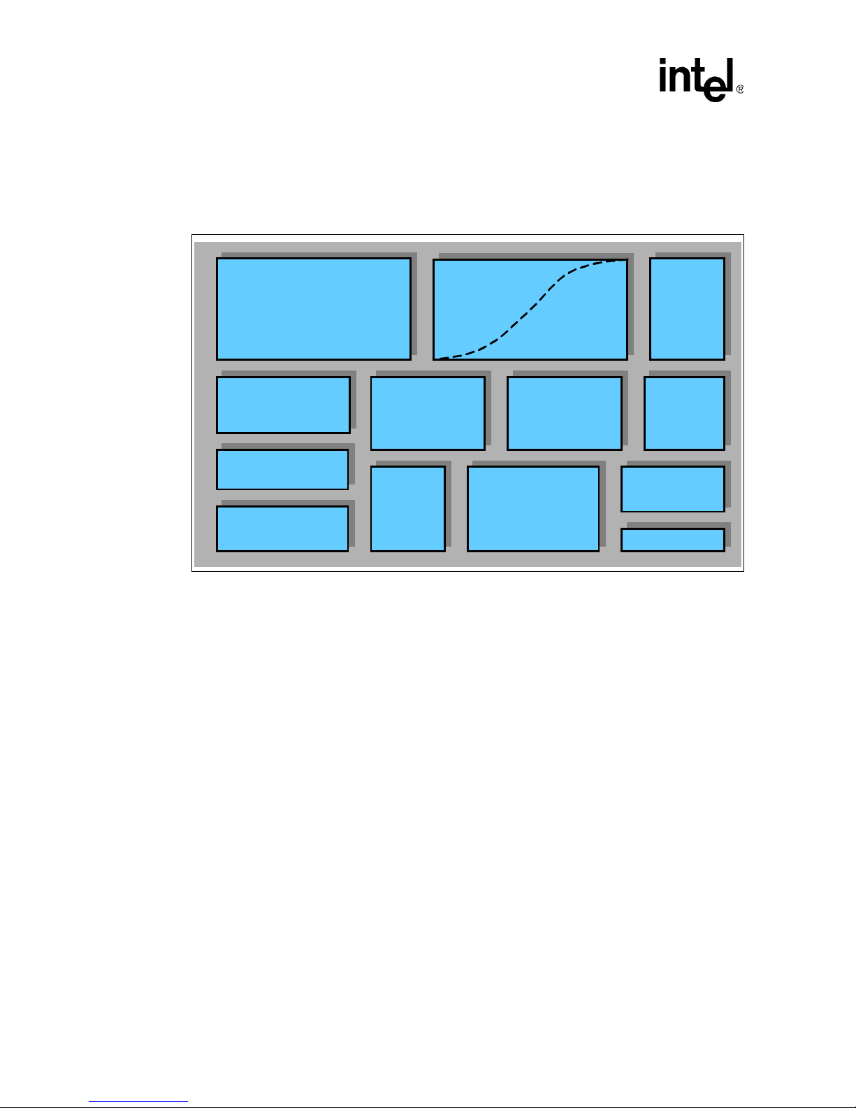
Figure 1-1 shows the major functional blocks of the Intel XSca le® core. The following sections
give a brief, high-level overview of these blocks.
1.2.2.1 Multiply /Accu mu late (MAC)
The MAC unit s upports early ter minat ion o f multi pli es/ac cumula tes in tw o cycle s and can sust ain a
throughput of a MAC operation every cycle. Several architectural enhancements were made to the
MAC to support audio coding algorithms, which include a 40-bit accumulator and support for
16-b i t packed data.
See Section 2.3, “Extensions to ARM Architecture” on page 2-23 for more details.
Figure 1-1. Architecture Features
Write Buffer
• 8 entries
• Full coalescing
Fill
Buffer
• 4 - 8 entries
Instruction Cache
• 32K or 16K bytes
• 32 ways
• Lockable by line
IMMU
• 32 entry TLB
• Fully associative
• Lockable by entry
DMMU
• 32 en try TLB
• Fully Associative
• Lockable by entry
JTAG
Debug
• Hardware Breakpoints
• Branch History Table
Branch Target
Buffer
• 128 entries
MAC
• Single Cycle
Throughput (16*32)
• 16-bit SIMD
• 40 bit Accumulator
Data Cache
• 32K or 16K bytes
• 32 ways
• wr-back or
wr-through
• Hit under
miss
Data RAM
• 28K or 12K
bytes
• Re-map of data
cache
Power
Mgnt
Ctrl
MiniData
Cache
• 2K or 1K
bytes
• 2 ways
Performance
Monitoring
Page 17

Developer’s Manual January, 2004 17
Intel XScale® Core Developer’s Manual
Introduction
1.2.2.2 Memory Manage men t
The Intel XScal e® core implements the Memory Management Unit (MMU) Architecture specified
in the ARM Arch itecture Referenc e Manual. The MMU provides access protection and virtual to
physical address tra n slation.
The MMU Architectur e also speci fies the caching policies for the in struct io n cache and d ata
memory. These policies are specified as page attributes and include:
• identifying code as cacheab le or non-cacheable
• selecting between the mini-da ta c ache or data cache
• write-back or write-through data caching
• enabling data write allocation policy
• and en ab l in g th e wr it e bu ffer to coales ce s tor es to ex ternal memory
Chapter 3, “Memory Management” discusses this in more detail.
1.2.2.3 Instruction Cache
The Intel XScale® core comes with either a 16 K or 32 K byte instruction cache. The size is
determined by the ASSP. The instruction cache is 32-way set associative and has a line size of
32 bytes. All requests that “miss” the instruction cache generate a 32-byte read request to ext ernal
memory. A mechanism to lock critical code within the cache is also provided.
Chapte r 4 , “I n s t r uc t io n Cac h e” discusses this in more detail.
1.2.2.4 Branch Target Buffer
The Intel XScale® core provides a Branch Target Buffer (BTB) to predict the outcome of branch
type instr u ctions. It provides storage f o r the target address of b r an ch type ins tructions and predicts
the next addre ss to present to the in struction cache when the current instruction address is tha t of a
branch.
The BTB holds 128 entries. See Chapter 5, “Branch Target Buffe r ” for more details.
1.2.2.5 Data Cache
The Intel XScale® core comes with either a 16 K or 32 K byte data cache. Th e size is determined
by the ASSP. Besides the main data cache, a mini-data cache is provid ed whos e size is 1/16
th
the
main data cache . So a 32K, 16 K byte main data cache would have a 2 K, 1 K byte mini-d ata ca che
respectively. The main data cach e is 32-way se t associative and th e mini-data cache is 2-way set
associative. Each cache has a line size of 32 bytes, supports write - through or write-back cachin g.
The data/mini-data cache is controlled by page attributes defined in the MMU Architecture and by
coprocessor 15.
Chapte r 6 , “D ata Cache” discusses all this in more detail.
The Intel XScale® core allows applications to re-configure a portion of the data cache as data
RAM. Software may place special tables or frequently used variables in this RAM. See
Section 6.4, “Re-config uring the Data Cache as Data RAM” on page 6-71 for more information on
this.
Page 18

18 January, 2004 Developer’s Manual
Intel XScale® Cor e Developer’s Manual
Introduction
1.2.2.6 Performance Monitoring
Perfor man ce mon it oring co u nter s hav e b een add ed to th e In te l XSca le® core th at ca n be con f igu red
to monitor variou s events in th e core. Th ese events allow a software deve lo per to measure cach e
efficiency, detect system bottlenecks and reduce the overall latency of programs.
Chapter8, “Performance Monitoring” discusses this in more det ail.
1.2.2.7 Power Managemen t
The Inte l X Scale® core incorporates a power and clock management unit that can assist ASSPs in
controlling their clocking and managing their power . T hes e features are described in Section 7.3,
“CP14 Register s” on page 7-96.
1.2.2.8 Debug
The Inte l X Scale® core supports software debugging through two instruction address break point
registers, one da ta-address breakpoint register , one data-address/mask br ea kpoint register , and a
trace b u ffer.
Chapter 9, “Software Debug” discusses thi s in m o r e de tail.
1.2.2.9 JTAG
Testabili ty is supported on the Intel XScale® core through the Test Access Port (TAP) Controller
implementation, which is based on IEEE 1149.1 (JTAG) Standard Test Acc es s Po rt and
Boundary-Scan Arc hitec ture. The purp ose of t he TAP contr oll er i s to suppo rt te st l ogic int er nal and
external to th e core such as built-in self-test and boundary-scan.
Appendix B discusses this in more detail.
Page 19

Developer’s Manual January, 2004 19
Intel XScale® Core Developer’s Manual
Introduction
1.3 Terminology and Convent ions
1.3.1 Number Representation
All numbers in this document can be assumed to be base 10 unless designated otherwise. In text and
pseudo code descriptions, hexadecimal numbers have a prefix of 0x and binary numbers have a prefix
of 0b. For example, 107 would be represented as 0x6B in hexadecimal and 0b1101011 in binary.
1.3.2 Ter minology and Acronyms
ASSP Application Specific Standard Product
Assert This term refers to the logically active value of a signal or bit.
BTB Branch Target Buffer
Clean A clean operation upda tes ext ern al memory with the con tents of t he spe cif ied li ne in
the data /min i- da ta ca ch e i f an y o f t he dirt y b its a re s et a nd t he l in e is v al id. Th ere ar e
two dirty bits ass o ciated with each line in the cache so only the portion that is dirty
will get written back to external memory.
After this operation, the line is still valid and both dirty bi ts are deasserted.
Coalescing Coalescing means bringing together a new store operation with an existing store
operation already resident in the write buffer. The new store is placed in the same
write buffer entr y as an existing store when the address of the new store falls in the
4 word aligned add ress of the exis ting entry. This includes, in PCI termin ology , writ e
merging, write collapsing, and write combining.
Deassert This term refers to the logica lly inactive value of a signal or bit.
Flush A flush oper ati on inva li dates the l ocati on(s) i n t he c ache by d easse rting t he vali d bi t.
Individual e ntries ( lin es) may be flush ed or t he ent ire c ache may be fl ushed wit h one
command. Once an entry is flushed in the cache it can no longer be used by the
program.
XSC1 XSC1 r efers to a variant of the Intel XScale® core denoted by a CoreGen
(Coprocessor 15 , ID Regis ter) value of 0x1. This varia nt has a 2 counter pe rformance
monitor and a 5-bit JTAG instruction register. See Table 7-4, “ID Register” on
page 7-81 for more details.
XSC2 XSC2 r efers to a variant of the Intel XScale® core denoted by a CoreGen
(Coprocessor 15 , ID Regis ter) value of 0x2. This varia nt has a 4 counter pe rformance
monitor and a 7-bit JTAG instruction register. See Table 7-4, “ID Register” on
page 7-81 for more details.
Reserved A reserved field is a field th at may be us ed by an im pl ement at ion . I f th e in iti al val ue
of a reserved field is supplied by software, this value must be zero. Software should
not modify reserved fields or depend on any values in reserved fields.
Page 20

20 January, 2004 Developer’s Manual
Intel XScale® Cor e Developer’s Manual
Introduction
This Page Intentionally Left Blank
Page 21

Developer’s Manual January, 2004 21
Intel XScale® Core Developer’s Man u al
Programming Model
Programming Model 2
This chapter desc ribes the programming model of the Intel XScale® core, namely the
implementation options and extensions to the ARM Version 5TE architecture.
2.1 ARM Architecture Compatibility
The Intel XScale® core implements the in teger instruction set arc hitecture specified in ARM
V5TE. T refers to the Thumb instr uction set and E refers to the DSP-Enhanced ins truction set.
ARM V5TE in tro duce s a f e w more arc hi tec tu re fe at ures ov er ARM V4, sp ecif ica ll y the add iti on of
tiny pages (1 Kbyte), a new instruction (CLZ) that counts the leading zeroes in a data value,
enhanced ARM-Thumb transfer instructions and a modification of the sys tem control coprocessor ,
CP15.
2.2 ARM Architecture Implementation Options
2.2.1 Big Endian versus Little Endian
The Intel XScale® core supports both big and little endian data representation. The B-bit of the
Control Register (Coproces sor 15, register 1, bit 7) selects big and lit tl e endia n mode. To run in big
endian mode, the B bit must be se t before attempting any sub-word acce sses to memory, or
undefined results will occur. Note that this bit takes effect even if the MMU is disabled.
2.2.2 26-Bit Architecture
The Intel XScale® core does not support 26-bit architecture.
2.2.3 Thumb
The Intel XScale® core supports the Thumb instruction set.
Page 22

22 January, 2004 Developer’s Manual
Intel XScale® Cor e Developer’s Manual
Programm i ng M odel
2.2.4 ARM DSP-Enh an ce d In stru ct ion Set
The Inte l X Scale® core implements the ARM DSP-enhanced instruction set which is a set of
instructi ons that boost the performanc e of s ignal processing appl ications. There are new multiply
instructions that operate on 16-bit data values and new saturation instructions. Some of the new
instructions are:
• SMLAxy 32<=16x16+32
• SMLAWy 32<=32x16+32
• SMLALxy 64<=16x16+64
• SMULxy 32<=16x16
• SMULWy 32<=32x16
• QADD adds two registers and saturates the result if an overflow occurred
• QDADD doubles and satura tes one of the input registers then add and saturate
• QSUB subtracts two registers and saturates the result if an overflow occurred
• QDSUB doubles and saturates one of the input re gis ters then subtract and saturate
The Intel XScale® core also implements LD RD, S TRD and PLD instructions with the following
implementation notes:
• PLD is interpreted as a read operat ion by the MMU and is ignored by the data bre akpoint unit
(i.e., PLD will neve r generate data breakpoi nt events).
• PLD to a non-cacheable page performs no action. Also, if the targeted cache line is already
resident, this instruction has no af fect.
• Both LDRD and STRD instructions will generate an alignment exception when the address
bits [2:0] = 0b100.
MCRR and MRRC are only supported on the Intel XScale® core when di r ected to coprocessor 0
and are used to access the internal accumulator. See Section 2.3.1.2 for more information. Access
to coprocesso rs 15 and 14 generate an undefined ins truction exception. Refer to the Intel XScale
®
core implementa tion option section of the ASSP architecture specifi ca tion for the behavior when
accessi ng al l ot h er co p r oc es s o r s.
2.2.5 Base Register Update
If a data abort is signalled on a memory instruction that specifies writeback, the contents of the
base register will not be updated. This holds for all load and store instructions. This behavior
matches that of the first generation StrongARM processor and is referred to in the ARM V5TE
archite ct u r e as th e Base Restored Abort Model.
Page 23

Developer’s Manual January, 2004 23
Intel XScale® Core Developer’s Man u al
Programming Model
2.3 Extensions to ARM Architecture
The Intel XScale® core made a few extensions to the ARM Version 5TE architecture to meet the
needs of various marke ts and design requirements. The following is a list of the extensions which
are discussed in the next sections.
• A DSP coprocessor (CP0) has been added that contains a 40-bit accumulator and eight new
instructions.
• New page attributes were added to the page table descriptors. The C and B page attribute
encoding was extended by one more bit to allow for more encodings: write allocate and
mini-data cache. An ASSP definable attribute (P bit) was also added.
• Additional functionality has been added to coprocessor 15. Coprocessor 14 was also created.
• Enhancements were made to the Eve n t Ar chitecture , which include instruction cache and data
cache parity error ex ceptions, breakpoint events, and imprecise external data aborts.
2.3.1 DSP Coprocessor 0 (CP0)
The Intel XScale® core adds a DSP coprocessor to the architecture for the purpose of increasing
the performance and the pre cision of audio processing algorithms. This coproc essor contains a
40-bit accumulator and 8 new instructions.
Note: Products using the Intel XScale® core may extend the definition of CP0. If this is the case, a
complete definition can be found in the Intel XScale
®
core implementation option section of the
ASSP architecture specification. For this very reason, software should not rely on behavior that is
specific to the 40-bit length of the accumulator, since the length may be extended.
The 40-bit accumulat or is refe renced by several new instructi ons that were added to the
architecture; MIA, MIAPH and MIAxy are multiply/accumulate instruc tions that ref erence the
40-bit accumulator instead of a register specified accumulator. MAR a nd MRA pr ovide the a b ility
to read and write the 40-bit accumulator.
Access to CP0 is always allowed in all processor modes when bit 0 of the Coprocessor Access
Register is set. Any access to CP0 when this bit is clear will cause an undefined exception. (See
Section 7.2.15, “Register 15: Coprocessor Access Register” on page 7-94 for more details).
Note: Only pr ivilege d softwar e can set thi s bi t in th e Coproce s so r Ac cess Reg is ter.
The 40-bit a ccumulator will need to be sa ved on a context switch if mu ltiple proces ses are using it.
Two new instruction formats were added for coproc ess or 0: Multiply with Internal Accumulate
Format and Internal Accumulate Access Format . The formats and instructions are described next .
Page 24
24 January, 2004 Developer’s Manual
Intel XScale® Cor e Developer’s Manual
Programm i ng M odel
2.3.1.1 Multiply With Internal Accumulate Format
A new multiply format has been created to define operations on 40-bit accumulators. Table 2-1,
“Mul tiply wi t h I nterna l A ccumulate For mat” on page 2-2 4 shows the layout of the new format.
The opcode for this forma t lies within the coprocessor register transfer instruction type. These
instructions have their own syntax.
Two new fields were created for this format, acc and opcode_3. The acc field specifies 1 of 8
intern al accumu lators to op erate on an d opcode_3 defines the operation for this format. The Intel
XScale
®
core defines a single 40-bit accum ulator referred to as acc0; future implementations may
define multiple internal accumulators. The Intel XScale
®
core uses opcode_3 to de fine six
instructions, MIA, MIAPH, MIAB B, MIABT, MIATB and MIATT.
Table 2-1. Multiply with Internal Accumulate Format
31 30 29 28 27 26 25 24 23 22 21 20 19 18 17 16 15 14 13 12 11 10 9 8 7 6 5 4 3 2 1 0
cond 1 1 1 0 0 0 1 0 opcode_3 Rs 0 0 0 0 acc 1 Rm
Bits Description Notes
31:28 cond - ARM condition codes -
19:16
opcode_3 - specifies the type of multiply with
internal ac c umulate
The Intel XScale® core defines the following:
0b0000 =
MIA
0b1000 = MIAPH
0b1100 = MIABB
0b1101 = MIABT
0b1110 = MIATB
0b1111 = MIATT
The effect of all other encodings are
unpredictable.
15:12 Rs - M u ltiplier
7:5 acc - select 1 of 8 ac cumulators
The Intel XScale® core only implements acc0;
access to any other acc has an unpredictable
effect.
3:0 Rm - Multiplicand -
Page 25
Developer’s Manual January, 2004 25
Intel XScale® Core Developer’s Man u al
Programming Model
The MIA instruction operates similarly to MLA except t h at the 40-bit accumulator is used. MIA
multiplie s the signed value in register Rs (multiplier) by the signed value in register Rm
(multiplicand) and then adds the result to the 40-bit accumulator ( acc0).
MIA does not support unsigned multiplication; all values in Rs and Rm will be interpreted as
signed data val ues. MIA is useful f or operat ing on sig ned 16-bit dat a that was lo aded int o a general
purpose register by LDRSH.
The instruction is only executed if the condition specified in the instruction matches the condition
code status.
The MIAPH instruction performs two16-bit si gned multiplies on packed half word data and
accumulates these to a single 40-bit accumulator. The first signed multiplication is performed on
the lower 16 bits of the value in register Rs with the lower 16 bits of the value in register Rm. The
second signed multiplication is perfo rme d on the upper 16 bits of the value in register Rs with the
upper 16 bits of the value in register Rm. Both si gned 32-bit products are si gn extended and then
added to the value in the 40-bit accumulator (acc0).
The instruction is only executed if the condition specified in the instruction matches the condition
code status.
Table 2-2. MIA{<cond>} acc0, Rm, Rs
31 30 29 28 27 26 25 24 23 22 21 20 19 18 17 16 15 14 13 12 11 10 9 8 7 6 5 4 3 2 1 0
cond 1 1 1 0 0 0 1 0 0 0 0 0 Rs 0 0 0 0 0 0 0 1 Rm
Operation: if ConditionPassed(<cond>) then
acc0 = (Rm[31:0] * Rs[31:0])[39:0] + acc0[39:0]
Exceptions:none
Qualifiers Condition Code
No condition code flags are updated
Notes: Early termination is supported. Instruction timings can be found
in Section 10.4.4, “Multiply Instruction Timings” on page 10-168.
Specifying R15 for register Rs or Rm has unpredictable results.
acc0 is defined to be 0b000 on the core.
Table 2-3. MIAPH{<cond>} acc0, Rm, Rs
31 30 29 28 27 26 25 24 23 22 21 20 19 18 17 16 15 14 13 12 11 10 9 8 7 6 5 4 3 2 1 0
cond 1 1 1 0 0 0 1 0 1 0 0 0 Rs 0 0 0 0 0 0 0 1 Rm
Operation: if ConditionPassed(<cond>) then
acc0 = sign_extend(Rm[31:16] * Rs[31:16]) +
sign_extend(Rm[15:0] * Rs[15:0]) +
acc0[39:0]
Exceptions:none
Qualifiers Condition Code
S bit is always cleared; no condition code flags are updated
Notes: Instruction timings can be found
in Section 10.4.4, “Multiply Instruction Timings” on page 10-168.
Specifying R15 for register Rs or Rm has unpredictable results.
acc0 is defined to be 0b000 on the core
Page 26

26 January, 2004 Developer’s Manual
Intel XScale® Cor e Developer’s Manual
Programm i ng M odel
The MIAxy instruction performs one16-bit signed multiply and accumulates these to a single
40-bit accumulator. x refers to either the upper half or lower half of regist er Rm (multiplica nd) and
y refers to the upper or lower half of Rs (multiplier). A value of 0x1 will sele ct bits [31:16] of the
register which is specified in the mnemonic as T (for top ) . A val ue of 0x0 will select bits [15:0] of
the register which is speci f ied in the mnemonic as B (for bottom).
MIAxy does not support unsigned multiplication; all values in Rs and Rm will be interpreted as
signed data values.
The instruction is only executed if the condition specified in the instruction matches the condition
code status.
Table 2-4. MIAxy{<cond>} acc0, Rm, Rs
31 30 29 28 27 26 25 24 23 22 21 20 19 18 17 16 15 14 13 12 11 10 9 8 7 6 5 4 3 2 1 0
cond 1 1 1 0 0 0 1 0 1 1 x y Rs 0 0 0 0 0 0 0 1 Rm
Operation: if ConditionPassed(<cond>) then
if (bit[17] == 0)
<operand1> = Rm[15:0]
else
<operand1> = Rm[31:16]
if (bit[16] == 0)
<operand2> = Rs[15:0]
else
<operand2> = Rs[31:16]
acc0[39:0] = sign_extend(<operand1> * <operand2>) + acc0[39:0]
Exceptions:none
Qualifiers Condition Code
S bit is always cleared; no condition code flags are updated
Notes: Instruction timings can be found
in Section 10.4.4, “Multiply Instruction Timings” on page 10-168.
Specifying R15 for register Rs or Rm has unpredictable results.
acc0 is defined to be 0b000 on the core.
Page 27
Developer’s Manual January, 2004 27
Intel XScale® Core Developer’s Man u al
Programming Model
2.3.1.2 Internal Accumulator Access Format
The Intel XScale® core defines a new instruction format for acces sing internal accumulators in
CP0. Table 2-5, “Internal Accumulator Access Format” on pa ge 2-27 shows that the opcode falls
into the coprocessor register transfer space.
The RdHi and RdLo fields allow up t o 64 bits of data transfer betwee n StrongARM re gist ers an d an
internal accumulator. The acc field specifies 1 of 8 internal accumulators to transfer data to/from.
The core implements a sin gle 40-bit accum u lator referred to as acc0; future implementations can
specify multiple internal accumulators of varying sizes, up to 64 bits.
Access to the internal accumulator is allowed in all processor modes (user and privileged) as long
bit 0 of the Coproces sor Access Register is set. (See Section 7.2.15, “Register 15: Coprocessor
Access Register” on page 7-94 for more details).
The Intel XScale® core imp le m e nts two ins t r uc tions MAR and MRA that move two ARM
registers to acc0 and move acc0 to two ARM regis ters, respectively.
Note: MAR has t h e same encoding as MCRR (to coproc essor 0) and MRA has the s a m e en c od i n g as
MRRC (to coprocessor 0). These instructions move 64-bits of data to/from ARM registers from/t o
coprocessor registers. MCRR and MRRC are defined in ARM’s DSP ins truction set.
Disassemblers not aware of MAR and MRA will produce the following syntax:
MCRR{<cond>} p0, 0x0, RdLo, RdHi, c0
MRRC{<cond>} p0, 0x0, RdLo, RdHi, c0
Table 2-5. Internal Accumulator Access For mat
31 30 29 28 27 26 25 24 23 22 21 20 19 18 17 16 15 14 13 12 11 10 9 8 7 6 5 4 3 2 1 0
cond 1 1 0 0 0 1 0 L RdHi RdLo 0 0 0 0 0 0 0 0 0 acc
Bits Description Notes
31:28 cond - ARM condition codes -
20
L - move to/from internal accumulator
0= move to internal accumulator (MAR)
1= move from internal accumulator (MRA)
-
19:16
RdHi - specifies the high order eight (39:32)
bits of the internal accumulator.
On a read of the acc, this 8-bit high order field
will be sign extended.
On a write to the acc, the lower 8 bits of this
register will be written to acc[39:32]
15:12
RdLo - specifies t he low order 32 bits of t he
internal accumulator
-
7:4 Should be zero
This field could be used in future
implementatio ns to specify the type of
saturati on to pe rf orm o n t he r ead o f an in ter na l
accumulator. (e.g., a signed saturation to
16-bits m ay be usef ul for some filter
algorithms.)
3 Should be zero
-
2:0 acc - specifies 1 of 8 internal accumulators
The core only imple ments acc0; access to
any other acc is unpredictable
Page 28
28 January, 2004 Developer’s Manual
Intel XScale® Cor e Developer’s Manual
Programm i ng M odel
The MAR instruction moves the value in register RdLo to bits[31:0] of the 40-bit accumulator
(acc0) and moves bits [7:0] of the value in registe r RdHi into bits[39:32] of acc 0.
The instruction is only executed if the condition specified in the instruction matches the condition
code status.
This instruction executes in any pr ocessor mode.
The MRA instruction moves the 40-bit accumulator value (acc0) into two regi sters. Bits[31:0] of
the value in acc0 are moved into the register RdLo. Bits[39:32] of the value in acc0 are sign
extended to 32 bits and moved into the regi st er RdHi.
The instruction is only executed if the condition specified in the instruction matches the condition
code status.
This instruction executes in any pr ocessor mode.
Table 2-6. MAR{<cond>} acc0, RdLo, RdHi
31 30 29 28 27 26 25 24 23 22 21 20 19 18 17 16 15 14 13 12 11 10 9 8 7 6 5 4 3 2 1 0
cond 1 1 0 0 0 1 0 0 RdHi RdLo 0 0 0 0 0 0 0 0 0 0 0 0
Operation: if ConditionPassed(<cond>) then
acc0[39:32] = RdHi[7:0]
acc0[31:0] = RdLo[31:0]
Exceptions:none
Qualifiers Condition Code
No condition code flags are updated
Notes: Instruction timings can be found in
Section 10.4.4, “Multiply Instruction Timings” on page 10-168
Specifying R15 as either RdHi or RdLo has unpredictable results.
Table 2-7. MRA{<cond>} RdLo, RdHi, acc0
31 30 29 28 27 26 25 24 23 22 21 20 19 18 17 16 15 14 13 12 11 10 9 8 7 6 5 4 3 2 1 0
cond 1 1 0 0 0 1 0 1 RdHi RdLo 0 0 0 0 0 0 0 0 0 0 0 0
Operation: if ConditionPassed(<cond>) then
RdHi[31:0] = sign_extend(acc0[39:32])
RdLo[31:0] = acc0[31:0]
Exceptions:none
Qualifiers Condition Code
No condition code flags are updated
Notes: Instruction timings can be found in
Section 10.4.4, “Multiply Instruction Timings” on page 10-168
Specifying the same register for RdHi and RdLo has unpredictable
results.
Specifying R15 as either RdHi or RdLo has unpredictable results.
Page 29

Developer’s Manual January, 2004 29
Intel XScale® Core Developer’s Man u al
Programming Model
2.3.2 New Page Attributes
The Intel XScale® core extends the page attributes defined by the C and B bits in the page
descriptor s wit h an add itional X bit. This bit al lows four more attributes to be encoded when X=1.
These new encodings include allocating data for the mini-data cache and write-allocate caching. A
full descripti on of th e encodi ngs can be found in Section 3.2.2, “Memory Attri bute s” on page 3-38.
The Intel XScale® core retains ARM definitions of the C and B encoding when X = 0, which is
differe nt than the StrongARM prod ucts. The memory attribu te for the mini-data cach e has bee n
moved and replaced with the write-through caching attribute.
When write-alloc ate is enabled, a store operatio n th at misses the data cache (cacheable data only)
will generate a line fill. If disabled, a lin e fill only occurs when a load operation misses the data
cache (cacheable data only).
Write-through caching causes all store operat ions to be written to memory, whether the y are
cacheable or not cacheable. This feature is use ful for maintaining data ca che coherency.
The Intel XSca le® core also adds a P bit in the first level descriptors to allow an ASSP to identify a
new memory attribute. Refer to the Intel XScal e
®
core implementation option section of the ASSP
architecture s pecification to find out how the P bit has been defined. Bit 1 in the Control Register
(coprocessor 15, register 1, opcode=1) is used to assigned the P bit memory attribute for memory
accesses made during page table walks.
These attributes are programmed in the translation table descriptors, which are highlighted in
Table 2-8, “First-level Descriptors” on page 2-30, Table 2-9, “Second-level Descriptors for Coarse
Page Table” on page 2-30 and Tab le 2-10, “Second-leve l Descriptors for Fine Page Table” on
page 2-30. Two second-level descriptor formats have been defined for the core, one is us ed for the
coarse page table and the other is used for the fine page table.
Page 30
30 January, 2004 Developer’s Manual
Intel XScale® Cor e Developer’s Manual
Programm i ng M odel
The TEX (T ype Extension) fiel d is pres ent in several of the descriptor types. In the core, only the
LSB of this field is defined; this is called the X bit. The remaining bits s hould be programmed as
zero (SBZ).
A Small Page descriptor does not have a TEX field. For these descriptors, TEX is implicitly zero;
that is, they operate as if the X bit had a ‘0’ valu e.
The X bit, when set, modi fies the meaning of the C and B bits. Des cription of page attributes and
their encoding can be found in Chapter 3, “Memory Management”.
Table 2-8. First-level Descriptors
31 30 29 28 27 26 25 24 23 22 21 20 19 18 17 16 15 14 13 12 11 10 9 8 7 6 5 4 3 2 1 0
SBZ 0 0
Coarse page table base address P Domain SBZ 0 1
Section base addre ss SBZ TEX AP P Domain 0 C B 1 0
Fine page table base address SBZ P Domain SBZ 1 1
Table 2-9. Second-level Descriptors for Coarse Page Table
31 30 29 28 27 26 25 24 23 22 21 20 19 18 17 16 15 14 13 12 11 10 9 8 7 6 5 4 3 2 1 0
SBZ 0 0
Large page base address TEX AP3 AP2 AP1 AP0 C B 0 1
Small page base address AP3 AP2 AP1 AP0 C B 1 0
Extended small page base address SBZ TEX AP C B 1 1
Table 2-10. Second-level Descriptors for Fine Page Table
31 30 29 28 27 26 25 24 23 22 21 20 19 18 17 16 15 14 13 12 11 10 9 8 7 6 5 4 3 2 1 0
SBZ 0 0
Large page base ad dres s TEX AP3 AP2 AP1 AP0 C B 0 1
Small page base address AP3 AP2 AP1 AP0 C B 1 0
Tiny Page Base Address TEX AP C B 1 1
Page 31

Developer’s Manual January, 2004 31
Intel XScale® Core Developer’s Man u al
Programming Model
2.3.3 Additions to CP15 Functionality
T o ac com mod ate t he f u nct io nal ity in t he In te l XS cale® core, regist ers i n CP15 a nd CP14 h ave been
added or augmented. See Chapter 7, “Configuration” for details.
At times it is necessary to be able to guaran tee exactly when a CP15 update takes effect. For
example, when enabling memory address translation (turning on the MMU), it is vital to know
when the MMU is actual ly guaran teed to be in operat ion. To address this need, a processor -spec if ic
code sequence is defined for the core. T he sequence -- called CP WAIT -- is shown in Example 2-1
on page 2-31.
Example 2-1. CPWAIT: Cano nical me thod to wait for CP15 update
When setting multi ple CP15 registers, sy st em software may opt to delay the assurance of their
update. This is acco mplished by executing CPWAIT only after the sequence of M CR instruct io ns.
Note: The CPWAIT sequence guarant ees that CP15 side-effects are complet e by the time the CPWAIT is
complete. It is pos sible, however, that the CP15 side-effect will take place before CPWAIT
completes or is iss ued. Programmers should take care tha t this does not affect the correctness of
their code.
;; The following macro should be used when software needs to be
;; assured that a CP15 update has taken effect.
;; It may only be used while in a privileged mode, because it
;; accesses CP15.
MACRO CPWAIT
MRC P15, 0, R0, C2, C0, 0 ; arbitrary read of CP15
MOV R0, R0 ; wait for it
SUB PC, PC, #4 ; branch to next instruction
; At this point, any previous CP15 writes are
; guaranteed to have taken effect.
ENDM
Page 32

32 January, 2004 Developer’s Manual
Intel XScale® Cor e Developer’s Manual
Programm i ng M odel
2.3.4 Event Architecture
2.3.4.1 Exception Summary
Table 2-11 shows all the exceptions that the core may generate, and the attributes of each.
Subsequent sections give details on each exception.
2.3.4.2 Event Priority
The Intel XScale® core follows the exception p r iority specified in the ARM Architecture Reference
Manual. The process or has additional exceptions that might be generated while debugging. For
information on these debug exceptions, see Chapter 9, “Software Debug”.
Table 2-11. Exception Summary
Exception Description Exception Type
a
a. Exception types are those described in the ARM, section 2.5.
Precise? Updates FAR?
Reset Reset N N
FIQ FIQ N N
IRQ IRQ N N
External Instruc tio n Prefetch Y N
Instruction MMU Prefetch Y N
Instruction Cache Parity Prefetch Y N
Lock Abor t Data Y N
MMU Data Data Y Y
External Data Data N N
Data Cache Parity Data N N
Software Interrupt Software Interrupt Y N
Undefined Instr uction Undefined Instruction Y N
Debug Events
b
b. Refer to Chapter 9, “Software Debug” for more details
varies varies N
Table 2-12. Event Priority
Exception Priority
Reset 1 (Highest)
Data Abort (Precise & Imprecise) 2
FIQ 3
IRQ 4
Prefetch Abort 5
Undefined Instru ction, SWI 6 (Lowest)
Page 33

Developer’s Manual January, 2004 33
Intel XScale® Core Developer’s Man u al
Programming Model
2.3.4.3 Prefetch Aborts
The Intel XScale® core detects three types of prefetch aborts: Inst ruction MMU abort, external
abort on an instructi on access, and an instructi on ca che parity error. These aborts are des cribed in
Table 2-13.
When a pref etc h abo r t oc curs , h ardwa re rep ort s t he hi ghe st prior ity on e in th e ex ten ded S t atu s fi eld
of the Fault St atus Register. The value plac ed in R14_ABORT (the link register in abort mode) is
the address of the aborted instruction + 4.
T able 2-13. Encoding of Fault Status for Prefetch Aborts
Priority Sources FS[10,3:0]
a
a. All other encodings not listed in the table are reserved.
Domain FAR
Highest
Instruction MMU Exception
Several exceptions can generate this encoding:
- translation faults
- domain faults, and
- permis sion faults
It is up to software to figure out w hich one occurred.
0b10000 invalid invalid
External Instruction Error Exception
This exception occurs when th e external m em ory system
reports an error on an instruction cache fetch.
0b10110 invalid invalid
Lowest Instruction Cache Parity Error Exception 0b11000 invalid invalid
Page 34

34 January, 2004 Developer’s Manual
Intel XScale® Cor e Developer’s Manual
Programm i ng M odel
2.3.4.4 Data Abor ts
Two types of data aborts exist in the Intel XScale® core: precise and imprecise. A precise data
abort is defined as one where R14_ABORT always contains the PC (+8) of the instruction that
caused the exception. An imprecise abort is one where R14_ABORT contains the PC (+4) of the
next instruction to execute and not the add r ess of the instruction that caused the abort. In other
words, instruction execution wil l have advanced beyond the instruction that cause d the data abort.
On the core, precise data aborts are recoverable a nd imprecise data aborts are not recoverable.
Precise Data Aborts
• A lock abort is a precise data abo r t; the extended Status field of the Faul t Status Register is set
to 0xb10100. This abort occurs when a lock operation directed to the MMU (instruction or
data) or instr uction cache causes an exception, due to either a translation fault, acces s
permission fault or external bus fault.
The Fault Address Register is undefined and R14_ABORT is the address of the aborted
instruction + 8.
• A data MMU abort is precise. These are due to an alignment fault, translation fault, domain
fault, permis sion fa ult or exte rnal dat a abort on an MMU translati on. The sta tus fie ld is set to a
predetermined ARM definition which is shown in Table 2-14, “Encoding of Fault Status for
Data Aborts” on page 2-34.
The Fault Address Register is set to the effective data address of the instruction and
R14_ABORT is the address of the ab orted instruction + 8.
Imprecise data aborts
• A data cache parity error is imprecise; the extended Status field of the Fault Status Registe r is
set to 0xb11000.
• All external data aborts except for those generated on a data MMU translation are imprecise.
The Fault Address Register for all imprecise data aborts is unde fined and R14_ABORT is the
address of the next instruction to execute + 4, which is the same for both ARM and Thumb mode.
Table 2-14. Encoding of Fault Status for Data Aborts
Priority Sources FS[10,3:0]
a
a. All other encodings not listed in the table are reserved.
Domain FAR
Highest Alignment 0b000x1 invalid valid
External Abort on Translation
First level
Second le vel
0b01100
0b01110
invalid
valid
valid
valid
Translation
Section
Page
0b00101
0b00111
invalid
valid
valid
valid
Domain
Section
Page
0b01001
0b01011
valid
valid
valid
valid
Permission
Section
Page
0b01101
0b01111
valid
valid
valid
valid
Lock Abort
This data abort occurs on an M M U lock oper ation (dat a or
instruc ti on TLB) or on an Instruction Cach e lock operation.
0b10100 invalid invalid
Imprecise External Data Abort 0b10110 invalid invalid
Lowest Data Cache Parity Error Exception 0b11000 invalid invalid
Page 35

Developer’s Manual January, 2004 35
Intel XScale® Core Developer’s Man u al
Programming Model
Although the core guaran tees the Base Restored Abort Model for precise aborts, it cannot do so in
the case of imprecise aborts. A Data Abort handler may encou nter an updated base register if it is
invoked because of an imprecise abort.
Imprecise data aborts may create scenarios difficult for an abort handler to recover. Both external data
aborts and data cache parity errors may result in corrupted targeted register data. Because these faults
are imprecise, it is possible corrupted data will have been used before the Data Abort fault handler is
invoked. Because of this, software should treat imprecise data aborts as unrecoverable.Even memory
accesses marked as “stall until complete” (see Section 3.2.2.4) can result in imprecise data abor ts.
For thes e ty pe s of ac cesses, th e fa u l t is s o mewhat less im p r ecise than th e ge neral cas e: it is
guaranteed to be raised with in thr ee instruc tions of the inst r uction that caused it. In other wor ds, if
a “stall until complete” LD or ST instruction triggers an imprecise fault, then that fault will be seen
by the program within three instructions.
With this kn o w l e d g e, it is p o ss i bl e to w r ite code that accesses “stall until comp le te” memo r y with
impunity. Simply place several NOP instructions after such an access. If an imprecise fault occurs,
it will do so during the NOPs; the data abort h andler will se e identical register and me mo ry state as
it would with a precise exce ption, and so should be able to re cover. An example of thi s is shown in
Example 2-2 on page 2-35.
If a system design precl udes events that could cause external aborts, th en s uch precautions are not
necessary.
Mult iple Dat a A b orts
Multiple data aborts may be detected by hardware but only the highest priority one will be
reported. If the reported data abort is precise, soft ware can corre ct the cause of the abort and
re-exec ute the aborted ins truction. I f th e lower priorit y abort still exists, it will be reported.
Software can handle each abort separately unti l the instruction successfully executes.
If the reported data abort is imprecise, software needs to check the SPSR to see if the previous
context was exec uting in abort mode. If this is the case, the link back to the c urrent process has
been lost and the dat a abort is unrecoverable.
2.3.4.5 Events from Preload Instructions
A PLD inst ruction will never cause the Data MMU to faul t for any of the following reasons:
• Domain Fault
• Permission Fault
• Translation Fault
If execution of the PLD would cause one of the above faults, then the PLD causes no effect.
Example 2-2. Shielding Code from Potential Imprecise Aborts
;; Example of code that maintains architectural state through the
;; window where an imprecise fault might occur.
LD R0, [R1] ; R1 points to stall-until-complete
; region of memory
NOP
NOP
NOP
; Code beyond this point is guaranteed not to see any aborts
; from the LD.
Page 36

36 January, 2004 Developer’s Manual
Intel XScale® Cor e Developer’s Manual
Programm i ng M odel
This feature allows softwa re t o iss ue PLDs sp eculatively. For exampl e, Example 2-3 on page 2-36
places a PLD instruction early in the lo op. This PLD is used to fetc h data for the next loop
iteration. In this example, the list is terminated with a node that has a null pointer. When execution
reaches the end of the list, the PLD on address 0x0 will not cause a f ault. Rather, it will be ignored
and the loop will te rminate normally.
2.3.4.6 Debug Events
Debug events are covered in S ection 9.5, “Debug Exceptions” on page 9-126.
Example 2-3. Speculatively issuing P LD
;; R0 points to a node in a linked list. A node has the following layout:
;; Offset Contents
;;---------------------------------;; 0 data
;; 4 pointer to next node
;; This code computes the sum of all nodes in a list. The sum is placed into R9.
;;
MOV R9, #0 ; Clear accumulator
sumList:
LDR R1, [R0, #4] ; R1 gets pointer to next node
LDR R3, [R0] ; R3 gets data from current node
PLD [R1] ; Speculatively start load of next node
ADD R9, R9, R3 ; Add into accumulator
MOVS R0, R1 ; Advance to next node. At end of list?
BNE sumList ; If not then loop
Page 37

Developer’s Manual January, 2004 37
Intel XScale® Core Developer’s Manual
Memory Ma nagemen t
Memory Management 3
This chapter describes the memory managemen t unit implemented in the Intel XScale® core.
3.1 Overview
The Intel XScal e® core implements the Memory Management Unit (MMU) Architecture specified
in the ARM Arch itecture Referenc e Manual. To accelera te virtual to physical addres s translation,
the core uses both an instruction Translation Look-aside Buffer (TLB) and a data TLB to cache the
latest translations. Each TLB holds 32 entries and is fully-associative. Not only do the TLBs
contain the translated addresses, but also the access rights for memory references.
If an instruction or data TLB miss occurs, a hardware translation-table-walking mechanism is
invoked to translate the virtual address to a physical address. Once translated, the physical address is
placed in the TLB along with the access rights and attributes of the page or section. These translations
can also be locked down in either TLB to guarantee the performance of critical routines.
The Intel XScale® core allows system software to associate various attributes with regions of
memory:
• cacheable
• bufferable
• line allocate policy
• write policy
• I/O
• mini Data Cac he
• Coalescing
• an ASSP definable attribute - P bit (Refer to the Intel XScale
®
core impleme n tation section of
the ASSP architecture specificati on for mor e info rmation.)
See Section 3.2.2, “Memory Attributes” on page 3-38 for a descript ion of page attributes and
Section 2.3.2, “New Page Attribut es” on page 2-29 to find out where these attributes have been
mapped in the MMU descriptors.
Note: The virtual address with whi ch the TLBs are accessed may be remapped by the PID register. See
Section 7.2.13, “Register 13: Process ID” on page 7-91 for a description of the PID register.
Page 38

38 January, 2004 Developer’s Manual
Intel XScale® Cor e Developer’s Manual
Memory Management
3.2 Architecture Model
3.2.1 Version 4 vs. Version 5
ARM* MMU Version 5 Architecture intro duces the support of tiny pages , which are 1 KByte in
size. The reserved field in the first-level de sc riptor (encoding 0b11) is used as the fine page table
base address. The exact bit fields and the format of the first and second-level desc riptors can be
found in Section2.3.2, “New Page Attributes” on page 2-29.
3.2.2 Memory Attributes
The attributes as sociated with a particular region of memory are configured in the memory
management page table and control the behavior of accesses to the ins truction cache, data cache,
mini-data cache and the write buffer. These attributes are ignored when the MMU is disa bled.
To allow compatibility with older system software, the new core attribut es take advantage of
encodi ng sp ac e in th e d es c r ip t ors th a t w as f o rm er l y res er v ed .
3.2.2.1 Page (P) Attribute Bit
The P bi t allows an ASSP to assign its own page attribute to a memory region. This bit is only
presen t in th e fi r st level de sc riptors. Refer to th e I n tel XScale
®
core implementation section of the
ASSP architecture specification to find out how this has been defined. Accesses to memory for
page table walks do not use the MMU. The core provides ASSP definable memory attributes for
these accesses in the Auxiliary Control Register. See Table 7-7, “Auxiliary Control Regi st er” on
page 7-84.
3.2.2.2 Cacheable (C), Bufferable (B), and eXtension (X) Bits
3.2.2.3 Instruction Cache
When examining these bits in a descript or , the Inst ruction Cache only utilizes the C bit. If the C bit is
clear, the Instruction Cache cons iders a code fetch from th at memory to be non-cacheable, and will not
fill a cache entry. If the C bit is set, then fetches from the associate d memory region will be cached.
Page 39
Developer’s Manual January, 2004 39
Intel XScale® Core Developer’s Manual
Memory Ma nagemen t
3.2.2.4 Data Cache and Write Buffer
All of these descriptor bits affect the behavior of the Data Cache and the Write Buffer.
If the X bit for a descriptor is zero, the C and B bit s operate as mandat ed by the ARM archite cture.
This behavior is detailed in Table 3-1.
If the X bit for a descriptor is one, the C and B bits’ meaning is exte nded, as detailed in Table 3-2.
Table 3-1. Data Cache and Buffer Behavior when X = 0
C B Cacheable? Bufferable? Write Policy
Line
Allocation
Policy
Notes
0 0 N N - - Stall until complete
a
a. Normal ly, the pr oces sor wil l conti nue exec uti ng after a da ta acces s if no dep endency on that access is encounte re d. With
this setting, the processor will stall execution until the data access completes. This guarantees to software that the data access has taken effect by the time execution of the data access instruction completes. External data aborts from such accesses will be imprecise (but see Section 2.3.4.4 for a method to shield code from this imprecision).
0 1 N Y - 1 0 Y Y Write Through Read Allocate
1 1 Y Y Write Back Read Allocate
Table 3-2. Data Cache and Buffer Behavior when X = 1
C B Cacheable? Bufferable? Write Policy
Line
Allocation
Policy
Notes
0 0 - - - - Unpredictable -- do not use
0 1 N Y - -
Writes will not coalesce into
buffers
a
a. Normally, bufferable writes can coalesce with previously buffered data in the same address range
1 0
(Mini Data
Cache)
- - -
Cache policy is determined
by MD fiel d of Auxilia ry
Control register
b
b. See Section 7.2.2 for a description of this register
1 1 Y Y Write Back
Read/Write
Allocate
Page 40

40 January, 2004 Developer’s Manual
Intel XScale® Cor e Developer’s Manual
Memory Management
3.2.2.5 Details on Data Cache and Write Buffer Behavior
If the MMU is disabled all data accesses will be non-cacheable and non-bufferable. This is the
same behavior as when the MMU is enabled, and a data access use s a descriptor with X, C, and B
all set to 0.
The X, C, and B bits determine when th e processo r shoul d place new data into the Da ta Cache. The
cache places data into the cache in lines (also called blocks). Thus, the basis for making a decision
about placing new data into the cache is a called a “Line Allocation P o licy”.
If the Line Allocation Poli cy is read-allocate, all load operations that miss th e cache req u est a
32-byte cache line from exte rnal memor y an d allocate it into either the data cache or mini-data
cache (this is assuming the cache is enabled). Store operations that miss the cache will not cause a
line to be al located.
If read/write-a llocate is in ef fec t, load or store o per at ions tha t miss the ca che will requ es t a 32-b yt e
cache lin e f ro m externa l memory if th e cach e is en ab l ed .
The other policy determined by the X, C, and B bits is the Write Policy . A write-through policy
instructs the Data Cache to keep external memory coherent by performing stores to both external
memory and t he c ac he. A writ e- back p oli cy on ly up d at es ext ern al me mory when a lin e in th e cac he
is cleaned or needs to be rep lac ed with a new line. Generally, write-back provides higher
performance because it generates less data traffic to external memory.
More details on cache policies may be gleaned from Sect ion6.2.3, “Cache Policies” on page 6-65.
3.2.2.6 Memory Operation Ordering
A fence memory opera tion (memop) is one that guarantees all memops issued prior to the fe nce
will execute befo re any memop issue d after the fenc e. Thus softwa re may issue a fence to impose a
partial orde ring on memory accesses.
Table 3-3 on page 3-40 shows the circumstances in which memops act as fences.
Any swap (SWP or SW P B) to a page that would create a fence on a lo ad or s tore is a fence.
3.2.3 Exceptions
The MMU may generate prefetc h aborts for instruction accesses and data aborts for data memory
accesses. The types and priorities of these exceptions are described in Section2.3.4, “Event
Architecture” on page 2-32.
Data address alignment checkin g is enabled by setting bit 1 of the Control Register (CP 15,
register 1). Alignment fault s a r e still reported even if the MMU is disabled. All other MMU
exceptions are disabled when the MMU is disabled.
Table 3-3. Memory Operations that Impose a Fenc e
operation X C B
load - 0 -
store 1 0 1
load or store 0 0 0
Page 41

Developer’s Manual January, 2004 41
Intel XScale® Core Developer’s Manual
Memory Ma nagemen t
3.3 Interaction of the MMU, Instruction Cache, and Data
Cache
The MMU, instruction cache, and data/mini-data cache may be enabled/disabled independently.
The instruction cache can be enabled with the MMU enabled or disabled. However, the data cache
can only be enabled when the MMU is enabl ed. Therefore only three of th e four combinations of
the MMU and data/mini-data cache enables are valid. The invalid combination will cause
undefined results.
Table 3-4. Valid MMU & Data/mini-data Cache Combinations
MMU Data/mini-data Cache
Off Off
On Off
On On
Page 42

42 January, 2004 Developer’s Manual
Intel XScale® Cor e Developer’s Manual
Memory Management
3.4 Control
3.4. 1 Invalidate (Flush) Operati on
The entire instruction and d ata TLB can be inv alidated at the same time with one command or they can
be invalidated separately. An individual entry in the data or instruction TLB can also be invalida t ed .
See Table 7-13, “TLB Functions” on page 7-89 for a listing of commands supported by the core.
Globally invalidating a TLB will not a f fect locked TLB entri es . However, the invalidate-entry
operations can invalidate individual locked entr ies. In this case , the locked remains in the TL B, but
will never “hit ” on an address translation. Effectively, a hole is in the TLB. T his situation may be
rectified by unlocking the TLB.
3.4.2 Enabling/Disabling
The MMU is enabled by sett ing bit 0 in coprocessor 15, register1 (Control Register).
When the MMU is disabled, accesses to the instruction cache default to cacheable and all accesses
to data memory are made non-cacheable.
A recommended code sequence for enabling the MMU is shown in Example 3-1 on page 3-42.
Example 3-1. Enabling the MMU
; This routine provides software with a predictable way of enabling the MMU.
; After the CPWAIT, the MMU is guaranteed to be enabled. Be aware
; that the MMU will be enabled sometime after MCR and before the instruction
; that executes after the CPWAIT.
; Programming Note: This code sequence requires a one-to-one virtual to
; physical address mapping on this code since
; the MMU may be enabled part way through. This would allow the instructions
; after MCR to execute properly regardless the state of the MMU.
MRC P15,0,R0,C1,C0,0; Read CP15, register 1
ORR R0, R0, #0x1; Turn on the MMU
MCR P15,0,R0,C1,C0,0; Write to CP15, register 1
; For a description of CPWAIT, see
; Section 2.3.3, “Additions to CP15 Functionality” on page 2-31
CPWAIT
; The MMU is guaranteed to be enabled at this point; the next instruction or
; data address will be translated.
Page 43

Developer’s Manual January, 2004 43
Intel XScale® Core Developer’s Manual
Memory Ma nagemen t
3.4.3 Lockin g Ent ri es
Individual entries can be locked into the instruction and data TLBs. See Table 7-14, “Cache
Lockdown Functions” on page 7-90 for the ex act comman d s. If a lock oper ation finds the virtual
address translation already resident in the TLB, the results are unpredictable. An invalidate by
entry command before the lock command will ensure proper operation. Software can also
accomplish this by invalidating all en tr ies, as shown in Example 3-2 on page 3-43.
Locking entries into either the instruction TLB or data TLB reduces the available number of entries (by
the number that was locked down) for hardware to cache other virtual to physical address translations.
A procedure for locking entries into the instru ction TLB is shown in Example 3-2 on page 3-43.
If a MMU abort is generated during an instruction or data TLB lock operation, the Fault Status
Register i s upda ted to i ndi cate a Lock Abort (see Se ct ion 2.3.4.4 , “ Dat a Abo r ts” o n pag e 2-34), a nd
the exceptio n is reported as a data abort.
Note: If exceptions are allowed to occur in the middle of this routine, the TLB may end up caching a
translation that is about to be locked. For example, if R1 is the virtual address of an interrupt
service routine and that interrupt occurs immediately after the TLB has been invalidated, the lock
operation will be ignored when the interrupt service routine returns back to this code sequence.
Software should disa ble interrupts (FIQ or IRQ) in this ca se .
As a general rule, software should avoid locking in all other exception types.
Example 3-2. Locking Entries into the Instruction TL B
; R1, R2 and R3 contain the virtual addresses to translate and lock into
; the instruction TLB.
; The value in R0 is ignored in the following instruction.
; Hardware guarantees that accesses to CP15 occur in program order
MCR P15,0,R0,C8,C5,0 ; Invalidate the entire instruction TLB
MCR P15,0,R1,C10,C4,0 ; Translate virtual address (R1) and lock into
; instruction TLB
MCR P15,0,R2,C10,C4,0 ; Translate
; virtual address (R2) and lock into instruction TLB
MCR P15,0,R3,C10,C4,0 ; Translate virtual address (R3) and lock into
; instruction TLB
CPWAIT
; The MMU is guaranteed to be updated at this point; the next instruction will
; see the locked instruction TLB entries.
Page 44

44 January, 2004 Developer’s Manual
Intel XScale® Cor e Developer’s Manual
Memory Management
The proper procedure for locking entries into the data TLB is shown in Example 3-3 on page 3-44.
Note: Care must be exercised here when allowing excepti ons to occur during this routine whose handlers
may have data tha t lies in a page that is tryi ng to be locked into the TLB.
Example 3-3. Locking Entries into the Data TLB
; R1, and R2 contain the virtual addresses to translate and lock into the data TLB
MCR P15,0,R1,C8,C6,1 ; Invalidate the data TLB entry specified by the
; virtual address in R1
MCR P15,0,R1,C10,C8,0 ; Translate virtual address (R1) and lock into
; data TLB
; Repeat sequence for virtual address in R2
MCR P15,0,R2,C8,C6,1 ; Invalidate the data TLB entry specified by the
; virtual address in R2
MCR P15,0,R2,C10,C8,0 ; Translate virtual address (R2) and lock into
; data TLB
CPWAIT ; wait for locks to complete
; The MMU is guaranteed to be updated at this point; the next instruction will
; see the locked data TLB entries.
Page 45
Developer’s Manual January, 2004 45
Intel XScale® Core Developer’s Manual
Memory Ma nagemen t
3.4.4 Round-Robin Replacement Algorithm
The line replacement algorithm for the TLBs is round-robin; there is a round-robin pointer that
keeps track of the next entry to replace. The next ent ry to replace is the one sequentially after the
last entry that was written. For example, if the last virt ual to physical address transla tion was
written into entry 5, the next entry to repl ace is entry 6.
At reset, the ro und- r obin pointer is se t to entry 31. Once a translation is wr itten into entry 31, the
round-robin poin ter gets set to the next available entry, beginning with e ntry0 if no entries have
been locked down. Subsequent translations move the round-robin pointer to the next sequential
entry until entry 31 is reached, where it will wrap back to entry 0 upon the next translation.
A lock pointer is used for locking entries into the TLB and is set to entry 0 at reset. A TLB lock
operation plac es the specified trans lation at the entry designated by the lock pointer, moves the
lock pointer to the next sequential e ntry, and resets the round-robin pointer to entry 31. Locking
entries into either TLB effectively reduces the available entries for updating. For example, if the
first three entries were locked down, the round-robin pointer would be entry 3 after it rolled over
from entry 31.
Only entries 0 through 30 can be locked in either TLB; entry 31can never be locke d. If the lock
pointer is at entry 31, a lock oper at ion will upd ate the TLB ent ry with the tran slat ion and ig nore the
lock. In this case, the round-robin pointe r will s tay at entry 31.
Figure 3-1. Example of Locked Entries in TLB
entry 0
entry 1
entry 7
entry 8
entry 22
entry 23
entry 30
entry 31
Locked
Eight e ntries lock ed, 24 entries availab le for
round r obin replacement
Page 46

46 January, 2004 Developer’s Manual
Intel XScale® Cor e Developer’s Manual
Memory Management
This Page Intentionally Left Blank
Page 47

Developer’s Manual January, 2004 47
Intel XScale® Core Developer’s Manual
Instruction Cache
Instruction C ache 4
The Intel XScale® core instruction cache enhances performance by reducing the number of
instruction fetches from external memory. The c ache provides fast execution of cached code. Code
can also be locked down when guar anteed or fast access time is required.
4.1 Overview
Figure 4 -1 shows the cache organization and how the instruction address is used to access the cache.
The instr u ct i on cache is avail a bl e as a 32K or 16K byte , 32-way set associative cache. The size
determines th e number of s ets; a 32K byte cache has 32 sets and the 16K byte cache has 16 sets.
Each set, irrespect ive of size, contains 32 ways. Each way of a set contains eight 32-bit words and
one valid bit, which is refe rred to as a line. The replacement policy is a round-robi n algorithm and
the cache also supports the abilit y to lock code in at a line granularity.
The instruction cache is virtually addressed and virtually tagged.
Note: The virtua l ad dress presented to th e instruc t ion cache may be remap p ed b y the PID register. See
Section 7.2.13, “Register 13: Process ID” on page 7-91 for a description of the PID register.
Figure 4-1. Instruction Cache Organization
way 0
way 1
way 31
8 Words ( cache line )
Set 31
CAM
DATA
way 0
way 1
way 31
8 Words (cache line)
Set 1
CAM
DATA
way 0
way 1
way 31
8 Words (cache line)
Set Index
Set 0
Tag
Instruction Word
(4 bytes)
Instruct ion Addre ss ( Virtual) - 32K byte cache
31 109 54 210
Tag Set I ndex Word
Word Select
CAM
DATA
This ex am ple
shows Set 0 being
selected by the
set index.
CAM: Content
Addr es sa ble Memory
Example: 32K byte cache
Instruction Address (Virtu al) - 16K byte cache
31 98 54 210
Tag Set Index Word
Page 48

48 January, 2004 Developer’s Manual
Intel XScale® Cor e Developer’s Manual
Instruction Cache
4.2 Operation
4.2.1 Operation When Instruction Cache is Enabled
When the cache is enabled, it compares ever y instruc tion request address against the addresses of
instructions that it is cur r ently holding. If the cache contains the re q u ested instruction , the acces s
“hits” the cache , and the cache returns th e requested instruction. I f t h e cache does not contain the
request ed in s t r uc t io n , th e ac cess “miss e s” th e cache, and th e ca ch e requests a fet ch fr o m ex t er n al
memory of the 8-word line (32 bytes) that contains the requested instruction using the fetch policy
described in Section 4.2.3. As the fetch returns instructions to the cache, they are placed in one of
two fetch buffers and the requested instruction is delivered to the instruction decoder.
A fetched line will be written into the cache if it is cacheable. Code is designated as cacheable
when the Memory Management Unit (MMU) is disabled or when the MMU is enable and the
cacheable (C) bi t is set to 1 in it s corres ponding pa ge. See Chapter 3, “Memory Management ” for a
disc u s sion on pa g e attributes.
Note that an instruction fetch may “miss” the cache but “hit” one of the fetch buffers. When this
happens, the req uested instruction will be delivered to the inst ruction decoder in the same manner
as a cache “hi t. ”
4.2.2 Operation When The Instruction Cache Is Disabled
Disabling th e ca che prevents any lines from being written into the instruc tion cache. Although the
cache i s disabled, it is still accesse d an d may generate a “hit” i f t h e d ata is already in the cache.
Disabling the instruction cache does not disable instruction buffering that may occur within the
instruction fetch buffers. Two 8-word instr uction fetch buffers will always be enabled in the cache
disabled mode . So long as instruction fetc hes continue to “hit” within either buffer (even in the
presence of forward and backward branches), no external fetches for instructions are generated. A
miss causes o ne or the other bu ff er t o be fil led from extern al memory us ing the fil l po licy de scribed
in Section 4.2.3.
Page 49

Developer’s Manual January, 2004 49
Intel XScale® Core Developer’s Manual
Instruction Cache
4.2.3 Fetch Poli cy
An instruction - ca che “miss” occurs when the requested instruction is not found in the instruct ion
fetch buffers or instruction cache; a fetch request is then made to external memory. The i nstruction
cache can handle up to two “misses.” Each external fetch request uses a fetch buffer that holds
32-bytes and eight valid bits, one for each word.
A miss causes the following:
1. A fetch buffer is allocated
2. The instruction cache sends a fetch request to the external bus. This request is for a 32-byte line.
3. Instructions words are returned back from the external bus, at a maximum rate of 1 word per
core cycle. As each word returns, the corresponding valid bit is set for the word in the fetch
buffer.
4. As soon as the fetch buffer receives the requested instruction, it forwards the instruction t o the
instruction decoder for execution.
5. When all words have returned, the fetched line will be written into the instruction cache if it is
cacheable and enabled. The line chosen for update in the cache is control led by the
round-robin replac em ent algorithm. This update may evict a valid line at that location.
6. Once the cache is upd ated, the eight valid bits of the fetch buffer are invalidated.
4.2.4 Round-Robin Replacement Algorithm
The line replac ement algorithm for the instruction cache is round-robin. Each se t in the instruction
cache has a round-robin pointer that keeps track of the next line (in that set) to replace. The next
line to r eplace in a set is th e one after th e la s t lin e th at was written. Fo r exa m p l e, if th e line for th e
last external ins truction fetch was written into way 5-set 2, the next line to replace for that set
would be way 6. None of the other round-robin pointers for the other sets are affected in this case.
After reset, way 31 is pointed to by the round-robin pointer for all the sets. Once a line is written
into way 31, the round-robin pointer points to the first available way of a set, beginning wi th way0
if no lines have been locked into that particular set. Lock ing lines into the instruction cache
effectively reduc es the available lines for cache updating . For example, if the first three lines of a
set were locked down, the round-robin pointer would point to the line at way 3 after it rolled over
from way 31. Refer to Section 4.3.4, “Locking Ins tructions in the Instruction Cache” on page 4-54
for more details on cache locking.
Page 50

50 January, 2004 Developer’s Manual
Intel XScale® Cor e Developer’s Manual
Instruction Cache
4.2.5 Parity Protection
The instruction cache is protected by parity to ensure data integrity. Each instruction cache word
has 1 parity bit . (The instru ction c ache tag is NOT parit y prot ecte d.) When a pari ty error i s dete cted
on an instruction cache access, a prefetch abort exception occurs if the core attempts to execute the
instruction. Before servicing the exception, hardware place a notification of the error in the Fault
Status Register (Coprocessor 15, register 5).
A software exception handler ca n recover from an in st ruction cache parity error. This can be
accomplis hed by invalidating the instruction cache and the branch target bu ffer and then returning
to the instruction that caused the prefetch abort exception. A simplified code example is shown in
Example 4-1 on page 4-50. A more complex handler might choose to invalidate the spec ific line
that caused the exception and then invalidate the BTB.
If a pa r i ty error o ccurs on an instruction that is locked in the cach e, the sof tware exception han dler
needs to unlock the instruction cache, invalidate the cache and then re-lock the code in before it
return s to th e f aulting in structio n .
Example 4-1. Recovering from an Instruction Cach e Pa rity Erro r
; Prefetch abort handler
MCR P15,0,R0,C7,C5,0 ; Invalidate the instruction cache and branch target
; buffer
CPWAIT ; wait for effect (see Section 2.3.3 for a
; description of CPWAIT)
SUBS PC,R14,#4 ; Returns to the instruction that generated the
; parity error
; The Instruction Cache is guaranteed to be invalidated at this point
Page 51

Developer’s Manual January, 2004 51
Intel XScale® Core Developer’s Manual
Instruction Cache
4.2.6 Instruction Fetch Latenc y
The instruction fetch latency is dependent on the core to memory frequency ratio, system bus
bandwidth, system memory, etc., which are all particular to each ASSP. So, refer to the Intel
XScale
®
core implementation option section of the ASSP architecture specification for exact
details on instruction fetch latency.
4.2.7 Instruction Cache Coherency
The instruction cache does not detect modification to program memory by loads, stores or actio ns
of other bus masters. Seve ral situations may require program memory modification, such as
uploading code from dis k.
The application program is responsible for synchronizing code modi fication and invali dating the
cache. In general, software must e nsure that modifie d code space is not acces sed until modific ation
and invalidat ing are completed.
To achieve cache cohere nce, instruction cac he contents can be invalidated after code modification
in external memory is complete. Refer to Section 4.3.3, “Invalidating the Instruction Cache” on
page 4-53 for the proper procedure in invalidating the instruction cache.
If the instruction cache is not enabled, or code i s being written to a non-cacheable region, software
must still invalidate the instruction cache before using the newly-written code. This precaution
ensures that state associated with the new code is not buffered elsewhere in the processor, such as
the fetch buffers or the BTB.
Naturally, when writing cod e as data, care must be taken to force it compl etely out of the processo r
into external memory before attempting to execute it. If writing into a non-cacheable region,
flushing the write buffers is suffic ient precaution (see Section 7.2.8 for a description of this
operation). If writing to a cacheable region, then the data cache shou ld be s ubm itted to a
Clean/Invalidate operation (see Section 6.3.3.1) to ensure coherency.
Page 52

52 January, 2004 Developer’s Manual
Intel XScale® Cor e Developer’s Manual
Instruction Cache
4.3 Instruction Cache Contro l
4.3.1 Instruction Cache State at RESET
After reset, the instruction cache is always disabled, unlocked, and invalidated (flushed).
4.3.2 Enabling/Disabling
The instruction cache is enabled by setting bit 12 in coprocessor 15, register 1 (Control Register).
This process is illustrated in Example 4-2, Enabling th e Ins truction Cache.
Example 4-2. Enabling the Instruction Cache
; Enable the ICache
MRC P15, 0, R0, C1, C0, 0 ; Get the control register
ORR R0, R0, #0x1000 ; set bit 12 -- the I bit
MCR P15, 0, R0, C1, C0, 0 ; Set the control register
CPWAIT
Page 53

Developer’s Manual January, 2004 53
Intel XScale® Core Developer’s Manual
Instruction Cache
4.3.3 Invalidating the Instruction Cache
The entire instruction cache along with the fetch buffers are invalidated by writing to
coprocessor 15, register 7. (See Table 7-12, “Cache Functions” on page 7-87 for the exact
command.) This command doe s not unlock any lines that were lo cked in the instruction cache nor
does it invalidate those locked lines. To in validate the entire cache including locke d lines, the
unlock instruction cache command needs to be executed before the invali date command. This
unlock command can also be found in Table 7-14, “Cache Lockdown Functions” on page7-90.
There is an inherent delay from the execution of th e instruction cache inval idate command to
where the next instruction will see the result of the invalidate. The following routine can be used to
guarantee proper sy nchronization.
The Inte l XSca le® core also s upports inv alida ting an indi vidual li ne from t he ins truct ion cac he. Se e
Table 7-12, “Cache Functions” on page 7-87 for the exact command.
Example 4-3. Invalidating the Instruction Cach e
MCR P15,0,R1,C7,C5,0 ; Invalidate the instruction cache and branch
; target buffer
CPWAIT
; The instruction cache is guaranteed to be invalidated at this point; the next
; instruction sees the result of the invalidate command.
Page 54

54 January, 2004 Developer’s Manual
Intel XScale® Cor e Developer’s Manual
Instruction Cache
4.3.4 Locki ng Instructions in the Instruction Cache
Software has the abilit y to lock performance critical r outines into th e instruction cache. Up to
28 lines in each set can be locked; hardware will ignore the lock command if software is trying to
lock all the lines in a particular set (i.e., ways 28-31can never be locked). When this happens, the
line will still be allocated into the cache but the lock will be ignored. The round-robin pointer will
stay at way 31 for that set.
Lines can be locked into the instruction cache by initiating a write to coprocessor 15. (See
Table 7-14, “Cache Lockdown Functions” on page 7-90 for the exact command.) Register Rd
contains the virtual address of the line to be locked into the cache.
There are several requirements for locking down code:
7. the routine used to lock lines down in the ca che must be placed in non-cachea ble memory,
which means the MMU is enabled. As a corol lary: no fetches of cacheab le c ode should occur
while lo ck i n g in structio n s in to the cac he .t h e co d e b eing locke d in to th e ca che must be
cacheable
8. the inst ruction cache must be enabled and invalidated pr ior to locking down lines
Failure to follow these requirement s will produce unpredicta ble results when accessing the
instruction cache.
System programmers s hould ens ure that the code to lock ins truct ions int o the cac he does not reside
closer than 128 bytes to a non-cacheable/cac heable page boundary. If the process or fetches ahead
into a cacheabl e page, then the first requirement noted above could be viola ted.
Lines are locked into a set starting at way 0 and may progress up to way 27; which set a line gets
locked into depends on the set index of the virtual address. Figure 4-2 is an exam pl e ( 3 2K b y te
cache) of where lines of cod e may be locked into the cache along with how the round-ro bin pointe r
is affected .
Figure 4-2. Locked Line Effe ct on Round Robin Replacement
way 0
way 1
way 7
way 8
way 22
way 23
way 30
way 31
set 1
set 31
Locked
set 0
Locked
set 2
Locked
...
set 0: 8 way s locked, 24 w ays availa ble for round robin rep lacement
set 1: 23 ways locked, 9 ways available for round robin r eplacement
set 2: 28 ways locked, only way28-31 available for replacement
set 31: all 32 ways avai lable for round robin replacem ent
...
......
32K Byte Cache Example
Page 55

Developer’s Manual January, 2004 55
Intel XScale® Core Developer’s Manual
Instruction Cache
Software can lock down several dif ferent routines located at dif f erent memory locations. This may
cause some sets to have more locked lines than others as shown in Figure 4-2.
Example 4-4 on page 4-55 shows how a routine, called “lockMe” in this ex ample, m i g ht be lo ck ed
into the instr uction cache. Note that it is possible to receiv e an except io n w h ile locking code (see
Section 2.3.4, “Event Architecture” on page 2-32).
4.3.5 Unlocking Instructions in the Instruction Cache
The Intel XScale® core provides a globa l unlock command for the instructi on cache. Writi ng to
coprocessor 15, register 9 unlocks all the locked lines in the instruction cache and leaves them
valid. These lines then become available for the round-robin replacement algorithm. (See
Table 7-14, “Cache Lockdown Functions” on page 7-90 for the exact command.)
Example 4-4. Locking Code into the Cache
lockMe: ; This is the code that will be locked into the cache
mov r0, #5
add r5, r1, r2
. . .
lockMeEnd:
. . .
codeLock: ; here is the code to lock the “lockMe” routine
ldr r0, =(lockMe AND NOT 31); r0 gets a pointer to the first line we
should lock
ldr r1, =(lockMeEnd AND NOT 31); r1 contains a pointer to the last line we
should lock
lockLoop:
mcr p15, 0, r0, c9, c1, 0; lock next line of code into ICache
cmp r0, r1 ; are we done yet?
add r0, r0, #32 ; advance pointer to next line
bne lockLoop ; if not done, do the next line
Page 56

56 January, 2004 Developer’s Manual
Intel XScale® Cor e Developer’s Manual
Instruction Cache
This Page Intentionally Left Blank
Page 57

Developer’s Manual January, 2004 57
Intel XScale® Core Developer’s Manual
Branch Target Buffer
Branch Target Buffer 5
The Intel XScale® core uses dynamic branch prediction to reduce the penalties associated with
changing the flow of prog ram execution. The core features a branch target buffer that provides the
instruc tion cache with the target address of branch ty pe instructions. The branch target buffer is
implemented as a 128-entry, direct mapped cache.
This chapter is pri mar ily for those optimiz ing their code for perfor mance. An understanding of t he
branch target buffer is needed in this case so that code can be scheduled to best utilize the
performance benefits of the branch target b u ffer.
5.1 Branch Target Buffer (BTB) Operation
The BTB stores the history of branches that have executed along with their targets. Figure 5-1
shows an entry in the BTB, wher e the tag is the in struc tion ad dress of a previ ously e xecute d branch
and the data contains the target address of the previously executed branch along with two bits of
history information.
The BTB takes the current instruction ad d ress and checks to see if th is addr ess is a br anch th at was
previously seen. It uses bits [8:2] of the current address to read out the tag and then compares this
tag to bits [31:9,1] of the current instruction address. If the current instruction address matches the
tag in the cache and the history bits in dicate that this branch is usually taken in the past, the BTB
uses the data (target address) as the ne xt ins truction addres s to send to the instruction cache.
Bit[1] of the instruction address is included in the tag comparison in order to support Thumb
execution. This organization means that two consecutive Thumb branch (B) instructions, with
instruction address bits[8:2] the same, will contend for the same BTB entry. Thumb also requires
31 bits for the branch target address. In ARM mode, bit[1] is zero.
Figure 5-1. BTB Entry
Branch Ad dress[31:9,1] Target Address [31:1]
History
DATA
TAG
Bits[1:0]
Page 58

58 January, 2004 Developer’s Manual
Intel XScale® Cor e Developer’s Manual
Branch Target Buffer
The history bits represent four possible prediction states for a branch entry i n the BTB. Figure 5-2,
“Branch History” on page 5-58 shows these s tates along with the possible tr ansitions. The initial
state for branches stored in the BTB is Weakly-Taken (WT). Every time a branch that exists in the
BTB is execute d, the history bits ar e updated to reflect the lat es t outcome of the branch, either
taken or not-ta ken.
Chapter10, “Perfor mance Considerat io n s” describes whic h instructions are dynamically p r edicted
by the BTB and the perform ance penalty for mispredic ting a branch.
The BTB does not have to be managed explicitly by software; it is disabled by default after reset
and is invali dated when the instruction cache is invalid ated.
5.1.1 Reset
After Process or Reset, the BTB is disabled and all entrie s are invalidate d.
5.1.2 Update Policy
A new entry is stored into the BTB when the following conditions are met:
• the branch instruction has executed,
• the br an ch w as ta k en
• the branch is not curr ently in the BTB
The entry is then marked valid and the history bits are set to WT. If another valid branch exists at
the same entry in the BTB, it will be evicted by the new branch.
Once a branch is store d in t he BTB, the histor y bits are upda ted upon e very execution of t he bra nch
as shown in Figure 5-2.
Figure 5-2. Branch History
SN
WN
WT
ST
Taken
Not
Take
n
Taken
Taken
Not Taken
Not Taken
Not Taken
Taken
SN: Strongly Not Taken
WN: Weakly Not Taken
ST: Strongly Taken
WT: Weakly Taken
Page 59

Developer’s Manual January, 2004 59
Intel XScale® Core Developer’s Manual
Branch Target Buffer
5.2 BTB Control
5.2.1 Disabling/Enabling
The BTB is always disabled with Reset. Software can enable the BTB through a bit in a
coprocessor register (see Section 7.2.2).
Before enabling or disabling the BTB, software must invalidate it (described in the following
section). This action will ensure correct operation in case stale data is in t he BTB. Software shoul d
not place any branch ins truction between the code that invalidates the BTB and the code that
enables/disables it.
5.2.2 Invalidation
There are four ways the contents of the BTB can be invalidated.
1. Reset
2. Software can directly invalidate the BTB via a CP15, register 7 function. Refer to
Section 7.2.8, “Register 7: Cache Functions” on page 7-87.
3. The BT B i s invalidated when the Process ID Register is written .
4. The BTB is invalidated when the instruction cache is invalidated via CP15, register 7
functions.
Page 60

60 January, 2004 Developer’s Manual
Intel XScale® Cor e Developer’s Manual
Branch Target Buffer
This Page Intentionally Left Blank
Page 61

Developer’s Manual January, 2004 61
Intel XScale® Core Developer’s Manual
Data Cache
Data Cache 6
The Intel XScale® core data cache enhances performance by reducing the number of data accesses
to and from external memory. There are two data cache structures in the core, a data cache with two
size options (32 K or 16 Kbytes) and a mini-data cache that is 1/16
th
the size o f th e main data
cache. An eight entry write buffe r and a four entry fill buffer are also implemented to decouple the
core instruction execution from external memory accesses, which increases overall system
performance.
6.1 Overviews
6.1.1 Data Cache Overview
The data cache is ava ilable as a 32K or 16 Kbyte, 32-way set associative cache. The size
determines the num ber of sets; a 32 Kbyte cache has 32 sets and the 16 Kbyte cache has 16 sets.
Each set, irrespect ive of size, contains 32 ways. Each way of a set contains 32 bytes (one cache
line) and one valid bit. There also exist t w o dirty bits for every line, one fo r the lower 16 bytes and
the other one for the upper 16 bytes. When a store hits the cache the dirty bit associated with it is
set. The replace ment policy is a round-robin algorithm and the cache also supports the abilit y to
reconfigure each line as data RAM.
Figure 6-1, “Data Cache Organization” on page 6-62 shows the cache organization and how the
data add r ess is used to acce s s th e cache.
Cache policies ma y be adj us ted for particular regions of memory by altering page attribute bits in
the MMU descriptor that controls that memory. See Section 3.2.2 for a description of these bits .
The data cache is vi rtuall y addr essed and virtu ally ta gge d. It s uppor ts writ e-back and write -thr ough
caching policies. The data cache always allocates a line in the cache when a cacheable read miss
occurs and will allocate a line into the cache on a cacheable write miss when write allocate is
specified by its page attribute. Page attribute bits determine whether a line gets allocated into the
data cache or mini-data cache.
Page 62

62 January, 2004 Developer’s Manual
Intel XScale® Cor e Developer’s Manual
Data Cache
Figure 6-1. Data Cache Organization
way 0
way 1
way 31
32 bytes ( c ache line)
Set 31
CAM
DATA
way 0
way 1
way 31
32 bytes (cache line)
Set 1
CAM
DATA
way 0
way 1
way 31
32 bytes (cache line)
Set Index
Set 0
Tag
Data Address (Virtual) - 32K byte cache
31 109 54 210
Tag Set Index Word Byte
Data Address (Virtual) - 16K byte cache
31 98 54 210
Tag Set Index Word
Word Select
CAM
DATA
Data Word
(4 bytes t o D estinatio n Register )
Byte Alignment
Sign Ext ension
Byte Select
This example shows
Set 0 bein g selected
by the set index.
CAM: Content Addressable Memor
y
Example: 32 Kby te cache
Page 63

Developer’s Manual January, 2004 63
Intel XScale® Core Developer’s Manual
Data Cache
6.1.2 Mini-Data Cache Overview
The mini-data ca che is 1/16th the size of th e d at a ca ch e, so depending on th e d at a ca ch e s i ze
selected the available sizes are 2 K or 1 Kbytes. The 2 Kbyte version has 32 sets and the 1 Kbyte
version has 16 sets; both versions are 2-way set associative. Each way of a set contains 32 bytes
(one cache line) and one valid bit. There also exist 2 dirty bits for every line, one for the lower
16 bytes and the other one for the upper 1 6bytes . When a store hits the cache the dirty bit
associated with it is set. The replacement policy is a round-robin algorithm.
Figure 6-2, “Mini-Data Cache Organization” on page 6-63 shows the cache organization and how
the data address is used to access the cache.
The mini-data cach e is virtually addressed and virtually tagged and supports the same caching
policies as the dat a cache. However, lines can’t be loc k ed into the mini-data cache.
Figure 6-2. Mini-Data Cache Organization
way 0
way 1
32 bytes ( c ache line)
Set 1
way 0
way 1
32 bytes (cache line)
Set Index
Set 0
Tag
Data Word
(4 bytes to Destination Register)
Data Address (V ir tual) - 2K byte cache
31 109 54 210
Tag Se t I ndex Wor d Byt
e
Data Address (Virt ual) - 1K byte cache
31 98 54 210
Tag Set Index Word
Word Sel ec t
This example
shows Set 0
being selected by
the set in dex.
way 0
way 1
32 bytes (cache line)
Set 31
Byte Alignment
Sign Extension
Byte Select
Example: 2K byte cache
Page 64

64 January, 2004 Developer’s Manual
Intel XScale® Cor e Developer’s Manual
Data Cache
6.1.3 Write Buffer and Fill Buffer Overview
The Intel XScale® core employs an e ight entry write buffer, each entry containing 16 bytes. Stores
to external memory are first placed in the write buffer and subsequently taken out when the bus is
available.
The write buffer supports the coalescing of multiple store requests to external mem ory. An
incoming store may coalesce with any of the eight entries.
The fill buffer holds the external memory request information for a data cache or mini-data cache
fill o r non-cacheable read request. Up to four 32-byte read request operat ions can be outstanding i n
the fill buffer befo re th e core needs to stal l.
The fill buffer has been augmented with a four entry pend buffer that capt ures data memory
requests to outs tanding fill operat ions. Each entry in the pend buffer contains enough data storage
to hold one 32-bit word, specifically for store operations. Cach eable load or store operat ions that
hit an entry in the fill buffer get placed in the pend buffer and are completed when the associated
fill comple tes. Any entry in the pend buffer can be pended against any of the entries in the fill
buffer; multiple entries in the pend buffer can be pended against a single entry in the fill buffer.
Pended operations complete in program order.
Page 65

Developer’s Manual January, 2004 65
Intel XScale® Core Developer’s Manual
Data Cache
6.2 Data Cache and Mini-Data Cache Operation
The following discussions refer to the data cache and mini-data cache as one cache
(data/ mini-data) s ince their be h av io r is th e sa me when acce s sed .
6.2.1 Operatio n Whe n Cach ing is Enab le d
When the data/mini-data cache is enabled f o r an access, the data/mini-data cache compares the
address of the reque st again st the add resses of da ta tha t it is cu rrently holdi ng. If the line c ontain ing
the address of the request is resident in the cache, the access “hits’ the cache. For a load operation
the cache returns the requested data to the destination register and for a store operation the data is
stored into the ca ch e. The data associated with the store may also be wri tten to external memo r y if
write-through ca ching is specified for that ar ea of memory. If the cache does not contain the
requested data , the access ‘misses’ the cac he, and the sequence of events that follows depends on
the configur ation of the cache, the con f iguration of the MMU and the page attributes, which are
described in Section 6.2.3.2, “Read Miss Policy” on page 6-66 and Section 6.2.3.3, “Write Miss
Policy” on page 6-67 for a load “miss” and store “miss” respectively.
6.2.2 Operation When Data Caching is Disabled
The data/mini-data cache is still accessed even though it is disabled. If a load hits the cache it will
return the requested data to the destination register. If a store hits the cache, the data is written into
the cache. Any access that misses the cache will not allocate a line in the cache when it’s disabled,
even if the MMU is enabled and the memor y region’s cacheability at tr ibute is set.
6.2.3 Cache Policies
6.2.3.1 Cacheability
Data at a specified ad dres s is cacheable given the following:
• the MMU is enabled
• the cacheab l e attribute is set i n th e d escrip to r for the ac cessed address
• and the data/mini-data cache is en abled
Page 66

66 January, 2004 Developer’s Manual
Intel XScale® Cor e Developer’s Manual
Data Cache
6.2.3.2 Read Miss Policy
The following sequence of events occurs when a cacheable (see Section 6.2.3.1, “Cacheability” on
page 6-65) load operation misses the cache:
1. The fill buffer is checked to see if an out st anding fill request alre ady exists for that line.
If so, the current request is placed in the pending buffer and waits until the previousl y
requested fill com pletes, after which it accesses the cache again, to obtain the r equest dat a and
returns it to the destination regist er.
If there is no outstandi ng f ill request for that line, the current load request is placed in the fill
buffer and a 32-byte external memory read request is made. If the pending buffer or fill buffer
is full, the core will stall until an entry is available.
2. A line is allocated in the cache to rece ive the 32 bytes of fill data. The line selected is
determined by the round-robin pointer (see Section 6.2.4, “Round-Robin Replacement
Algorithm” on page 6-68). The line c hosen may con tain a v alid li ne pr evious ly all ocate d in the
cache. In this case both dirty bits are examined and if set, the four words associated with a
dirty bit that ’ s assert ed will be written back to externa l memory as a four word burst operati on.
3. When the data requested by the load is returned from external memory, it is immediat ely sent
to the destination register specified by the load. A system that ret urns the requested data back
first, with respect to the other bytes of the line, will obtain the best perfor mance.
4. As data returns from ext ernal memory it is written into the cache in the previously allocated
line.
A load oper a tion that mi s se s th e ca ch e an d is N O T cacheable makes a requ es t fro m ex t er n al
memory for the exact data siz e o f the origi n al load requ est. For example, LDRH requests exactly
two bytes fr om external memory, LDR r eque s ts 4bytes from externa l m emory, etc. This request is
placed in the fill buffer until, the data is returned from external memory, which is then forwarded
back to the destination register(s).
Page 67

Developer’s Manual January, 2004 67
Intel XScale® Core Developer’s Manual
Data Cache
6.2.3.3 Write Miss Policy
A write operation that misses the cache will request a 32-byte cache line from external memory if
the acce ss is cacheable and write allocation is spec if ied in the page. In this case the following
sequence of events occur:
1. The fill buf fer is checked to see if an outsta nding fill request already exists for that line.
If so, the current request is placed in the pendi ng buffer and waits until the previously
requested fill complet es , after which it writes its data into the recently a llocated cache line.
If there is no outstanding fill request for that line, the current store request is placed in the fill
buffer and a 32-b yte external memory read reque s t is made. If the pending buf fer or fill buf f er
is full, the core will st all until an entry is available.
2. The 32 bytes of data can be returned back to the core in any word order, i.e, the eight word s i n
the line ca n be returned in any order. Note that it do es not matter, for performance rea sons,
which order the data is returned to the core since the stor e operation has to wait until the entire
line is written into the cac h e before it can com p lete.
3. When the entire 32-byte line has returned from external memory, a line is allocated in the
cache, select ed by the round-robin pointer (see Section 6.2.4, “Round-Robin Replacement
Algorithm” on page 6-68). The line to be written into the cache may replace a valid line
previo u sly allocated in the ca che. In this case both dirty bits ar e examined and if any are set,
the four w ords associated wi th a d irty bit t h at’s assert ed will be written back to external
memory as a 4 word burst operation . Th is write operation will be place d in the write buffer.
4. The line is written into the cache al ong with the data associated with the store oper ation.
If the above condition for requ esti ng a 32-byte cach e line is not met, a write miss will cause a write
request to external mem ory for the exact data size specified by the store operation , ass uming the
write request doesn’t coalesce with another write operation in the write buffer.
6.2.3.4 Write-Back Versus Write-Through
The Intel XScale® core supports write-back caching or write-through caching, controlled through
the MMU page a ttributes. When write-through caching is spec ified, all store operations are writte n
to external memory even if the access hits the cache. This feature keeps the external memory
coherent with the ca che, i.e., no dirty bits are set for this region of memory in the dat a/mini-data
cache. This however does not guarantee that the data/mini-data cache is coherent with external
memory, which is dependent on the system level confi guration, spe cifically if the externa l memory
is share d b y an other ma ster.
When write-back caching is specified, a store operation that hits the cache will not generate a write
to external memory, thus reducing exter nal memory traffic.
Page 68

68 January, 2004 Developer’s Manual
Intel XScale® Cor e Developer’s Manual
Data Cache
6.2.4 Round-Robin Replacement Algorithm
The line replacement algorithm for the data cac he is round-robin. Each set in the data cache has a
round-robin pointer that keeps track of the next line (in that set) to repla ce . The next li ne to replace
in a set is the next sequential line afte r the last one that was just filled. For example, if the li ne for
the last fill was written into way 5-set 2, the next line to replace f or that set would be way 6. None
of the other round-robi n pointers for the other sets ar e affected in this case.
After reset, way 31 is pointed to by the round-robin pointer for all the sets. Once a line is written
into way 31, the round-robin pointer points to the first av ailab le way of a set, beg inning wit h way 0
if no lines have been re-configured as data RAM in that particular s et. Re-configuring lines as data
RAM eff ectively reduces the available lines for cache updating. For example, if the fi rst three li nes
of a set were re-configured, the round-robin pointer would point to the line at way 3 after it rolled
over from way 31. Refer to Section 6.4, “Re-configuring the Data Cache as Data RAM” on
page 6-71 for more details on data RAM.
The mini-data cache follows the same round-robin replacement algorithm as the data cache except
that there are only two lines the round-robin pointer can point to such that the round-robin pointer
always points to the least recently fil led line. A least recently used replacement algorithm is not
supported because the purpose of the mini-data cache is to cache data that exhibits low temporal
locality, i.e.,data that is placed into the mini-data cache i s typically modifi ed o nce and t h en written
back out to external memo r y.
6.2.5 Parity Protection
The data cache and mini-data cache are protected by parity to ensure data integrity; there is one
parity bit pe r byte of dat a. (The ta gs are NOT pari ty prote cted. ) When a parity e rror is de tect ed on a
data/m i ni - d at a ca ch e access, a dat a ab o r t ex ce p ti o n occurs. Bef ore servic in g the ex ception ,
hardware will set bit 10 of the Fault Status Register register.
A data/mini- data cache parity error is an im precise data abort, meaning R14_ABOR T may not
point to the instruction that caused the parity error. If the parity error occurred during a load, the
targeted register may be updated with incorrect data.
A data abort due to a data/m ini-data cache parity error may not be recoverable if the data addr es s
that caused the abo rt occurred on a li n e in th e ca ch e th a t ha s a w rit e- b ack cachin g po li cy. Prio r
updates to this line may be lo st ; in this c ase t he soft ware exc eption handl er should pe rfo rm a “ clea n
and clear” operation on the data cache, ignoring subsequent parity er rors, and restart the offending
process. This operation is shown in Section 6.3.3.1.
6.2.6 Atomic Accesses
The SWP and SWPB instructions generate an atom ic load and store opera tion allowing a memory
semaphore to be loaded and altered without interruption. These acc esses may hit or miss the
data/min i-data cache dependi ng on configuration of the cache, configuration of the MMU, and the
page attributes. Refer to the ASSP architecture sp ec ification for a product specific definition.
Page 69

Developer’s Manual January, 2004 69
Intel XScale® Core Developer’s Manual
Data Cache
6.3 Data Cache and Mini-Data Cache Control
6.3.1 Data Memory State After Reset
After pro cessor res et, both the d ata cache and mini-data cache are disable d , all valid bi ts are set to
zero (invalid) , and the round-robin bit points to way 31. Any lines in the data cache tha t were
configured as data RAM before reset are changed back to cacheable lines after reset, i.e., there are
32 Kbytes of data cache and zero bytes of data RAM.
6.3.2 Enabling/Disabling
The data cache and mini-data cache are enabled by set ting bit 2 in coprocessor 15, register 1
(Control Register). See Chapter 7, “Configuration” , for a description of this regis ter and others.
Equation 6-1 shows code that enables the data and mini-data caches. Note that the MMU must be
enabled to use the d at a cache.
6.3.3 Invalidate and Clean O p erations
Individual entries can be invalida ted and cleaned in the data cache and mini-data cache via
coproc essor 15, register7. Note that a line l o cked into the data cache remains lo ck ed even after it
has been subjected to an invalidate-ent ry operation. This will le ave an unusable line in the cache
until a global unl ock has occurred. For this reason, do not use these commands on locked lines.
This same registe r also provides the command to invalidate the entire da ta cache and mini-data
cache . Re f er to Table 7-12, “Cache Functions” on page 7-87 f or a li s t in g of th e co mmands. These
global invalidate commands ha ve no effect on lines locked in the data cache. Locked lines mus t be
unlocked before they can be invalidated. This is accomplished by the Unlo ck Data Cache
command found in Table 7-14, “Cache Lockdown Functions ” on page 7-90.
Example 6-1. Enabling the Data Cache
enableDCache:
MCR p15, 0, r0, c7, c10, 4; Drain pending data operations...
; (see Section 7.2.8, “Register 7: Cache Functions”)
MRC p15, 0, r0, c1, c0, 0; Get current control register
ORR r0, r0, #4 ; Enable DCache by setting ‘C’ (bit 2)
MCR p15, 0, r0, c1, c0, 0; And update the Control register
Page 70

70 January, 2004 Developer’s Manual
Intel XScale® Cor e Developer’s Manual
Data Cache
6.3.3.1 Global Clean and Invalidate Operation
A simple softwar e routine is used to globally clean the data cache. It ta kes advantage of the
line-a llocate data cache operation, which allocates a line into the data cache. This allocation evicts
any cache dirty dat a back to external memory. Example 6-2 shows how data cache can be cleaned.
The line-allocate operation does not require physical memory to exist at the virtual address
specified by the instruction, since it does not generate a load/fill request to extern al memory. Also,
the line-allocate operation does not set the 32 bytes of data associated with the line to any known
value. Reading this data will produce unp redictable results.
The line-allocate command will not operate on the mini Data Cache, so system software must clean
this cache by reading 2 Kbytes of contigu ous unused data into it. T his d ata must be unused and
reserv ed f or this purpose so that it will not alre ady be in the cache. I t must reside in a page that is
marked as mini Data Cache cacheable (see Section 2.3.2).
The time it ta kes to execute a global clean operation depends on the number of dirty lines in cache.
Example 6-2. Global Clean Operati on
; Global Clean/Invalidate THE DATA CACHE
; R1 contains the virtual address of a region of cacheable memory reserved for
; this clean operation
; R0 is the loop count; Iterate 1024 times which is the number of lines in the
; data cache
;; Macro ALLOCATE performs the line-allocation cache operation on the
;; address specified in register Rx.
;;
MACRO ALLOCATE Rx
MCR P15, 0, Rx, C7, C2, 5
ENDM
MOV R0, #1024
LOOP1:
ALLOCATE R1 ; Allocate a line at the virtual address
; specified by R1.
ADD R1, R1, #32 ; Increment the address in R1 to the next cache line
SUBS R0, R0, #1 ; Decrement loop count
BNE LOOP1
;
;Clean the Mini-data Cache
; Can’t use line-allocate command, so cycle 2KB of unused data through.
; R2 contains the virtual address of a region of cacheable memory reserved for
; cleaning the Mini-data Cache
; R0 is the loop count; Iterate 64 times which is the number of lines in the
; Mini-data Cache.
MOV R0, #64
LOOP2:
LDR R3,[R2],#32 ; Load and increment to next cache line
SUBS R0, R0, #1 ; Decrement loop count
BNE LOOP2
;
; Invalidate the data cache and mini-data cache
MCR P15, 0, R0, C7, C6, 0
;
Page 71

Developer’s Manual January, 2004 71
Intel XScale® Core Developer’s Manual
Data Cache
6.4 Re-configuring the Data Cache as Data RAM
Software has the ability to lock tags associated with 32-byte lines in the data cache, thus creating
the appearance of data RAM. Any subsequent access to this l ine will always hit the cache unless it
is invalida ted. Once a li ne is lo cked int o the data cache it is no longer ava ilabl e for cach e allocat ion
on a line fill. Up to 28 lines in each set can be reconfigured as data RAM, such that the maximum
data RAM size is 28 Kbytes for the 32Kbytes cache and 12 Kbytes for the 16Kbytes cache.
Hardware does not support locking lines into the mini-data cache; any attempt to do this will
produce unpredic table results.
There are two methods for locking tags into the data cache; the method of choice depends on the
application. One method is used to lock data that resides in external memory into the data cache
and the other method is used to re-configure lines in the data cache as data RAM. Locking data
from external memory into the data c ac he is useful for lookup tables, constants, and any other data
that is frequently accessed. Re-configuring a portion of the data cache as da ta RAM is useful when
an application nee ds scratch memory (bigger than the regi st er file can provide) for frequently used
variables. These variables may be strewn across memory , making it advantageous for software to
pack them into data RAM memory.
Code examples for thes e two applications are shown in Exa mpl e 6-3 on pa ge 6-72 and Example
6-4 on page 6-73. The difference betwe en these two routines is that Example 6-3 on page 6-72
actually requests the entire line of data from external memory and Example 6-4 on page 6-73 uses
the line-allocate op er ation to lock the tag into the cache. No external memory request is made,
which means software can map any unal located area of memory as data RAM. However, the
line-allocate operation does validate the target address with the MMU, so system software mus t
ensure that the memory has a val id descriptor in the page ta ble.
Another item to note in E xample 6-4 on page 6-73 is that the 32 bytes of data located in a newly
allocated line in the cache must be initialized by software before it can be read. The line allocate
operation does not initialize the 32 bytes and therefore reading from that line will produce
unpredictable re sults.
In both examples, the code drains the pe nding loa ds be fore and aft er loc king dat a. T his ste p ensu res
that outsta nding loads do not end up in the wrong place -- either unintent ionally locked into the
cache or mistakenly left out in the prover b ial cold (not locked in to the nice warm cache with their
brethren). Note also t hat a drain operat ion has bee n place d after t he operatio n that loc ks the tag into
the cache. This drains ensures predictable resul ts if a programmer tries to lock more than 28 lines
in a set; the tag will get allocated in this case but not locked into the cache.
Page 72

72 January, 2004 Developer’s Manual
Intel XScale® Cor e Developer’s Manual
Data Cache
Example 6-3. Locking Data into the Data Cache
; R1 contains the virtual address of a region of memory to lock,
; configured with C=1 and B=1
; R0 is the number of 32-byte lines to lock into the data cache. In this
; example 16 lines of data are locked into the cache.
; MMU and data cache are enabled prior to this code.
MACRO DRAIN
MCR P15, 0, R0, C7, C10, 4 ; drain pending loads and stores
ENDM
DRAIN
MOV R2, #0x1
MCR P15,0,R2,C9,C2,0 ; Put the data cache in lock mode
CPWAIT
MOV R0, #16
LOOP1:
MCR P15,0,R1,C7,C10,1 ; Write back the line if it’s dirty in the cache
MCR P15,0,R1, C7,C6,1 ; Flush/Invalidate the line from the cache
LDR R2, [R1], #32 ; Load and lock 32 bytes of data located at [R1]
; into the data cache. Post-increment the address
; in R1 to the next cache line.
SUBS R0, R0, #1; Decrement loop count
BNE LOOP1
; Turn off data cache locking
MOV R2, #0x0
MCR P15,0,R2,C9,C2,0 ; Take the data cache out of lock mode.
CPWAIT
Page 73

Developer’s Manual January, 2004 73
Intel XScale® Core Developer’s Manual
Data Cache
Example 6-4. Creating Data RAM
; R1 contains the virtual address of a region of memory to configure as data RAM,
; which is aligned on a 32-byte boundary.
; MMU is configured so that the memory region is cacheable.
; R0 is the number of 32-byte lines to designate as data RAM. In this example 16
; lines of the data cache are re-configured as data RAM.
; The inner loop is used to initialize the newly allocated lines
; MMU and data cache are enabled prior to this code.
MACRO ALLOCATE Rx
MCR P15, 0, Rx, C7, C2, 5
ENDM
MACRO DRAIN
MCR P15, 0, R0, C7, C10, 4 ; drain pending loads and stores
ENDM
DRAIN
MOV R4, #0x0
MOV R5, #0x0
MOV R2, #0x1
MCR P15,0,R2,C9,C2,0 ; Put the data cache in lock mode
CPWAIT
MOV R0, #16
LOOP1:
ALLOCATE R1 ; Allocate and lock a tag into the data cache at
; address [R1].
; initialize 32 bytes of newly allocated line
DRAIN
STRD R4, [R1],#8 ;
STRD R4, [R1],#8 ;
STRD R4, [R1],#8 ;
STRD R4, [R1],#8 ;
SUBS R0, R0, #1 ; Decrement loop count
BNE LOOP1
; Turn off data cache locking
DRAIN ; Finish all pending operations
MOV R2, #0x0
MCR P15,0,R2,C9,C2,0; Take the data cache out of lock mode.
CPWAIT
Page 74

74 January, 2004 Developer’s Manual
Intel XScale® Cor e Developer’s Manual
Data Cache
Tags can be locked into the data cache by enabling the data cache lock mo de bit located in
coprocessor 15, register 9. (See Table 7-14, “Cache Lockdown Functions” on page 7-90 for the
exact command.) Once enabled, any new lines allocated into the data cache will be locked down.
Note that the PLD instruction will n ot a ffect the cache c ontents if it e ncounters an error while executing.
For this reason, system s oftware should ensure the memory address used in the PLD is correct. If this
cannot be ascertained, replace the PLD with a LDR instruction that targets a scratc h register.
Lines are locked into a set starting at way0 and may prog res s up to way 27; which set a line gets
locked into depends on the set index of the virt ual address of the request. Figure 6-3, “Locked Line
Effect on Round Robin Replacement” on page 6-74 is an example of where lines of code may be
locked into the cache along with how the round-robin pointer is af fected.
Software can lo ck d ow n da ta locate d at di ff er e nt memor y lo cations . T hi s m ay cause som e s e ts to
have more locked lines than others as shown in Figure 6-3.
Lines are unlocked in the data cache by performing an unlock operation. See Section 7.2.10,
“Register 9: Cache Lock Down” on page 7-90 for more information about locking and unlocking
the data ca ch e.
Before locking, the programmer must ensure that no part of the target data range is already resident in
the cache. The core will not refetch such data, which will result in it not being locked into the cache.
If there is any doubt as to the location of the targeted memory data, the cache should be cleaned and
invalidated to prevent this scenario. If the cache contains a locked region which the programmer
wishes to lock again, then the cache must be unlocked before being cleaned and invalidated.
Figure 6-3. Locked Line Effe ct on Round Robin Replacement
way 0
way 1
way 7
way 8
way 22
way 23
way 30
way 31
set 1
set 31
Locked
set 0
Locked
set 2
Locked
...
...
......
set 0: 8 ways locked, 24 ways availa ble for round robin replacement
set 1: 23 ways locked, 9 ways availa ble for round robin replacement
set 2: 28 ways locked, only ways 28-31 available for repl ac em ent
set 31: all 32 ways available for round robin replacement
Page 75

Developer’s Manual January, 2004 75
Intel XScale® Core Developer’s Manual
Data Cache
6.5 Write Buffer/Fill Buffer Operation and Control
See Section 1.3.2, “Terminology and Acronyms” on page 1-19 for a definition of coalescing.
The write buffer is always enabled which means stores to external memory will be buffered. The
K bit in the Auxiliary Control Register (CP15, register 1) is a global enable/disable for allowing
coales cing in the w rite buf f er. When this bit disabl es coalescing, no co alescing will occur
regardless the value of the page attributes. If this bit enables coalescing, the page att r ibutes X, C,
and B are exa mi n ed to se e if co alescing is enabled f o r ea ch reg io n of memory.
All reads and writes to externa l m emory occur in program order when coalescing is disabled in the
write buffer. If coalescing is enabled in the write buffer, writes may occur out of prog ram order to
external memory. Progra m correctnes s is maintaine d in this case by compa r ing all store r equests
with all the valid entries in the f ill buffer.
The write buffer and fill buffer support a drain operation, such that before the next instruction
executes, all the core data requests to external memory have completed. Note that an ASSP may
also include operation s e x ternal to the core in the drain ope ration. (Refer to the Intel XScale
®
core
implementation option section in the ASSP architecture specification for more details.) See
Table 7-12, “Cache Functions” on page 7-87 for the exact command.
Writes to a region marked non-cacheable/non-bufferable (page attributes C, B, and X all 0) will
cause ex e cu tion to stal l u nt i l th e write com pl e tes.
If software is running in a privileged mode, it can expl icitly drain all buffered writes. For details on
this operati on, see the descript ion of Drain Write Buffer in Section 7.2.8, “Register 7: Cache
Functions” on pag e 7-87.
Page 76

76 January, 2004 Developer’s Manual
Intel XScale® Cor e Developer’s Manual
Data Cache
This Page Intentionally Left Blank
Page 77

Developer’s Manual January, 2004 77
Intel XScale® Core Developer’s Manual
Configuration
Configuration 7
This chapter desc ribes the System Control Coprocessor (CP15) and coproce ssor14 (CP14). CP15
configures the MMU, caches, buffers and other system attributes . CP14 contains the performance
monitor registe rs, clock and power management registers and the debug regist ers.
7.1 Overview
CP15 is accessed th rough MRC and MCR coprocessor instruct io ns and allowe d only i n privile ged
mode. Any access to CP15 in user mode or with LDC or STC coprocessor instruct ions will cause
an undefined instruction exception.
All CP14 registers can be accessed through MRC and MCR coprocessor instructions. LDC and
STC coprocessor instructi ons can only access the clock and power management registers, and the
debug registers. The performance monitoring registers can’t be accessed by LDC and STC
because CRm != 0x0, which can’t be expressed by LDC or STC. Access to all registers is allowed
only in privileged mode. Any access to CP14 in user mode will ca us e an undefined instructi on
exception.
Coprocessors , CP 15 and CP14, on the Intel XScale® core do not support access via CDP, MRRC,
or MCRR instructions. An attempt to access these coprocessors with these instructions will result
in an undefined instruction exception.
Many of the MCR commands available in CP15 modify hardwar e state sometime after execution.
A software sequence is available for those wishing to det ermine when this update occurs and can
be found in Section 2.3.3, “Additions to CP15 Functionality” on page 2-31.
The Intel XScale® core includes an extra level of virtual address translation in the form of a PID
(Process ID) register and as sociated logic. For a detai led description of this faci lity, see
Section 7.2.13, “Register 13: Process ID” on page 7-91. Privileged code needs to be aware of this
facility because, when interacting with CP15, some addresses are modified by the PID and others
are not. An address that has yet to be modified by the PID (“PIDified”) is known as a virtual
address (VA). An address that has been through the PI D logic, but not translated into a physical
addres s , is a modified virtual address (MVA).
Page 78

78 January, 2004 Developer’s Manual
Intel XScale® Cor e Developer’s Manual
Configuration
The format of MRC and MCR is shown in Table 7-1.
The Inte l X Scale® core implements CP15, CP14 and CP0 coprocessors, which is specified by
cp_num. CP0 supports instructions spe cific for DSP and is described in Chapter 2, “P ro g ramming
Model.” Refer to the Intel XScale
®
core implementation option section of the ASS P ar chitecture
specificat ion to find out what other coprocessors, if any, are supported in the ASSP.
Unless otherwise noted, unused bits in coprocessor registers have unpredict able values when read.
For compatibi lity with future imp lementations, software should not rely on the values in thos e bits.
Table 7-1. MRC/MCR Format
31 30 29 28 27 26 25 24 23 22 21 20 19 18 17 16 15 14 13 12 11 10 9 8 7 6 5 4 3 2 1 0
cond 1 1 1 0 opcode_1 n CRn Rd cp_num opcode_2 1 CRm
Bits Description Notes
31:28 cond - ARM* condition codes 23:21 opcode_1 - Reserved
Should be programmed to zero for future
compatibility
20
n - Read or w ri te coprocessor register
0 = MCR
1 = MRC
-
19:16 CRn - specifies which coprocessor register 15:12 Rd - General Purpose Register, R0..R15 -
11:8 cp_num - coprocessor number
The Intel XScale® core defines three
coprocessors:
0b1111 = CP15
0b1110 = CP 14
0x0000 = CP0
NOTE: Refer to the Intel XScale
®
core
implementation option section of the
ASSP architecture specification to see
if there ar e any other coproce ssors
defined by the ASSP.
7:5 opcode_2 - Function bits
This field should be programmed to zero for
future compatibility unless a value has been
specified in the command.
3:0 CRm - Function bits
This field should be programmed to zero for
future compatibility unless a value has been
specified in the command.
Page 79

Developer’s Manual January, 2004 79
Intel XScale® Core Developer’s Manual
Configuration
The format of LDC and STC for CP14 is shown in Table 7-2. LDC and STC follow the
programming notes in the AR M Architecture Reference Manual. Note that acce ss to CP15 wit h
LDC and STC will cause an undefined exc eption and accesses to all other coprocessors is defined
in the In te l X S cale
®
core implementation op tion section of the ASSP architecture specifi cation.
LDC and STC transfer a si ng l e 32- b i t w ord be tw e en a co p r oc es s o r reg i ste r an d memory. These
instructions do not allow the programmer to specify values for opcode_1, opcode_2, or Rm; those
fields implicitly contain zero, which means the pe rform ance monitoring registers are not
accessible.
Table 7-2. LDC/STC Format when Access ing CP14
31 30 29 28 27 26 25 24 23 22 21 20 19 18 17 16 15 14 13 12 11 10 9 8 7 6 5 4 3 2 1 0
cond 1 1 0 P U N W L Rn CRd cp_num 8_bit_word_offset
Bits Description Notes
31:28 cond - ARM* condition codes -
24:23,21
P, U, W - specifies 1 of 3 addressing modes
identif ied by addressing mode 5 in the
ARM
Architecture Reference Manual
.
-
22
N - should be 0 for CP14 coprocessors. Setting
this bit to 1 has will have an undefined effect.
20
L - Load or Store
0 = STC
1 = LDC
-
19:16 Rn - specifies the base register 15:12 CRd - specifie s t he coproce ssor register -
11:8 cp_num - coprocessor numb er
The Inte l XScale® core defines the following:
0b1111 = Undefined Exception
0b1110 = CP 14
NOTE: Refer to the Intel XScale
®
core
imple m entation option section of t he
ASSP architecture specification to find
out the meaning of the othe r
encodings.
7:0 8-bit word offset -
Page 80

80 January, 2004 Developer’s Manual
Intel XScale® Cor e Developer’s Manual
Configuration
7.2 CP15 Registers
Table 7-3 lists the CP15 registers implement ed in the Intel XSca le® core.
Table 7-3. CP15 Registers
Register
(CRn)
Opc_1 CRm Opc_2 Access Description
0 0 0 0 Read / Write-Ignored ID
0 0 0 1 Read / Write-Ignored Cache Type
1 0 0 0 Read / Write Control
1 0 0 1 Read / Write Auxiliary Control
2 0 0 0 Read / Write Translation Table Base
3 0 0 0 Read / Write Domain Access Control
4 - - - Unpredictable Reserved
5 0 0 0 Read / Write Fault Stat us
6 0 0 0 Read / Write Fault Address
7 0 Varies
a
a. The value varies depending on the specified function. Refer to the register description for a list of values.
Varies
a
Read- un predict ab le / Wri te Cache O peratio ns
8 0 VariesaVaries
a
Read- un predict ab le / Wri te TLB Operations
9 0 VariesaVaries
a
Varies
a
Cache Lock Down
10 0 VariesaVaries
a
Read- un predict ab le / Wri te TLB Lock Down
11 - 12 - - - Unpredictable Reserved
13 0 0 0 Read / Write Process ID (PID)
14 0 Varies
a
0 Read / Write Breakpoint Registers
15 0 1 0 Read / Write Coprocesso r A ccess
Page 81

Developer’s Manual January, 2004 81
Intel XScale® Core Developer’s Manual
Configuration
7.2.1 Register 0: ID & Cache Type Registers
Register 0 houses two read-only register that are used for part identification: an ID register and a
cache type register.
The ID Register is selected when opcode_2=0. This register returns the code for the ASSP, where a
portion of it is de fined by the ASSP. Refer to the Intel XScale
®
core implementati on opti on sect ion
of the ASSP ar chitecture specif ication f o r th e exact encoding.
The Cac h e Type Register is sele ct ed w h en opcode_2=1 and describes the cache configuration of
the cor e.
Tabl e 7-4. ID Reg ister
31 30 29 28 27 26 25 24 23 22 21 20 19 18 17 16 15 14 13 12 11 10 9 8 7 6 5 4 3 2 1 0
0 1 1 0 1 0 0 1 0 0 0 0 0 1 0 1
Core
Gen
Core
Revision
Product Number
Product
Revision
reset value: As Shown
Bits Access Description
31:24 Read / Write Ignored
Implementation trademark
(0x69 = ‘i’= Intel Corporation)
23:16 Read / Write Ignored Architecture version = ARM* Version 5TE
15:13 Read / Write Ignored
Intel XScale® core Gener ation
0b001 = XSC 1
0b010 = XSC 2
This fi eld reflects a specific set of arch itecture features
suppo rted by the core. If new features are
added/deleted/modified this field will change. This allows
software, that is not dependent on ASSP features, to
targe t code at a specific core generation.
The difference between XSC1 and XSC2 is:
• the perform ance monitoring fac ility (Chapter 8,
“Performance Monitoring”)
• size of the JTAG instruction register (Appendix B,
“Test Features”)
12:10 Read / Write Ignored
Core Revision:
This fi eld reflects revision s of core generations.
Differ ences may include errata that dictate different
operat ing condi ti ons, softw ar e work-a ro und, etc.
9:4 Read / Write Ignored Product Number (Defined by the ASSP)
3:0 Read / Write Ignored Product Revision (Defined by the ASSP)
Page 82

82 January, 2004 Developer’s Manual
Intel XScale® Cor e Developer’s Manual
Configuration
Table 7-5. Cache Type Register
31 30 29 28 27 26 25 24 23 22 21 20 19 18 17 16 15 14 13 12 11 10 9 8 7 6 5 4 3 2 1 0
0 0 0 0 1 0 1 1 0 0 0 Dsize 1 0 1 0 1 0 0 0 0 Isize 1 0 1 0 1 0
reset valu e: As S how n
Bits Access Description
31:29 Read-as-Zero / Write Ignored Reserved
28:25 Read / Write Ignored
Cache cla ss = 0b0101
The cach es support locking, w ri te back and ro und-robi n
replacement. They do not support address by index.
24 Read / Write Ignored Harvard Cache
23:21 Read-as-Zero / Write Ignored Reserved
20:18 Read / Write Ignored
Data Cache Size (Dsize)
0b101 = 1 6 KB
0b110 = 32 KB
17:15 Read / Write Ignored Data cache associativity = 0b101 = 32-way
14 Read-as-Zero / Write Ignored Reserved
13:12 Read / Write Ignored Data cache l in e l e ngth = 0b10 = 8 word s/ line
11:9 Read-as-Zero / Write Ignored Reserved
8:6 Read / Write Ignored
Inst ruct i o n ca che size (Isi ze )
0b101 = 1 6KB
0b110 = 32 KB
5:3 Read / Write Ignored Inst r uction cache associativity = 0b101 = 32-way
2 Read-as-Zero / Write Ignored Reserved
1:0 Read / Write Ignored Inst r uction ca che line length = 0b10 = 8 w or ds/line
Page 83

Developer’s Manual January, 2004 83
Intel XScale® Core Developer’s Manual
Configuration
7.2.2 Register 1: Control & Auxiliary Control Registers
Register 1 is made up of two registers, one that is compliant with ARM Version 5TE and referred
by opcode_2 = 0x0, and the other which is specific to the core is referred by opcode_2 = 0x1. The
latter is known as the Auxiliary Control Register.
The Exception Vector Relocation bit (bit 13 of the ARM control register) al lows the vectors to be
mapped into high memory ra ther than their default location at address 0. This bit is readable and
writable by software. If the MMU is enabled, the exception vectors will be accessed via the usu al
translation method involving the PID register (see Section 7.2.13, “Register 13: Proc ess ID” on
page 7-91) and the TLBs. To avoid automatic application of the PID to exception vect or acc esses,
software may relocate the exceptions to high memory.
Table 7-6. ARM* Control Reg ister
31 30 29 28 27 26 25 24 23 22 21 20 19 18 17 16 15 14 13 12 11 10 9 8 7 6 5 4 3 2 1 0
V I Z 0 R S B 1 1 1 1 C A M
reset value: writable bits set to 0
Bits Access Description
31:14
Read-Unpredictable /
Write-as-Zero
Reserved
13 Read / Write
Exception V ector R elocation (V).
0 = Base address of exception vectors is 0x0000,0000
1 = Base address of exception vectors is 0xFFFF,0000
12 Read / Write
Instruction Cache Enable/Disable (I)
0 = Disabled
1 = Enabled
11 Read / Write
Branch Target Buffer Enable (Z)
0 = Disabled
1 = Enabled
10 Read-as-Zero / Write-as-Zero Reserved
9 Read / Write
ROM Protection (R )
This sel ect s th e a ccess c he cks per form ed by the mem ory
management un it . See the
ARM Architecture Reference
Manual
for more information.
8 Read / Write
System Protection (S)
This sel ect s th e a ccess c he cks per form ed by the mem ory
management un it . See the
ARM Architecture Reference
Manual
for more information.
7 Read / Write
Big/Little Endian (B)
0 = Little-endian operation
1 = Big-endia n operation
6:3 Re ad - a s- O ne / Write-a s-One = 0b1111
2 Read / Write
Data cache enable/disable (C)
0 = Disabled
1 = Enabled
1 Read / Write
Alignment fault enable/disable (A)
0 = Disabled
1 = Enabled
0 Read / Write
Memory mana ge me nt unit en abl e/ dis able (M)
0 = Disabled
1 = Enabled
Page 84

84 January, 2004 Developer’s Manual
Intel XScale® Cor e Developer’s Manual
Configuration
The mini-data cache attribute bit s, in the Auxiliary Control Register, are used to control the
allocation policy for the mini-data cache and whether it w i ll use write-back caching or
write-through ca ching.
Note: The configuration of the mini-data cache should be setup before any data access is made that may
be cached in the mini-data cache. Once data is cached, software must ensure that the mini-data
cache has been cleaned and invalidated befo re the mini-data cache attr ibutes can be changed.
Table 7-7. Auxiliary Control Register
31 30 29 28 27 26 25 24 23 22 21 20 19 18 17 16 15 14 13 12 11 10 9 8 7 6 5 4 3 2 1 0
MD P K
reset value: writable bits set to 0
Bits Access Description
31:6
Read-Unpredictable /
Write-as-Zero
Reserved
5:4 Read / Write
Mini Data Cache Attributes (MD)
All configurations of the Mini-data cache are cacheable,
stores are buffered in the write buffer and stores will be
coalesc ed in the write buffer as long as coalescing is
globally enable (bit 0 of this r egister) .
0b00 = Write back, Read allocate
0b01 = W rite back, Read/Write allocate
0b10 = W r ite throug h, Read all ocate
0b11 = Unpr edictab le
3:2
Read-Unpredictable /
Write-as-Zero
Reserved
1 Read / Write
Page Table Memory Attribute (P) This field is de fine d by
the ASSP. Refer to the Intel XScale
®
core i mpl em ent ati on
option section of the ASSP architecture specification for
more information.
0 Read / Write
Write Bu ff er C oa lescing Disa ble (K)
This b it g loba lly di sabl es the co ales ci ng of a ll stor es i n the
write buf fer no matt er what the value of the Cacheable
and Bufferable bits are in the page table descriptors.
0 = Enabled
1 = Disabled
Page 85

Developer’s Manual January, 2004 85
Intel XScale® Core Developer’s Manual
Configuration
7.2.3 Register 2: Translation T able Base Register
7.2.4 Register 3: Domain Access Control Register
7.2.5 Register 4: Reserved
Register 4 is reserved. Reading and writing this register yields unpredictable results.
Table 7-8. Translation Table Base Register
31 30 29 28 27 26 25 24 23 22 21 20 19 18 17 16 15 14 13 12 11 10 9 8 7 6 5 4 3 2 1 0
Translation Table Base
reset value: u npredictable
Bits Access Description
31:14 Read / Write
Translation Table Base - Physi cal ad dres s of t he b as e of
the first-level table
13:0 Read-unpredictable / Write-as-Zero Reserved
Table 7-9. Domain Access Control Register
31 30 29 28 27 26 25 24 23 22 21 20 19 18 17 16 15 14 13 12 11 10 9 8 7 6 5 4 3 2 1 0
D15 D14 D13 D12 D11 D10 D9 D8 D7 D6 D5 D4 D3 D2 D1 D0
reset value: u npredictable
Bits Access Description
31:0 Read / Write
Access permissions fo r all 16 domains - The meaning
of each fi eld can be foun d i n the
ARM Architecture
Refere nc e Ma nual
.
Page 86

86 January, 2004 Developer’s Manual
Intel XScale® Cor e Developer’s Manual
Configuration
7.2.6 Register 5: Faul t Status Register
The Fault Status Register (FSR) indicates which fault has occurred, which could be either a
prefetch abor t or a data abort. Bit 10 extends the encoding of the sta tus fie ld for prefet ch abort s and
data aborts. T he definition of the exte nded status field is found in Section 2.3 .4 , “E v en t
Architecture” on page 2-32. Bit 9 indicates that a debug event occurred and the exact source of the
event is found in the de bug control and status regi ster (CP14, register 10). When bit 9 is set, the
domain and extende d status field are undefined.
Upon entry into the prefetch abort or data abort handler, hardware wil l update this register with the
source of the exception. Software is not required to clear these fields.
7.2.7 Register 6: Fault address Register
Table 7-10. Fault Status Register
31 30 29 28 27 26 25 24 23 22 21 20 19 18 17 16 15 14 13 12 11 10 9 8 7 6 5 4 3 2 1 0
X D 0 Domain Status
reset value: unpredictable
Bits Access Description
31:11 Read-unpredictable / Write-as-Zero Reserved
10 Read / Write
Status Field Extension (X)
This bit is used to extend the encoding of the Status field,
when there is a prefetch abort and when there is a data
abort. The definition of this field can be found in
Section 2.3.4, “Event Architecture” on page 2-32
9 Read / Write
Debug Event (D)
This flag indicates a debug e vent has occurred an d that
the cause of the debug event is found in the MOE field of
the debug control register (CP14, register 10)
8 Read-as-zero / Write-as-Zero = 0
7:4 Read / Write
Domain - Specifies which of the 16 domains was being
accessed when a data abort occurred
3:0 Read / Write Status - Type of data access being attempted
Table 7-11. Fault Address Register
31 30 29 28 27 26 25 24 23 22 21 20 19 18 17 16 15 14 13 12 11 10 9 8 7 6 5 4 3 2 1 0
Fault Virtual Address
reset value: unpredictable
Bits Access Description
31:0 Read / Write
Fault Virtual Address - Contains th e M VA of the data
access th at caused the memory a bort
Page 87
Developer’s Manual January, 2004 87
Intel XScale® Core Developer’s Manual
Configuration
7.2.8 Register 7: Cache Functions
This register should be accessed as write-only. Reads from this register, as with an MRC, have an
undefined effect.
The Drain Wri te Buffer function not only drains the write buffer but also drains the fill buffer.The
core does not check permissions on addresses su pplied for cache or TLB functions. Because only
privileged soft ware m ay exe cute thes e funct ions, ful l a ccessib ili ty is a ssumed. C ache functio ns wil l
not generate any of the following:
• translation faults
• domain faults
• permission faults
The invalidate instru ct ion cac he line command doe s not inv alida te the BTB. I f softwar e inv alida tes
a line from the instruction cache and modifies the same location in external memory, it needs to
invalidate the BTB also. Not invalidating the BTB in this case may cause unpredictable results.
Disabling/ enabling a cache has no effect on contents of the cache: valid data stays val id, locked
items remain locked. All operations defined in Table 7-12 work regardless of whether the cache is
enabled or disabled.
Since the Clean DCache Line function reads from th e dat a ca che, it is capable of generating a
parity fault. The other operations will not generate parity faults.
The line-allocate command alloca tes a tag into the data cache spe cified by bits [31:5] of Rd. If a
valid dirty li ne ( with a dif fe re nt MVA) already exists at thi s locati on it wil l be evi cted. The 32 by tes
of data associated with the newly alloc ated line are not initialized and therefo r e will generate
unpredictable results if read.
This command may be used for cleaning the entire data cache on a context switch and also when
re-configuring portions of the data cac he as data RAM. In both cases, Rd is a virtua l address that
maps to some non-existent physical memory. When creating data RAM, software must initialize
the data RAM before read accesses can occur. Specific uses of thes e c ommands can be found in
Chapte r 6 , “D ata Cache” .
Table 7-12. Cache Functions
Function opcode_2 CRm Data Instruction
Invali date I&D cache & BTB 0b000 0b01 11 Ignored MCR p15, 0, Rd, c7, c7, 0
Invali date I cache & BT B 0b000 0b0101 Ignored MCR p15, 0, Rd, c7, c5, 0
Invali date I cache line 0b001 0b0101 MVA MCR p15, 0, Rd, c7, c5, 1
Invalidate D cache 0b000 0b0110 Ignored MCR p15, 0, Rd, c7, c6, 0
Invalidate D cache line 0b001 0b0110 MVA MCR p15, 0, Rd, c7, c6, 1
Clean D cache line 0b001 0b1010 MVA MCR p15, 0, Rd, c7, c10, 1
Drain Write (& Fill) Buffer 0b100 0b1010 Ignored MCR p15, 0, Rd, c7, c10, 4
Invalidate Branch T a rget Buffer 0b110 0b0101 Ignored MCR p15, 0, Rd, c7, c5, 6
Allocate Line in the Data Cache 0b101 0b0010 MVA MCR p15, 0, Rd, c7, c2, 5
Page 88

88 January, 2004 Developer’s Manual
Intel XScale® Cor e Developer’s Manual
Configuration
Other items to note about the line-allocate command are:
• It forces all pending memory operations to complete.
• Bits [31:5] of Rd is use d to specific the virtual address of the line to allocated into the data
cache.
• If the targeted cache line is already resident, this command has no effect.
• This command cannot be used to all ocate a line in the mini Data Cache.
• The newly allocated line is not marked as “dirty” so it will never ge t evicted. However, if a
valid store is made to that line it will be marked as “dirty” and will get written back to external
memory if another li ne is allocated to the same cac he location. This eviction will produce
unpredictable results.
To avoid this situation, the line-allocate operation sh ould only be used if one of the following
can be gua r an te ed :
— The virtual address associated with this comm and is not one tha t will be generate d during
normal program execut ion. This is the case when line-allocate is used to clean/invalidate
the entire cache.
— The line-all ocate opera tion is use d only on a cache re gion des tine d to be loc ked . When the
region is unloc ked, it must be invalidated before making anothe r data acc ess.
Page 89

Developer’s Manual January, 2004 89
Intel XScale® Core Developer’s Manual
Configuration
7.2.9 Register 8: TLB Operations
Disabling/enabling the MMU has no effect on the contents of either TLB: valid entries stay valid,
locked ite ms remain locke d. All operations defined in Table 7-13 work regardless of whether the
TLB is enabled or disabled.
This register should be accessed as write-only. Reads from this register, as with an MRC, have an
undefined effect.
Table 7-13. TLB Function s
Function opcode_2 CRm Data Instruction
Invalidate I&D TLB 0b000 0b0111 Ignored MCR p15, 0, Rd, c8, c7, 0
Invalidate I TLB 0b000 0b0101 Ignored MCR p15, 0, Rd, c8, c5, 0
Invalidate I TLB entry 0b001 0b0101 MVA MCR p15, 0, Rd, c8, c5, 1
Invalidate D TLB 0b000 0b0110 Ignored MCR p15, 0, Rd, c8, c6, 0
Invalidate D TLB entry 0b001 0b0110 MVA MCR p15, 0, Rd, c8, c6, 1
Page 90
90 January, 2004 Developer’s Manual
Intel XScale® Cor e Developer’s Manual
Configuration
7.2.10 Register 9: Cache Lock Down
Register 9 is used for locking down en tries into the instruction c ac he and data c ac he. (The protocol
for locking down entries can be found in Chapter 6, “Data Cache”.)
Table 7-14 shows the command for locking down entries in the instruction and data cache. The
entry to lock in the instruction cache is specified by the virtual address in Rd. The data cache
locking mechanism follows a different procedure than the instruction cache. The data cache is
placed in lock down mode such that all subsequent fills to the data cache result in that line being
locked in, as cont r o lled by Table 7-15.
Lock/unlock operations on a disabled cache have an undefined effect.
Read and write access is allowed to the data cache lock register bit[0]. All other accesses to register
9 should be write-only; reads, as with an MRC, have an undefined effect.
Table 7-14. Cache Lockdow n Function s
Function opcode_2 CRm Data Instruction
Fetch and Lock I cache line 0b000 0b0001 MVA MCR p15, 0, Rd, c9, c1, 0
Unlock Inst ruction cache 0b001 0b0001 Ignored MCR p15, 0, Rd, c9, c1, 1
Read dat a cache lock re gister 0b000 0b0010
Read lock mo de
value
MRC p15, 0, Rd, c9, c2, 0
Write dat a cache lock register 0b000 0b0010
Set/Clea r lock
mode
MCR p15, 0, Rd, c9, c2, 0
Unlock Data Cache 0b001 0b0010 Ignored MCR p15, 0, Rd, c9, c2, 1
Table 7-15. Data Cache Lock Register
31 30 29 28 27 26 25 24 23 22 21 20 19 18 17 16 15 14 13 12 11 10 9 8 7 6 5 4 3 2 1 0
L
reset value: writable bits set to 0
Bits Access Description
31:1 Read-unpredictable / Write-as-Zero Reserved
0 Read / Write
Data Cache Lock Mode (L)
0 = No locking o ccurs
1 = Any fill into the data cache while t his bit is set gets
locked in
Page 91

Developer’s Manual January, 2004 91
Intel XScale® Core Developer’s Manual
Configuration
7.2.11 Register 10: TLB Lock Down
Register 10 is used for l ocking down entr ies into the instruction TLB, and data TLB. (The protocol
for locking down entries can be found in Chapter 3, “Memory Management”.) Lock/unlock
operations on a TLB when the MMU is disabled have an undefined effect.
This register should be accessed as write-only. Reads from this register, as with an MRC, have an
undefined effect.
Table 7-16 shows the command for locking down entr ies in the instruction TLB, and data TLB.
The entry to lock is specified by the virtua l address in Rd.
7.2.12 Register 11-12 : Reserved
These registers are reserved. Reading and writing them yields unpredictable results.
7.2.13 Register 13: Process ID
The Intel XScale® core supports remapping of virtual addresses through a Process ID (PID) register.
This remapping occurs before the instruction cache, instruction TLB, data cache and data TLB are
accessed. The PID register controls when virtual addresses are remapped and to what value.
The PID register is a 7-bit value that replaces bits 31:25 of the virtual address when they are zero.
This effect ively remaps the address to one of 128 “slots” in the 4 Gbytes of address space. If
bits 31:25 are not zero, no remapping occurs. This feat ure is useful for operating system
management of process es that may map to the same virtual addre ss space. In those cases, the
virtually mapped caches on the core would not requi re invalidating on a process switch.
T able 7-16. TLB Lockdown Functions
Function opcode_2 CRm Data Instruction
Translate and Lock I TLB entry 0b000 0b0100 MVA MCR p15, 0, Rd, c10 , c4, 0
Translate and Lock D TLB entry 0b000 0b1000 MVA MCR p15, 0, Rd, c10 , c8, 0
Unlock I TLB 0b001 0b0100 Ignored MCR p15, 0, Rd, c10 , c4, 1
Unlock D TLB 0b001 0b1000 Ignored MCR p15, 0, Rd, c10, c8, 1
Table 7-17. Accessing Process ID
Function opcode_2 CRm Instruction
Read Process ID Re gister 0b000 0b0000 MRC p15, 0, Rd, c13, c0, 0
Writ e Process ID R egister 0b000 0b0000 MCR p15, 0, Rd, c13, c0, 0
Table 7-18. Proc ess ID Register
31 30 29 28 27 26 25 24 23 22 21 20 19 18 17 16 15 14 13 12 11 10 9 8 7 6 5 4 3 2 1 0
Proces s ID
reset value: 0x0000,0000
Bits Access Description
31:25 Read / Write
Proces s ID - This field is used for remapping the virtual
address when bit s 31-25 of th e virtual ad dr ess are zero.
24:0 Read-as-Zero / Write-as-Zero
Reserved - Should be programmed to zero for future
compatibility
Page 92

92 January, 2004 Developer’s Manual
Intel XScale® Cor e Developer’s Manual
Configuration
7.2.13.1 The PID Register Affect On Addresses
All addresses ge nerat ed and used by User Mode code are eli gible fo r being “PIDi fie d” as descri bed
in the previous se ction. Privileged c ode, however, mus t be awar e of certain special cases in which
address gener ation does not follow the usual flow.
The PID re gi st er is n ot use d to rem ap th e v ir t ua l ad d r es s whe n ac cessing the Branch Target Buffer
(BTB). Any writes to the PID register invalidat e the BTB, which prevents any virt ual addresses
from being double mapped between two processes.
• A breakpoint address (see Section 7.2.14, “Register 14: Brea kpoint Registers” on page 7-93)
must be expressed as an MV A when written to the breakpoint register. This means the value of the
PID must be combined appropriately with the address before it is written to the breakpoint
register. All virtual addresses in translation descriptors (see Chapter 3, “Memory Management”)
are MV As.
Page 93

Developer’s Manual January, 2004 93
Intel XScale® Core Developer’s Manual
Configuration
7.2.14 Register 14: Breakpoint Registers
The Intel XScale® core contains two instruction breakpoint address registers (IBCR0 and IBCR1),
one data breakpoin t ad dress reg ister (DBR0) , one configu rabl e data mask/a ddress re giste r (DBR1),
and one data breakpoint control register (DBCON).
Refer to Chapter9, “Software Debug” for more information on these feat ures of the Intel XScale®
core.
Table 7-19. Accessing the Debug Reg isters
Function opcode_2 CRm Instruction
Access Instruction Breakpoint
Control Register 0 (IBCR0)
0b000 0b1000
MRC p15, 0, Rd, c14, c8, 0 ; read
MCR p15, 0, Rd, c14, c8, 0 ; write
Access Instruction Breakpoint
Control Register 1(IBCR1)
0b000 0b1001
MRC p15, 0, Rd, c14, c9, 0 ; read
MCR p15, 0, Rd, c14, c9, 0 ; write
Access Data Breakpoint Address
Regist er (DBR0)
0b000 0b0000
MRC p15, 0, Rd, c14, c0, 0 ; read
MCR p15, 0, Rd, c14, c0, 0 ; write
Access Data Mask/Address
Regist er (DBR1)
0b000 0b0011
MRC p15, 0, Rd, c14, c3, 0 ; read
MCR p15, 0, Rd, c14, c3, 0 ; write
Access Data Breakpoint Control
Regist er (DBCON)
0b000 0b0100
MRC p15, 0, Rd, c14, c4, 0 ; read
MCR p15, 0, Rd, c14, c4, 0 ; write
Page 94

94 January, 2004 Developer’s Manual
Intel XScale® Cor e Developer’s Manual
Configuration
7.2.15 Register 15: Coprocessor Access Register
This register is selected when opcode_2 = 0 and CRm = 1.
This regis ter controls access rights to all t he coprocessors in the system except fo r CP15 and CP14.
Both CP15 and CP14 can only be accessed in privilege mode. This register is accessed with an
MCR or MRC with the CRm field set to 1.
This register controls access to CP0 and other coprocessors (CP1 through CP13) that may exist in
an ASSP. (See the Intel XScale
®
core implementation option section of the ASSP architecture
specification for a list of coprocessors that may have been implemented.) A typical use for this
register i s for an operating system to control res ource sharing among applica tions. Initially, all
applicat ions ar e denied a ccess to sha red res ource s by clea ring the appro priate coproce ssor bit in t he
Coprocessor Access Register. An application may request the use of a shared resource (e.g., the
accumulator in CP0) by issuing an access to the resource, which will result in an undefined
exception. The operati ng syst em may grant access to thi s coproc essor by setti ng the appropria te bit
in the Coproc essor Access Register and ret u r n to the application where the ac cess is retried.
Sharing resourc es among different applications requires a state saving mechanism. Two
possib ilities are:
• The operating system, during a context switch, could save the state of the coproce ssor if the
last executi ng process had access rights to t he coprocessor.
• The operating system, durin g a requ est f or acces s, sa ves of f the old coproce ssor s tate and save s
it with last process to have access to it.
Under both scenarios, the OS needs to restore state when a request for access is made. This means
the OS has to maintain a list of what processes are modifying CP0 and their associated state.
Example 7-1. Disallowing access to CP0
;; The following code clears bit 0 of the CPAR.
;; This will cause the processor to fault if software
;; attempts to access CP0.
LDR R0, =0x3FFE ; bit 0 is clear
MCR P15, 0, R0, C15, C1, 0 ; move to CPAR
CPWAIT ; wait for effect
Page 95
Developer’s Manual January, 2004 95
Intel XScale® Core Developer’s Manual
Configuration
Table 7-20. Coprocessor Access Register
31 30 29 28 27 26 25 24 23 22 21 20 19 18 17 16 15 14 13 12 11 10 9 8 7 6 5 4 3 2 1 0
0 0
C
P
1
3
C
P
1
2
C
P
1
1
C
P
1
0
C
P
9
C
P
8
C
P
7
C
P
6
C
P
5
C
P
4
C
P
3
C
P
2
C
P
1
C
P
0
reset value: 0x0000,0000
Bits Access Description
31:16 Read-unpredictable / Write-as-Zero
Reserved - Should be programmed to zero for future
compatibility
15:14 Read-as-Zero/Write-as-Zero
Reserved - Should be programmed to zero for future
compatibility
13:1 Read / Write
Coprocessor A ccess Rights-
Each bit in this field corresponds to the access rights for
each coprocessor. Refer to the Intel XScale
®
core
implementation option section of the ASSP architecture
speci fi cation to fi nd out which, if any, copr ocessors exist
and for the definition of these bits.
0 Read / Write
Coprocessor A ccess Rights-
This bit corresponds to the access rights for CP0.
0 = Acce ss denie d. Any attem pt to acces s the
corresponding coprocessor will generate an
undefined exception.
1 = Access allowed. Includes read and write accesses.
Page 96

96 January, 2004 Developer’s Manual
Intel XScale® Cor e Developer’s Manual
Configuration
7.3 CP14 Registers
CP14 contains software debug registers, clock and power management registers and the
performance monitor registers.
All other registers are reserved in CP14. Rea ding and writing them yiel ds unpredictable results.
7.3.1 Performance Monitoring Registers
There are two variants of the performance monitoring facility; the numb er, location and definition
of the registers are different betwe en them. Software can determine which variant it is running on
by examining the CoreGen field of Coprocessor 15, ID Register (bits 15:13). (See Table 7-4, “ID
Register” on page7-81 for more details. ) A Cor eGen value of 0x1 is referred to as XSC1 and a
value of 0x2 is referred to as XSC 2. The main difference betwee n the two is that XSC1 has two
32-bit performance counters while XSC2 has four 32-bit performance counters.
7.3.1.1 XSC1 Performance Monitorin g Regist er s
The performance monitoring unit in XSC1 contains a cont rol register (PMNC), a clock counter
(CCNT) and two event counters (PMN0 and PMN1).The format of these registers can be found in
Chapter8, “Performance Monitoring”, along with a description on how to use the performance
monitoring fa cility.
Opcode_2 and CRm should be zero.
Table 7-21. Accessing the XSC1 Perfor m ance Mon itoring Registers
Description
CRn
Register#
CRm
Register#
Instruction
(PMNC) Performance Monitor Control
Register
0b0000 0b0000
Read: MRC p1 4, 0, R d, c0, c0, 0
Write: MCR p14, 0, Rd, c0, c0, 0
(CCNT) Clock Counter Register 0b0001 0b0000
Read: MRC p1 4, 0, R d, c1, c0, 0
Write: MCR p14, 0, Rd, c1, c0, 0
(PMN0) Performance Count Register 0 0b0010 0b0000
Read: MRC p1 4, 0, R d, c2, c0, 0
Write: MCR p14, 0, Rd, c2, c0, 0
(PMN1) Performance Count Register 1 0b0011 0b0000
Read: MRC p1 4, 0, R d, c3, c0, 0
Write: MCR p14, 0, Rd, c3, c0, 0
Page 97

Developer’s Manual January, 2004 97
Intel XScale® Core Developer’s Manual
Configuration
7.3.1.2 XSC2 Performance Monitoring Registers
The performance monitoring unit in XSC2 contains a control register (PMNC), a clock counter
(CCNT), interrupt ena ble regist er (I NTEN), overflow fl ag regi ster (FLAG), ev ent sel ection re gister
(EVTSEL) and four event counters (PMN0 through PMN3). The format of these registers can be
found in Chapter 8, “Performance Monitoring”, along with a description on how to use the
performance monitoring facility.
Opcode_2 should be zero on all accesses.
These registers can’t be accessed by LDC and STC coproce s sor instructions.
Table 7-22. Accessing the XSC2 Performance Monitoring Registers
Description
CRn
Register#
CRm
Register#
Instruction
(PMNC) Performance Monitor Control
Register
0b0000 0b0001
Read: MRC p14, 0, Rd, c0, c1, 0
Write: MCR p14, 0, Rd, c0, c1, 0
(CCNT) Clock Counter Register 0b0001 0b0001
Read: MRC p14, 0, Rd, c1, c1, 0
Write: MCR p14, 0, Rd, c1, c1, 0
(INTEN) Interrupt Enable Register 0b0100 0b0001
Read: MRC p14, 0, Rd, c4, c1, 0
Write: MCR p14, 0, Rd, c4, c1, 0
(FLAG) Overflow Flag Register 0b0101 0b0001
Read: MRC p14, 0, Rd, c5, c1, 0
Write: MCR p14, 0, Rd, c5, c1, 0
(EVTSEL) Event Selection Register 0b1000 0b0001
Read: MRC p14, 0, Rd, c8, c1, 0
Write: MCR p14, 0, Rd, c8, c1, 0
(PMN0) Per formanc e C ou nt Register 0 0b0000 0b0010
Read: MRC p14, 0, Rd, c0, c2, 0
Write: MCR p14, 0, Rd, c0, c2, 0
(PMN1) Per formanc e C ou nt Register 1 0b0001 0b0010
Read: MRC p14, 0, Rd, c1, c2, 0
Write: MCR p14, 0, Rd, c1, c2, 0
(PMN2) Per formanc e C ou nt Register 2 0b0010 0b0010
Read: MRC p14, 0, Rd, c2, c2, 0
Write: MCR p14, 0, Rd, c2, c2, 0
(PMN3) Per formanc e C ou nt Register 3 0b0011 0b0010
Read: MRC p14, 0, Rd, c3, c2, 0
Write: MCR p14, 0, Rd, c3, c2, 0
Page 98

98 January, 2004 Developer’s Manual
Intel XScale® Cor e Developer’s Manual
Configuration
7.3.2 Clock and Po we r Ma na ge m en t Registers
These registe rs c ontain functions for managing the core clock and power.
Power management modes are supported through the PW RMODE Reg is ter (CRn = 0x7, CRm =
0x0). The function an d definition of these modes is defi ned by the ASSP. The user should refer to
the Inte l X S cale
®
core implementation option section of th e ASSP architec ture specification for
specifics on the use of these registers.
To enter any of these modes, writ e the appropriate data to the PWRMODE regist er. Software may
read this register, but since software only runs during ACTIVE mode, it will always read zeroes
from the M field.
Software can change core clock frequency by writing to the CCLKCFG register (CRn = 0x6, CRm
= 0x0). This function informs the clocking unit (located external to the core) to change core clock
frequency. Software can read CCLKCFG to determine current operating frequency. Exact
definition of this register can be found in the Intel XScale
®
core implementation option secti on of
the ASSP architecture specification.
Table 7-23. PWRMODE Register
31 30 29 28 27 26 25 24 23 22 21 20 19 18 17 16 15 14 13 12 11 10 9 8 7 6 5 4 3 2 1 0
M
reset value: writable bits set to 0
Bits Access Description
31:4 Read-unpredictable / Write-as-Zero Reserved
3:0 Read / Write
Mode (M)
0 = ACTIVE
All othe r values are defined by the ASSP
Table 7-24. Clock and Power Ma nag ement
Function Data Instruction
Power Mode Function
(Defined by ASSP)
Define d by ASSP MCR p14, 0, Rd, c7, c0, 0
Read CCLKCFG ignored MRC p14, 0, Rd, c6, c0, 0
Write CCLKCFG CCLKCFG value MCR p1 4, 0, Rd, c6, c0, 0
Table 7-25. CCLKCFG Register
31 30 29 28 27 26 25 24 23 22 21 20 19 18 17 16 15 14 13 12 11 10 9 8 7 6 5 4 3 2 1 0
CCLKCFG
reset value: unpredictable
Bits Access Description
31:4 Read-unpredictable / Write-as-Zero Reserved
3:0 Read / Write
Core Clock Configuration (CCLKCFG)
This field is used to configure the core clock frequency
and is defined by th e ASSP.
Page 99

Developer’s Manual January, 2004 99
Intel XScale® Core Developer’s Manual
Configuration
7.3.3 Software Debug Registers
Software debug is supported by address breakpoint registers (Coprocessor 15, register 14), serial
communication over the JT AG interface and a trace buffer. Registers 8, 9 and 14 are used for the
serial interface, register 10 is for general control and registers 11 through 13 support a 256 entry
trace buffer. These registers are explained in more detail in Chapter 9, “Software Debug” .
Opcode_2 and CRm should be zero.
Table 7-26. Accessing the Debug Reg isters
Function CRn (Register #) Instruction
Transmit Debug Register (TX) 0b1000 MCR p1 4, 0, Rd, c8, c0, 0
Receive Debug Register (RX) 0b1001 MRC p14, 0, Rd, c9, c0 , 0
Debug Control and Status Register (DBGCSR) 0b1010
MCR p14, 0, Rd, c10, c0, 0
MRC p14, 0, Rd, c10, c0, 0
Trace Buffer Register (TBREG) 0b1011 MRC p14, 0, Rd, c11, c0, 0
Checkp oi n t 0 Register (C H KPT 0 ) 0b1100
MCR p14, 0, Rd, c12, c0, 0
MRC p14, 0, Rd, c12, c0, 0
Checkp oi n t 1 Register (C H KPT 1 ) 0b1101
MCR p14, 0, Rd, c13, c0, 0
MRC p14, 0, Rd, c13, c0, 0
Transmit and Receive Debug Cont ro l Register 0b1110
MCR p14, 0, Rd, c14, c0, 0
MRC p14, 0, Rd, c14, c0, 0
Page 100

100 January, 2004 Developer’s Manual
Intel XScale® Cor e Developer’s Manual
Configuration
This Page Intentionally Left Blank
 Loading...