

Page 1

Intel® Ethernet Controller X550
Datasheet
Ethernet Networking Division (ND)
PRODUCT FEATURES
General
Serial Flash interface
Configurable LED operation for software or customizing OEM
LED displays
Device disable capability
Package size - 25 mm x 25 mm (X550-BT2)
Package size - 17 mm x 17 mm (X550-AT2)
Networking
10 GbE/1 GbE/100 Mb/s copper PHYs integrated on-chip
Support for jumbo frames of up to 15.5 KB
Flow control support: send/receive pause frames and receive
FIFO thresholds
Statistics for management and RMON
802.1q VLAN support
TCP segmentation offload: up to 256 KB
IPv6 support for IP/TCP and IP/UDP receive checksum
offload
Fragmented UDP checksum offload for packet reassembly
Message Signaled Interrupts (MSI)
Message Signaled Interrupts (MSI-X)
Interrupt throttling control to limit maximum interrupt rate
and improve CPU usage
Flow Director (16 x 8 and 32 x 4)
128 transmit queues
Receive packet split header
Receive header replication
Dynamic interrupt moderation
TCP timer interrupts
Relaxed ordering
Support for 64 virtual machines per port (64 VMs x 2
queues)
Support for Data Center Bridging (DCB);(802.1Qaz,
802.1Qbb, 802.1p)
Host Interface
PCIe 3.0 Base Specification
Bus width — x1, x4, x8
64-bit address support for systems using more than 4 GB of
physical memory
MAC F
UNCTIONS
Descriptor ring management hardware for transmit and
receive
ACPI register set and power down functionality supporting
D0 and D3 states
A mechanism for delaying/reducing transmit interrupts
Software-controlled global reset bit (resets everything
except the configuration registers)
Four Software-Definable Pins (SDP) per port
Wake up
IPv6 wake-up filters
Configurable flexible filter (through NVM)
LAN function disable capability
Programmable memory transmit buffers (160 KB/port)
Default configuration by NVM for all LEDs for pre-driver
functionality
Manageability
SR-IOV support
Eight VLAN L2 filters
16 Flex L3 port filters
Four Flexible TCO filters
Four L3 address filters (IPv4)
Advanced pass through-compatible management packet
transmit/receive support
SMBus interface to an external Manageability Controller (MC)
NC-SI interface to an external MC
Four L3 address filters (IPv6)
Four L2 address filters
Revision 2.2
July 2017
333369-004
Page 2

Intel® Ethernet Controller X550 Datasheet—Revision History
Revision History
Revision Date Notes
2.2 July 21, 2017 Updates include the following:
•Added Section 2.2.8.1, “Pin Differences in the X550-AT Single Port Device”.
• Section 11.7.6.1.3 — Added reference to list of support message types.
• Section 11.7.6.1.3 — Modified verbiage in “Value” column for Bytes 3:5 in Table 11-44.
• Section 12.3.9 — Added new table for X550-AT power consumption.
• Section 12.3.10.1 — Updated values in associate table.
2.1 May 10, 2016 Updates include the following:
• Removed EEC.FLUPD bit. No longer used for triggering Shadow RAM dump.
• Removed FLUPDATE register (0x00015F54).
• Tab le 3-2 5 — Updated description for SDP1.
• Section 9.2.3.6.7, “Link Capabilities Register (0xAC; RO)” — Changed default value for
ASPM support (bits 11:10) to 10b.
• Section 11.8.3.1, “Driver Info Host Command” — Updated Table 11-49.
• Table 12-3 and Table 12-4 — Changed Device Total Power units from mW to W.
• Table 12-20 — Updated thermal diode typical ESR value to 2.77 .
• Table 15-2 — Updated ID Code values.
• Other miscellaneous updates.
2.0 January 8, 2016 Updates include the following:
1.9
1
October 27, 2015 Initial release (Intel public)
• Updated PHY Registers section.
• Changed Max temperature in NVM mode to 102 (Tjunction max changed 107).
• Added NBASE-T information.
• Removed 10BASE-T information.
• Removed x2 lane width.
• Updated power numbers.
• Updated heat sink and other thermal information.
1. There were no previous versions of this document released.
2 333369-004
Page 3

Contents—Intel
®
Ethernet Controller X550 Datasheet
Contents
1.0 Introduction ......................................................................................................... 19
1.1 Scope .................................................................................................................................. 19
1.2 Product Overview .................................................................................................................. 19
1.2.1 System Configurations..................................................................................................... 19
1.3 External Interfaces ................................................................................................................ 20
1.3.1 PCIe Interface ................................................................................................................ 21
1.3.2 Network Interfaces.......................................................................................................... 21
1.3.3 Serial Flash Interface....................................................................................................... 21
1.3.4 SMBus Interface ............................................................................................................. 21
1.3.5 NC-SI Interface .............................................................................................................. 21
1.3.6 Software-Definable Pins (SDP) Interface (General-Purpose I/O)............................................. 22
1.3.7 LED Interface ................................................................................................................. 22
1.4 Feature Summary ................................................................................................................. 22
1.5 Overview: New Capabilities Beyond the X540 ............................................................................ 27
1.5.1 NBASE-T Support............................................................................................................ 27
1.5.2 Filtering Capabilities ........................................................................................................ 27
1.5.3 IEEE 1588 Improvements................................................................................................. 27
1.5.4 Manageability ................................................................................................................. 28
1.6 Conventions ......................................................................................................................... 28
1.6.1 Terminology and Acronyms .............................................................................................. 28
1.6.2 Byte Ordering................................................................................................................. 28
1.7 References ........................................................................................................................... 29
1.8 Architecture and Basic Operation ............................................................................................. 31
1.8.1 Transmit (Tx) Data Flow................................................................................................... 31
1.8.2 Receive (Rx) Data Flow.................................................................................................... 32
2.0 Pin Interface ......................................................................................................... 33
2.1 Signal Type Definition ............................................................................................................ 33
2.2 Pin Assignments ................................................................................................................... 34
2.2.1 PCIe.............................................................................................................................. 34
2.2.2 MDI............................................................................................................................... 35
2.2.3 Serial Flash .................................................................................................................... 36
2.2.4 SMBus........................................................................................................................... 37
2.2.5 NC-SI............................................................................................................................ 37
2.2.6 Software Defined Pins (SDPs) ........................................................................................... 38
2.2.7 LEDs ............................................................................................................................. 38
2.2.8 RSVD and No-Connect Pins............................................................................................... 39
2.2.9 Miscellaneous ................................................................................................................. 41
2.2.10 JTAG ............................................................................................................................. 42
2.2.11 Power Supplies ............................................................................................................... 43
2.3 Pull-Up/Pull-Down Information ................................................................................................ 45
2.3.1 External Pull-Ups............................................................................................................. 45
2.4 Strapping Options ................................................................................................................. 45
2.5 Ball Out — Top View Through Package ..................................................................................... 46
3.0 Interconnects ....................................................................................................... 49
3.1 PCI Express (PCIe) ................................................................................................................ 49
3.1.1 General Overview............................................................................................................ 49
3.1.2 Transaction Layer............................................................................................................ 50
333369-004 3
Page 4

Intel® Ethernet Controller X550 Datasheet—Contents
3.1.3 Link Layer...................................................................................................................... 58
3.1.4 Physical Layer................................................................................................................. 60
3.1.5 Error Events and Error Reporting....................................................................................... 64
3.1.6 Performance and Statistics Counters.................................................................................. 70
3.2 Management Interfaces ......................................................................................................... 78
3.2.1 SMBus........................................................................................................................... 78
3.3 Network Controller — Sideband Interface (NC-SI) ..................................................................... 78
3.3.1 Electrical Characteristics .................................................................................................. 78
3.3.2 NC-SI Transactions ......................................................................................................... 78
3.3.3 MCTP (Over PCIe or SMBus) ............................................................................................. 79
3.4 Non-Volatile Memory (NVM) ................................................................................................... 79
3.4.1 General Overview............................................................................................................ 79
3.4.2 Shadow RAM .................................................................................................................. 80
3.4.3 NVM Clients and Interfaces............................................................................................... 81
3.4.4 Flash Access Contention................................................................................................... 83
3.4.5 Signature Field ............................................................................................................... 84
3.4.6 VPD Support................................................................................................................... 84
3.4.7 NVM Read, Write, and Erase Sequences ............................................................................. 86
3.4.8 Extended NVM Flows ....................................................................................................... 89
3.4.9 NVM Authentication Procedure .......................................................................................... 91
3.5 Configurable I/O Pins — Software-Definable Pins (SDPs) ............................................................ 93
2
3.5.1 I
C Over SDP ................................................................................................................. 95
3.6 LEDs ................................................................................................................................... 97
3.7 Network Interface ................................................................................................................. 98
3.7.1 Overview ....................................................................................................................... 98
3.7.2 Internal MDIO Interface ................................................................................................... 99
3.7.3 Integrated Copper PHY Functionality................................................................................ 100
3.7.4 Ethernet Flow Control (FC) ............................................................................................. 108
3.7.5 Inter Packet Gap (IPG) Control and Pacing........................................................................ 119
4.0 Initialization ....................................................................................................... 121
4.1 Power Up ........................................................................................................................... 121
4.1.1 Power-Up Sequence ...................................................................................................... 121
4.1.2 Power-Up Timing Diagram.............................................................................................. 122
4.1.3 Main-Power/Aux-Power Operation ................................................................................... 125
4.2 Reset Operation .................................................................................................................. 126
4.2.1 Reset Sources............................................................................................................... 126
4.2.2 Reset in PCI-IOV Environment ........................................................................................ 131
4.2.3 Reset Effects ................................................................................................................ 132
4.3 Queue Disable .................................................................................................................... 135
4.4 Function Disable ................................................................................................................. 136
4.4.1 General ....................................................................................................................... 136
4.4.2 Overview ..................................................................................................................... 136
4.4.3 Control Options............................................................................................................. 137
4.4.4 Event Flow for Enable/Disable Functions........................................................................... 138
4.5 Device Disable .................................................................................................................... 139
4.5.1 Overview ..................................................................................................................... 139
4.5.2 BIOS Disable of the Device at Boot Time by Using the Strapping Option ............................... 140
4.6 Software Initialization and Diagnostics ................................................................................... 140
4.6.1 Introduction ................................................................................................................. 140
4.6.2 Power-Up State ............................................................................................................ 140
4 333369-004
Page 5

Contents—Intel
®
Ethernet Controller X550 Datasheet
4.6.3 Initialization Sequence................................................................................................... 141
4.6.4 100 Mb/s, 1 GbE, and 10 GbE Link Initialization ................................................................ 142
4.6.5 Initialization of Statistics................................................................................................ 142
4.6.6 Interrupt Initialization.................................................................................................... 143
4.6.7 Receive Initialization...................................................................................................... 143
4.6.8 Transmit Initialization.................................................................................................... 146
4.6.9 FCoE Initialization Flow .................................................................................................. 148
4.6.10 Virtualization Initialization Flow....................................................................................... 148
4.6.11 DCB Configuration......................................................................................................... 151
4.6.12 Security Initialization..................................................................................................... 161
4.6.13 Alternate MAC Address Support....................................................................................... 162
4.7 Access to Shared Resources ................................................................................................. 163
5.0 Power Management and Delivery ........................................................................ 165
5.1 Power Targets and Power Delivery ......................................................................................... 165
5.2 Power Management ............................................................................................................. 165
5.2.1 Introduction to X550 Power States .................................................................................. 165
5.2.2 Auxiliary Power Usage ................................................................................................... 166
5.2.3 PCIe Link Power Management......................................................................................... 166
5.2.4 Power States ................................................................................................................ 167
5.2.5 Timing of Power-State Transitions ................................................................................... 172
5.3 Network Interfaces Power Management .................................................................................. 176
5.3.1 PHY Power-Down State .................................................................................................. 176
5.3.2 PHY Power-Down via the PHY Register ............................................................................. 177
5.3.3 Smart Power-Down (SPD) .............................................................................................. 177
5.3.4 Disable 10GBASE-T and/or 1000BASE-T Speeds................................................................ 179
5.3.5 Low Power Link Up (LPLU).............................................................................................. 179
5.3.6 Energy Efficient Ethernet (EEE) ....................................................................................... 184
5.4 Wake-Up ........................................................................................................................... 187
5.4.1 Advanced Power Management Wake-Up ........................................................................... 187
5.4.2 ACPI Power Management Wake-Up.................................................................................. 187
5.4.3 Wake-Up Packets .......................................................................................................... 188
5.4.4 Wake-Up and Virtualization ............................................................................................ 192
5.5 DMA Coalescing .................................................................................................................. 193
5.5.1 DMA Coalescing Activation.............................................................................................. 193
5.5.2 DMA Coalescing Operating Mode ..................................................................................... 194
5.5.3 DMA Coalescing Recommended Settings........................................................................... 195
5.6 LTR ................................................................................................................................... 196
5.6.1 LTR Algorithm............................................................................................................... 196
5.6.2 LTR Initialization Flow.................................................................................................... 197
5.7 Thermal Management .......................................................................................................... 197
5.7.1 General ....................................................................................................................... 197
5.7.2 MC-Based Mode ............................................................................................................ 198
5.7.3 NVM-Based Mode .......................................................................................................... 198
5.7.4 Thermal Sensor Control ................................................................................................. 199
5.7.5 Thermal Sensor Characteristics ....................................................................................... 199
6.0 Non-Volatile Memory Map ................................................................................... 201
6.1 NVM Organization ............................................................................................................... 201
6.1.1 Protected Areas ............................................................................................................ 204
6.2 NVM Header ....................................................................................................................... 205
6.3 Software Sections ............................................................................................................... 207
333369-004 5
Page 6

Intel® Ethernet Controller X550 Datasheet—Contents
6.3.1 Software Compatibility Module — Word Address 0x10-0x14 ................................................ 207
6.3.2 PBA Number Module — Word Address 0x15-0x16 .............................................................. 208
6.3.3 Boot Configuration Block — Word Address 0x17 ................................................................ 209
6.3.4 Software Reserved — Words 0x18-0x2E........................................................................... 211
6.3.5 VPD Module Pointer — Word Address 0x2F ....................................................................... 214
6.3.6 PXE Configuration Words — Word Address 0x30-0x36........................................................ 215
6.3.7 Alternate Ethernet MAC Address Pointer — Word Address 0x37 ........................................... 218
6.3.8 FCoE Scratch Pad Pointer — Word Address 0x39................................................................ 219
6.4 Hardware Sections .............................................................................................................. 220
6.4.1 Hardware Section — Auto-Load Sequence ........................................................................ 220
6.4.2 NVM Init Module ........................................................................................................... 220
6.4.3 PCIe Analog Configuration Module................................................................................... 223
6.4.4 PCIe Link Configuration Module....................................................................................... 223
6.4.5 PCIe General Configuration Module .................................................................................. 224
6.4.6 PCIe Configuration Space 0/1 Modules ............................................................................. 225
6.4.7 LAN Core 0/1 Modules ................................................................................................... 226
6.4.8 CSR 0/1 Auto Configuration Modules................................................................................ 229
6.4.9 PHY Auto Configuration Module ....................................................................................... 230
6.5 Firmware Sections ............................................................................................................... 233
6.5.1 Firmware Module Header................................................................................................ 233
6.5.2 Common Firmware Parameters Module — Global MNG Offset 0x2 ........................................ 234
6.5.3 Pass-Through LAN 0/1 Configuration Modules — Global MNG Offsets 0x03 and 0x06 .............. 235
6.5.4 Sideband Configuration Module — Global MNG Offset 0x04 ................................................. 242
6.5.5 Flexible TCO Filter Configuration Module — Global MNG Offset 0x05..................................... 248
6.5.6 Mini Loader Module ....................................................................................................... 249
6.5.7 Firmware Image Module................................................................................................. 249
6.6 PCIe Expansion/Option ROM ................................................................................................. 252
6.7 PHY Module ........................................................................................................................ 253
6.7.1 Register Provisional Table............................................................................................... 255
7.0 Inline Functions .................................................................................................. 257
7.1 Receive Functionality ........................................................................................................... 257
7.1.1 MAC Layer - Receive...................................................................................................... 257
7.1.2 Packet Filtering............................................................................................................. 258
7.1.3 Rx Queues Assignment .................................................................................................. 263
7.1.4 Receive Data Storage in System Memory ......................................................................... 289
7.1.5 Receive Descriptors....................................................................................................... 289
7.1.6 Receive Offloads ........................................................................................................... 304
7.1.7 Receive Statistics.......................................................................................................... 309
7.2 Transmit Functionality ......................................................................................................... 311
7.2.1 Packet Transmission...................................................................................................... 311
7.2.2 Transmit Contexts......................................................................................................... 320
7.2.3 Transmit Descriptors ..................................................................................................... 320
7.2.4 TCP and UDP Segmentation............................................................................................ 335
7.2.5 Transmit Checksum Offloading in Non-Segmentation Mode ................................................. 342
7.2.6 Transmit Statistics ........................................................................................................ 345
7.3 Interrupts .......................................................................................................................... 347
7.3.1 Interrupt Registers........................................................................................................ 347
7.3.2 Interrupt Moderation ..................................................................................................... 350
7.3.3 TCP Timer Interrupt....................................................................................................... 352
7.3.4 Mapping of Interrupt Causes........................................................................................... 352
6 333369-004
Page 7

Contents—Intel
®
Ethernet Controller X550 Datasheet
7.4 802.1q VLAN Support .......................................................................................................... 359
7.4.1 802.1q VLAN Packet Format ........................................................................................... 359
7.4.2 802.1q Tagged Frames .................................................................................................. 359
7.4.3 Transmitting and Receiving 802.1q Packets ...................................................................... 360
7.4.4 802.1q VLAN Packet Filtering.......................................................................................... 360
7.4.5 Double VLAN and Single VLAN Support ............................................................................ 361
7.4.6 E-tag and VLAN ............................................................................................................ 363
7.5 TLP Processing Hints (TPH) ................................................................................................... 365
7.5.1 Steering Tag and Processing Hint Programming................................................................. 365
7.6 Data Center Bridging (DCB) .................................................................................................. 366
7.6.1 Overview ..................................................................................................................... 366
7.6.2 Transmit-Side Capabilities .............................................................................................. 368
7.6.3 Receive-Side Capabilities................................................................................................ 380
7.7 Time SYNC (IEEE1588 and 802.1AS) ..................................................................................... 384
7.7.1 Overview ..................................................................................................................... 384
7.7.2 Flow and Hardware/Software Responsibilities .................................................................... 384
7.7.3 Hardware Time Sync Elements ........................................................................................ 386
7.7.4 Hardware Time Sync Elements ........................................................................................ 388
7.7.5 Time Sync Interrupts..................................................................................................... 391
7.7.6 PTP Packet Structure ..................................................................................................... 391
7.8 Virtualization ...................................................................................................................... 395
7.8.1 Overview ..................................................................................................................... 395
7.8.2 PCI-SIG SR-IOV Support................................................................................................ 399
7.8.3 Packet Switching........................................................................................................... 409
7.8.4 Security Features.......................................................................................................... 419
7.8.5 Virtualization of Hardware .............................................................................................. 424
7.9 Tunneling Support ............................................................................................................... 424
7.10 Receive Side Coalescing (RSC) .............................................................................................. 425
7.10.1 Packet Candidacy for RSC .............................................................................................. 427
7.10.2 Flow Identification and RSC Context Matching ................................................................... 429
7.10.3 Processing New RSC...................................................................................................... 430
7.10.4 Processing Active RSC ................................................................................................... 430
7.10.5 Packet DMA and Descriptor Write Back............................................................................. 432
7.10.6 RSC Completion and Aging ............................................................................................. 434
7.11 Fibre Channel over Ethernet (FCoE) ....................................................................................... 436
7.11.1 Introduction ................................................................................................................. 436
7.11.2 FCoE Transmit Operation................................................................................................ 437
7.11.3 FCoE Receive Operation ................................................................................................. 443
7.12 Reliability ........................................................................................................................... 458
7.12.1 Memory Integrity Protection ........................................................................................... 458
7.12.2 PCIe Error Handling....................................................................................................... 458
7.13 IPsec Support ..................................................................................................................... 459
7.13.1 Overview ..................................................................................................................... 459
7.13.2 Hardware Features List .................................................................................................. 459
7.13.3 Software/Hardware Demarcation ..................................................................................... 462
7.13.4 IPsec Formats Exchanged Between Hardware and Software ................................................ 463
7.13.5 Tx SA Table.................................................................................................................. 467
7.13.6 Tx Hardware Flow ......................................................................................................... 468
7.13.7 AES-128 Operation in Tx................................................................................................ 470
7.13.8 Rx Descriptors .............................................................................................................. 471
333369-004 7
Page 8

Intel® Ethernet Controller X550 Datasheet—Contents
7.13.9 Rx SA Tables ................................................................................................................ 471
7.13.10 Rx Hardware Flow without TCP/UDP Checksum Offload....................................................... 473
7.13.11 Rx Hardware Flow with TCP/UDP Checksum Offload ........................................................... 474
7.13.12 AES-128 Operation in Rx................................................................................................ 475
8.0 Programming Interface ....................................................................................... 477
8.1 General ............................................................................................................................. 477
8.1.1 Memory-Mapped Access................................................................................................. 477
8.1.2 I/O-Mapped Access ....................................................................................................... 478
8.1.3 Configuration Access to Internal Registers and Memories.................................................... 479
8.1.4 Register Terminology..................................................................................................... 481
8.1.5 VF Registers Allocated per Queue .................................................................................... 481
8.1.6 Non-Queue VF Registers ................................................................................................ 482
8.2 Device Registers - PF ........................................................................................................... 483
8.2.1 BAR0 Registers Summary............................................................................................... 483
8.2.2 Detailed Register Description - PF BAR0 ........................................................................... 498
8.2.2.2 NVM Registers ....................................................................................................... 511
8.2.2.3 Flow Control Registers ............................................................................................ 517
8.2.2.4 PCIe Registers ....................................................................................................... 520
8.2.2.5 PCIe Configuration Space Setting Registers................................................................ 527
8.2.2.6 Interrupt Registers ................................................................................................. 534
8.2.2.7 MSI-X Table Registers............................................................................................. 542
8.2.2.8 Receive Registers ................................................................................................... 543
8.2.2.9 Receive DMA Registers............................................................................................ 556
8.2.2.10 Transmit Registers ................................................................................................. 561
8.2.2.11 DCB Registers........................................................................................................ 567
8.2.2.12 TPH Registers ........................................................................................................ 574
8.2.2.13 Timers Registers .................................................................................................... 576
8.2.2.14 FCoE Registers....................................................................................................... 577
8.2.2.15 Flow Director Registers ........................................................................................... 582
8.2.2.16 MAC Registers ....................................................................................................... 592
8.2.2.17 Statistic Registers .................................................................................................. 597
8.2.2.18 Wake-Up and Proxy Control Registers ....................................................................... 620
8.2.2.19 Management Filters Registers .................................................................................. 627
8.2.2.20 Manageability (ARC Subsystem) HOST Interface Registers ........................................... 634
8.2.2.21 Time Sync (IEEE 1588) Registers ............................................................................. 638
8.2.2.22 Virtualization PF Registers ....................................................................................... 647
8.2.2.23 Power Management Registers .................................................................................. 658
8.2.2.24 Security Registers .................................................................................................. 664
8.2.2.25 IPsec Registers ...................................................................................................... 667
8.2.2.26 VF Registers Mapping in the PF Space ....................................................................... 671
8.2.3 BAR3 Registers Summary............................................................................................... 674
8.2.4 Detailed Register Description - PF BAR3 ........................................................................... 674
8.3 Device Registers - VF .......................................................................................................... 676
8.3.1 BAR0 Registers Summary............................................................................................... 676
8.3.2 Detailed Register Description - VF BAR0 ........................................................................... 678
8.3.3 BAR3 Registers Summary............................................................................................... 687
8.3.4 Detailed Register Description - VF BAR3 ........................................................................... 687
9.0 PCIe Programming Interface .............................................................................. 689
9.1 Overview ........................................................................................................................... 689
9.1.1 Register Attributes ........................................................................................................ 690
8 333369-004
Page 9

Contents—Intel
®
Ethernet Controller X550 Datasheet
9.2 PCIe Register Map ............................................................................................................... 691
9.2.1 PCIe Configuration Space Summary................................................................................. 691
9.2.2 Mandatory PCI Configuration Registers............................................................................. 693
9.2.3 PCI Capabilities............................................................................................................. 700
9.2.4 PCIe Extended Configuration Space ................................................................................. 724
9.2.5 Driver Forward Compatibility Register (0x94; RO).............................................................. 745
9.2.6 CSR Access Via Configuration Address Space .................................................................... 745
9.3 Virtual Functions Configuration Space .................................................................................... 746
9.3.1 Mandatory Configuration Space....................................................................................... 748
9.3.2 PCI Capabilities............................................................................................................. 749
9.3.3 PCIe Extended Capabilities ............................................................................................. 751
10.0 PHY Registers ..................................................................................................... 753
10.1 Introduction ....................................................................................................................... 753
10.1.1 PHY Register Structure................................................................................................... 753
10.1.2 Format and Nomenclature .............................................................................................. 754
10.1.3 Structure ..................................................................................................................... 755
10.1.4 PHY Registers and Documentation ................................................................................... 756
10.2 PMA Registers .................................................................................................................... 757
10.2.1 PMA Standard Control 1: Address 1.0 .............................................................................. 757
10.2.2 PMA Standard Status 1: Address 1.1................................................................................ 757
10.2.3 PMA Standard Device Identifier 1: Address 1.2.................................................................. 758
10.2.4 PMA Standard Device Identifier 2: Address 1.3.................................................................. 758
10.2.5 PMA Standard Speed Ability: Address 1.4 ......................................................................... 758
10.2.6 PMA Standard Devices in Package 1: Address 1.5.............................................................. 759
10.2.7 PMA Standard Devices in Package 2: Address 1.6.............................................................. 760
10.2.8 PMA Standard Control 2: Address 1.7 .............................................................................. 760
10.2.9 PMA Standard Status 2: Address 1.8................................................................................ 760
10.2.10 PMD Standard Transmit Disable Control: Address 1.9......................................................... 762
10.2.11 PMD Standard Signal Detect: Address 1.A ........................................................................ 762
10.2.12 PMD Standard 10G Extended Ability Register: Address 1.B ................................................. 763
10.2.13 PMA Standard Package Identifier 1: Address 1.E ............................................................... 763
10.2.14 PMA Standard Package Identifier 2: Address 1.F................................................................ 763
10.2.15 PMA 10GBASE-T Status: Address 1.81 ............................................................................. 763
10.2.16 PMA 10GBASE-T Pair Swap and Polarity Status: Address 1.82 ............................................. 764
10.2.17 PMA 10GBASE-T Tx Power Backoff Setting: Address 1.83 ................................................... 764
10.2.18 PMA 10GBASE-T Test Modes: Address 1.84 ...................................................................... 765
10.2.19 PMA 10GBASE-T SNR Operating Margin Channel A: Address 1.85 ........................................ 765
10.2.20 PMA 10GBASE-T SNR Operating Margin Channel B: Address 1.86 ........................................ 765
10.2.21 PMA 10GBASE-T SNR Operating Margin Channel C: Address 1.87 ........................................ 766
10.2.22 PMA 10GBASE-T SNR Operating Margin Channel D: Address 1.88 ........................................ 766
10.2.23 PMA 10GBASE-T SNR Minimum Operating Margin Channel A: Address 1.89........................... 766
10.2.24 PMA 10GBASE-T SNR Minimum Operating Margin Channel B: Address 1.8A........................... 766
10.2.25 PMA 10GBASE-T SNR Minimum Operating Margin Channel C: Address 1.8B........................... 767
10.2.26 PMA 10GBASE-T SNR Minimum Operating Margin Channel D: Address 1.8C .......................... 767
10.2.27 PMA 10GBASE-T Receive Signal Power Channel A: Address 1.8D ......................................... 767
10.2.28 PMA 10GBASE-T Receive Signal Power Channel B: Address 1.8E.......................................... 767
10.2.29 PMA 10GBASE-T Receive Signal Power Channel C: Address 1.8F.......................................... 768
10.2.30 PMA 10GBASE-T Receive Signal Power Channel D: Address 1.90 ......................................... 768
10.2.31 PMA 10GBASE-T Skew Delay 1: Address 1.91 ................................................................... 768
10.2.32 PMA 10GBASE-T Skew Delay 2: Address 1.92 ................................................................... 768
333369-004 9
Page 10

Intel® Ethernet Controller X550 Datasheet—Contents
10.2.33 PMA 10GBASE-T Fast Retrain Status and Control: Address 1.93........................................... 769
10.2.34 PMA TimeSync Capability: Address 1.1800 ....................................................................... 769
10.2.35 PMA TimeSync Transmit Path Data Delay 1: Address 1.1801............................................... 770
10.2.36 PMA TimeSync Transmit Path Data Delay 2: Address 1.1802............................................... 770
10.2.37 PMA TimeSync Transmit Path Data Delay 3: Address 1.1803............................................... 770
10.2.38 PMA TimeSync Transmit Path Data Delay 4: Address 1.1804............................................... 770
10.2.39 PMA TimeSync Receive Path Data Delay 1: Address 1.1805 ................................................ 770
10.2.40 PMA TimeSync Receive Path Data Delay 2: Address 1.1806 ................................................ 771
10.2.41 PMA TimeSync Receive Path Data Delay 3: Address 1.1807 ................................................ 771
10.2.42 PMA TimeSync Receive Path Data Delay 4: Address 1.1808 ................................................ 771
10.2.43 PMA Transmit Standard Interrupt Mask 1: Address 1.D000 ................................................. 771
10.2.44 PMA Transmit Standard Interrupt Mask 2: Address 1.D001 ................................................. 772
10.2.45 PMA Receive Reserved Vendor Provisioning 1: Address 1.E400 ............................................ 772
10.2.46 PMA Receive Vendor State 1: Address 1.E800 ................................................................... 773
10.2.47 PMA Receive Vendor State 2: Address 1.E811 ................................................................... 773
10.2.48 PMA Vendor Global Interrupt Flags 1: Address 1.FC00........................................................ 773
10.3 PCS Registers ..................................................................................................................... 774
10.3.1 PCS Standard Control 1: Address 3.0 ............................................................................... 774
10.3.2 PCS Standard Status 1: Address 3.1................................................................................ 774
10.3.3 PCS Standard Device Identifier 1: Address 3.2 .................................................................. 775
10.3.4 PCS Standard Device Identifier 2: Address 3.3 .................................................................. 775
10.3.5 PCS Standard Speed Ability: Address 3.4 ......................................................................... 776
10.3.6 PCS Standard Devices in Package 1: Address 3.5 .............................................................. 776
10.3.7 PCS Standard Devices in Package 2: Address 3.6 .............................................................. 777
10.3.8 PCS Standard Control 2: Address 3.7 ............................................................................... 777
10.3.9 PCS Standard Status 2: Address 3.8................................................................................ 777
10.3.10 PCS Standard Package Identifier 1: Address 3.E................................................................ 778
10.3.11 PCS Standard Package Identifier 2: Address 3.F ................................................................ 778
10.3.12 PCS 10GBASE-T Status 1: Address 3.20........................................................................... 778
10.3.13 PCS 10GBASE-T Status 2: Address 3.21........................................................................... 779
10.3.14 PCS TimeSync Capability: Address 3.1800 ........................................................................ 779
10.3.15 PCS TimeSync Transmit Path Data Delay 1: Address 3.1801 ............................................... 780
10.3.16 PCS TimeSync Transmit Path Data Delay 2: Address 3.1802 ............................................... 780
10.3.17 PCS TimeSync Transmit Path Data Delay 3: Address 3.1803 ............................................... 780
10.3.18 PCS TimeSync Transmit Path Data Delay 4: Address 3.1804 ............................................... 780
10.3.19 PCS TimeSync Receive Path Data Delay 1: Address 3.1805................................................. 780
10.3.20 PCS TimeSync Receive Path Data Delay 2: Address 3.1806................................................. 781
10.3.21 PCS TimeSync Receive Path Data Delay 3: Address 3.1807................................................. 781
10.3.22 PCS TimeSync Receive Path Data Delay 4: Address 3.1808................................................. 781
10.3.23 PCS Transmit Vendor Provisioning 1: Address 3.C400 ........................................................ 781
10.3.24 PCS Transmit Reserved Vendor Provisioning 1: Address 3.C410........................................... 781
10.3.25 PCS Standard Interrupt Mask 1: Address 3.D000............................................................... 782
10.3.26 PCS Standard Interrupt Mask 2: Address 3.D001............................................................... 782
10.3.27 PCS Standard Interrupt Mask 3: Address 3.D002............................................................... 782
10.3.28 PCS Receive Vendor State 1: Address 3.E800 ................................................................... 783
10.3.29 PCS Receive Vendor Alarms 1: Address 3.EC00 ................................................................. 783
10.3.30 PCS Receive Vendor Alarms 10: Address 3.EC09 ............................................................... 784
10.3.31 PCS Vendor Global Interrupt Flags 1: Address 3.FC00 ........................................................ 785
10.3.32 PCS Vendor Global Interrupt Flags 3: Address 3.FC02 ........................................................ 785
10.4 Auto-Negotiation Registers ................................................................................................... 786
10 333369-004
Page 11

Contents—Intel
®
Ethernet Controller X550 Datasheet
10.4.1 Auto-Negotiation Standard Control 1: Address 7.0............................................................. 786
10.4.2 Auto-Negotiation Standard Status 1: Address 7.1.............................................................. 786
10.4.3 Auto-Negotiation Standard Device Identifier 1: Address 7.2 ................................................ 787
10.4.4 Auto-Negotiation Standard Device Identifier 2: Address 7.3 ................................................ 787
10.4.5 Auto-Negotiation Standard Devices in Package 1: Address 7.5 ............................................ 788
10.4.6 Auto-Negotiation Standard Devices in Package 2: Address 7.6 ............................................ 788
10.4.7 Auto-Negotiation Standard Status 2: Address 7.8.............................................................. 789
10.4.8 Auto-Negotiation Standard Package Identifier 1: Address 7.E.............................................. 789
10.4.9 Auto-Negotiation Standard Package Identifier 2: Address 7.F .............................................. 789
10.4.10 Auto-Negotiation Advertisement Register: Address 7.10 ..................................................... 790
10.4.11 Auto-Negotiation Link Partner Base Page Ability Register: Address 7.13................................ 791
10.4.12 Auto-Negotiation Extended Next Page Transmit Register: Address 7.16 ................................ 792
10.4.13 Auto-Negotiation Extended Next Page Unformatted Code Register 1: Address 7.17 ................ 792
10.4.14 Auto-Negotiation Extended Next Page Unformatted Code Register 2: Address 7.18 ................ 793
10.4.15 Auto-Negotiation Link Partner Extended Next Page Ability Register: Address 7.19.................. 793
10.4.16 Auto-Negotiation Link Partner Extended Next Page Unformatted Code Register 1: Address 7.1A 794
10.4.17 Auto-Negotiation Link Partner Extended Next Page Unformatted Code Register 2: Address 7.1B 794
10.4.18 Auto-Negotiation 10GBASE-T Control Register: Address 7.20 .............................................. 794
10.4.19 Auto-Negotiation 10GBASE-T Status Register: Address 7.21 ............................................... 795
10.4.20 Auto-Negotiation Vendor Provisioning 1: Address 7.C400.................................................... 795
10.4.21 Auto-Negotiation Reserved Vendor Provisioning 1: Address 7.C410...................................... 796
10.4.22 Auto-Negotiation Reserved Vendor Provisioning 2: Address 7.C411...................................... 797
10.4.23 Auto-Negotiation Vendor Status 1: Address 7.C800 ........................................................... 798
10.4.24 Auto-Negotiation Reserved Vendor Status 1: Address 7.C810.............................................. 798
10.4.25 Auto-Negotiation Reserved Vendor Status 2: Address 7.C811.............................................. 799
10.4.26 Auto-Negotiation Reserved Vendor Status 3: Address 7.C812.............................................. 800
10.4.27 Auto-Negotiation Reserved Vendor Status 4: Address 7.C813.............................................. 800
10.4.28 Auto-Negotiation Reserved Vendor Status 5: Address 7.C814.............................................. 800
10.4.29 Auto-Negotiation Transmit Vendor Alarms 1: Address 7.CC00 ............................................. 800
10.4.30 Auto-Negotiation Transmit Vendor Alarms 2: Address 7.CC01 ............................................. 801
10.4.31 Auto-Negotiation Standard Interrupt Mask 1: Address 7.D000............................................. 801
10.4.32 Auto-Negotiation Standard Interrupt Mask 2: Address 7.D001............................................. 802
10.4.33 Auto-Negotiation Transmit Vendor Interrupt Mask 1: Address 7.D400 .................................. 802
10.4.34 Auto-Negotiation Transmit Vendor Interrupt Mask 2: Address 7.D401 .................................. 802
10.4.35 Auto-Negotiation Transmit Vendor Interrupt Mask 3: Address 7.D402 .................................. 803
10.4.36 Auto-Negotiation Receive Link Partner Status 1: Address 7.E820......................................... 803
10.4.37 Auto-Negotiation Receive Link Partner Status 4: Address 7.E823......................................... 803
10.4.38 Auto-Negotiation Receive Vendor Alarms 1: Address 7.EC00 ............................................... 804
10.4.39 Auto-Negotiation Receive Vendor Alarms 2: Address 7.EC01 ............................................... 804
10.4.40 Auto-Negotiation Receive Vendor Alarms 3: Address 7.EC02 ............................................... 804
10.4.41 Auto-Negotiation Receive Vendor Alarms 4: Address 7.EC03 ............................................... 804
10.4.42 Auto-Negotiation Receive Vendor Interrupt Mask 1: Address 7.F400..................................... 805
10.4.43 Auto-Negotiation Receive Vendor Interrupt Mask 2: Address 7.F401..................................... 805
10.4.44 Auto-Negotiation Receive Vendor Interrupt Mask 3: Address 7.F402..................................... 805
10.4.45 Auto-Negotiation Receive Vendor Interrupt Mask 4: Address 7.F403..................................... 805
10.4.46 Auto-Negotiation Vendor Global Interrupt Flags 1: Address 7.FC00 ...................................... 806
10.5 100BASE-TX and 1000BASE-T Registers ................................................................................. 807
10.5.1 GbE Standard Device Identifier 1: Address 1D.2................................................................ 807
10.5.2 GbE Standard Device Identifier 2: Address 1D.3................................................................ 807
10.5.3 GbE Standard Devices in Package 1: Address 1D.5 ............................................................ 807
333369-004 11
Page 12

Intel® Ethernet Controller X550 Datasheet—Contents
10.5.4 GbE Standard Vendor Devices in Package 2: Address 1D.6 ................................................. 808
10.5.5 GbE Standard Status 2: Address 1D.8.............................................................................. 808
10.5.6 GbE Standard Package Identifier 1: Address 1D.E.............................................................. 808
10.5.7 GbE Standard Package Identifier 2: Address 1D.F.............................................................. 809
10.5.8 GbE Reserved Provisioning 2: Address 1D.C501 ................................................................ 809
10.6 Global Registers .................................................................................................................. 810
10.6.1 Global Standard Control 1: Address 1E.0 .......................................................................... 810
10.6.2 Global Standard Device Identifier 1: Address 1E.2............................................................. 810
10.6.3 Global Standard Device Identifier 2: Address 1E.3............................................................. 810
10.6.4 Global Standard Devices in Package 1: Address 1E.5 ......................................................... 810
10.6.5 Global Standard Vendor Devices in Package 2: Address 1E.6............................................... 811
10.6.6 Global Standard Status 2: Address 1E.8........................................................................... 812
10.6.7 Global Standard Package Identifier 1: Address 1E.E........................................................... 812
10.6.8 Global Standard Package Identifier 2: Address 1E.F........................................................... 812
10.6.9 Global Firmware ID: Address 1E.20 ................................................................................. 812
10.6.10 Global Diagnostic Provisioning: Address 1E.C400............................................................... 812
10.6.11 Global Thermal Provisioning 2: Address 1E.C421 ............................................................... 813
10.6.12 Global Thermal Provisioning 3: Address 1E.C422 ............................................................... 813
10.6.13 Global Thermal Provisioning 4: Address 1E.C423 ............................................................... 813
10.6.14 Global Thermal Provisioning 5: Address 1E.C424 ............................................................... 813
10.6.15 Global Reserved Provisioning 1: Address 1E.C470.............................................................. 814
10.6.16 Global Reserved Provisioning 3: Address 1E.C472.............................................................. 814
10.6.17 Global Reserved Provisioning 5: Address 1E.C474.............................................................. 815
10.6.18 Global Reserved Provisioning 6: Address 1E.C475.............................................................. 815
10.6.19 Global SMBus 0 Provisioning 6: Address 1E.C485 .............................................................. 816
10.6.20 Global SMBus 1 Provisioning 6: Address 1E.C495 .............................................................. 816
10.6.21 Global Cable Diagnostic Status 1: Address 1E.C800 ........................................................... 816
10.6.22 Global Cable Diagnostic Status 2: Address 1E.C801 ........................................................... 817
10.6.23 Global Cable Diagnostic Status 3: Address 1E.C802 ........................................................... 817
10.6.24 Global Cable Diagnostic Status 4: Address 1E.C803 ........................................................... 818
10.6.25 Global Cable Diagnostic Status 5: Address 1E.C804 ........................................................... 818
10.6.26 Global Cable Diagnostic Status 6: Address 1E.C805 ........................................................... 818
10.6.27 Global Cable Diagnostic Status 7: Address 1E.C806 ........................................................... 818
10.6.28 Global Cable Diagnostic Status 8: Address 1E.C807 ........................................................... 819
10.6.29 Global Thermal Status 1: Address 1E.C820....................................................................... 819
10.6.30 Global Thermal Status 2: Address 1E.C821....................................................................... 819
10.6.31 Global General Status 1: Address 1E.C830 ....................................................................... 819
10.6.32 Global Fault Message: Address 1E.C850 ........................................................................... 820
10.6.33 Global Primary Status: Address 1E.C851 .......................................................................... 820
10.6.34 Global Cable Diagnostic Impedance 1: Address 1E.C880..................................................... 821
10.6.35 Global Cable Diagnostic Impedance 2: Address 1E.C881..................................................... 822
10.6.36 Global Cable Diagnostic Impedance 3: Address 1E.C882..................................................... 823
10.6.37 Global Cable Diagnostic Impedance 4: Address 1E.C883..................................................... 824
10.6.38 Global Status: Address 1E.C884...................................................................................... 824
10.6.39 Global Reserved Status 1: Address 1E.C885 ..................................................................... 825
10.6.40 Global Reserved Status 2: Address 1E.C886 ..................................................................... 825
10.6.41 Global Reserved Status 3: Address 1E.C887 ..................................................................... 825
10.6.42 Global Reserved Status 4: Address 1E.C888 ..................................................................... 826
10.6.43 Global Alarms 1: Address 1E.CC00 .................................................................................. 827
10.6.44 Global Alarms 2: Address 1E.CC01 .................................................................................. 828
12 333369-004
Page 13

Contents—Intel
®
Ethernet Controller X550 Datasheet
10.6.45 Global Alarms 3: Address 1E.CC02 .................................................................................. 829
10.6.46 Global Interrupt Mask 1: Address 1E.D400 ....................................................................... 830
10.6.47 Global Interrupt Mask 2: Address 1E.D401 ....................................................................... 831
10.6.48 Global Interrupt Mask 3: Address 1E.D402 ....................................................................... 832
10.6.49 Global Chip-Wide Standard Interrupt Flags: Address 1E.FC00.............................................. 833
10.6.50 Global Chip-Wide Vendor Interrupt Flags: Address 1E.FC01 ................................................ 834
10.6.51 Global Interrupt Chip-Wide Standard Mask: Address 1E.FF00 .............................................. 835
10.6.52 Global Interrupt Chip-Wide Vendor Mask: Address 1E.FF01................................................. 836
11.0 System Manageability ......................................................................................... 837
11.1 Pass-Through (PT) Functionality ............................................................................................ 837
11.1.1 Supported Topologies .................................................................................................... 838
11.1.2 Pass-Through Packet Routing.......................................................................................... 838
11.2 Components of the Sideband Interface ................................................................................... 839
11.2.1 Physical Layer............................................................................................................... 839
11.2.2 Logical Layer ................................................................................................................ 840
11.3 Packet Filtering ................................................................................................................... 842
11.3.1 Manageability Receive Filtering ....................................................................................... 842
11.3.2 L2 Filters...................................................................................................................... 843
11.3.3 L3/L4 Filtering .............................................................................................................. 844
11.3.4 Flexible 128 Byte Filter .................................................................................................. 846
11.3.5 Configuring Manageability Filters ..................................................................................... 847
11.3.6 Filtering Programming Interfaces..................................................................................... 850
11.3.7 Possible Configurations .................................................................................................. 851
11.3.8 Determining Manageability MAC Address .......................................................................... 852
11.4 OS-to-BMC Traffic ............................................................................................................... 853
11.4.1 Overview ..................................................................................................................... 853
11.4.2 Filtering ....................................................................................................................... 854
11.4.3 Blocking of Network to BMC Flow..................................................................................... 855
11.4.4 OS2BMC and Flow Control .............................................................................................. 855
11.4.5 Statistics...................................................................................................................... 856
11.4.6 OS-to-BMC Enablement ................................................................................................. 856
11.5 SMBus Pass-Through Interface .............................................................................................. 857
11.5.1 General ....................................................................................................................... 857
11.5.2 Pass-Through Capabilities............................................................................................... 857
11.5.3 Port to SMBus Mapping .................................................................................................. 857
11.5.4 Automatic Ethernet ARP Operation .................................................................................. 858
11.5.5 SMBus Transactions....................................................................................................... 858
11.5.6 SMBus Notification Methods............................................................................................ 863
11.5.7 Receive Pass-Through Flow ............................................................................................ 866
11.5.8 Transmit Pass-Through Flow........................................................................................... 866
11.5.9 SMBus Link State Control............................................................................................... 868
11.5.10 SMBus ARP Transactions................................................................................................ 868
11.5.11 SMBus Pass-Through Transactions................................................................................... 871
11.5.12 Example Configuration Steps .......................................................................................... 893
11.5.13 SMBus Troubleshooting.................................................................................................. 902
11.6 NC-SI Pass-Through Interface ............................................................................................... 905
11.6.1 Overview ..................................................................................................................... 905
11.6.2 NC-SI Standard Support ................................................................................................ 909
11.6.3 NC-SI Mode — Intel Specific Commands........................................................................... 911
11.6.4 Asynchronous Event Notifications .................................................................................... 964
333369-004 13
Page 14

Intel® Ethernet Controller X550 Datasheet—Contents
11.6.5 Querying Active Parameters............................................................................................ 964
11.6.6 Resets ......................................................................................................................... 965
11.6.7 Advanced Workflows...................................................................................................... 965
11.6.8 External Link Control via NC-SI ....................................................................................... 968
11.7 MCTP ................................................................................................................................ 970
11.7.1 MCTP Overview............................................................................................................. 970
11.7.2 NC-SI to MCTP Mapping ................................................................................................. 971
11.7.3 MCTP Over PCIe............................................................................................................ 976
11.7.4 MCTP Over SMBus......................................................................................................... 978
11.7.5 NC-SI Over MCTP.......................................................................................................... 979
11.7.6 MCTP Programming ....................................................................................................... 981
11.8 Manageability Host Interface ................................................................................................ 985
11.8.1 HOST CSR Interface (Function 1/0) ................................................................................. 985
11.8.2 Host Slave Command Interface to Manageability ............................................................... 985
11.8.3 Host Interface Commands .............................................................................................. 987
11.8.4 Software and Firmware Synchronization........................................................................... 994
11.9 Host Isolate Support ............................................................................................................ 997
12.0 Electrical/Mechanical Specification ..................................................................... 999
12.1 Introduction ....................................................................................................................... 999
12.2 Operating Conditions ........................................................................................................... 999
12.2.1 Absolute Maximum Ratings............................................................................................. 999
12.2.2 Recommended Operating Conditions.............................................................................. 1000
12.3 Power Delivery ................................................................................................................. 1000
12.3.1 Power Delivery Definitions............................................................................................ 1000
12.3.2 Power Supply Specifications.......................................................................................... 1000
12.3.3 VCC3P3 External Power Supply Specification (3.3 V) ........................................................ 1001
12.3.4 VCC2P1 External Power Supply Specification (2.1 V) ........................................................ 1002
12.3.5 VCC1P2 External Power Supply Specification (1.2 V) ........................................................ 1002
12.3.6 VCC0P83 External Power Supply Specification (0.83 V) .................................................... 1003
12.3.7 Power On/Off Sequence ............................................................................................... 1003
12.3.8 Power On Reset .......................................................................................................... 1004
12.3.9 Current Consumption................................................................................................... 1005
12.3.10 Peak Current Consumption ........................................................................................... 1008
12.4 DC/AC Specifications ......................................................................................................... 1009
12.4.1 Digital Functional 3.3 V I/O DC Electrical Characteristics................................................... 1009
12.4.2 Open Drain I/Os.......................................................................................................... 1011
12.4.3 NC-SI I/O DC Specification........................................................................................... 1012
12.4.4 Digital I/F AC Specifications.......................................................................................... 1013
12.4.5 PCIe Interface AC/DC Specification................................................................................ 1018
12.4.6 Network Interface AC/DC Specification........................................................................... 1018
12.5 Thermal Diode .................................................................................................................. 1019
12.6 Crystal Specification .......................................................................................................... 1020
12.7 Package ........................................................................................................................... 1021
12.7.1 Mechanical ................................................................................................................. 1021
12.7.2 Thermal..................................................................................................................... 1021
12.7.3 Electrical.................................................................................................................... 1021
12.7.4 Mechanical Package Diagram........................................................................................ 1022
13.0 Design Considerations and Guidelines ............................................................... 1025
13.1 Connecting the PCIe Interface ............................................................................................ 1025
13.1.1 Link Width Configuration.............................................................................................. 1025
14 333369-004
Page 15

Contents—Intel
®
Ethernet Controller X550 Datasheet
13.1.2 Polarity Inversion and Lane Reversal.............................................................................. 1025
13.1.3 PCIe Reference Clock................................................................................................... 1026
13.1.4 Bias Resistor .............................................................................................................. 1026
13.1.5 Miscellaneous PCIe Signals........................................................................................... 1026
13.1.6 PCIe Layout Recommendations ..................................................................................... 1026
13.2 Connecting the 10GBASE-T MDI Interfaces ........................................................................... 1026
13.2.1 MDI Circuit Guidelines.................................................................................................. 1027
13.2.2 Magnetics Module........................................................................................................ 1027
13.2.3 5th Channel ............................................................................................................... 1027
13.2.4 Board Noise Cancellation.............................................................................................. 1028
13.2.5 MDI Layout Guidance................................................................................................... 1028
13.2.6 PHY MDI Lane Swap Configuration................................................................................. 1034
13.2.7 Center Tap Connection Via Capacitors to Ground ............................................................. 1034
13.3 Connecting the Power Supply Delivery Network ..................................................................... 1035
13.4 Connecting the Flash Interface ............................................................................................ 1036
13.4.1 Connecting the Flash ................................................................................................... 1036
13.4.2 Supported Flash Devices .............................................................................................. 1036
13.5 Connecting Manageability Interfaces .................................................................................... 1037
13.5.1 Connecting the SMBus Interface.................................................................................... 1037
13.5.2 Connecting the NC-SI Interface..................................................................................... 1037
13.5.3 Layout Requirements................................................................................................... 1039
13.6 Connecting the Software-Definable Pins (SDPs) ..................................................................... 1040
13.7 Connecting the Light Emitting Diodes (LEDs) ........................................................................ 1040
13.8 Connecting Miscellaneous Signals ........................................................................................ 1041
13.8.1 LAN Disable................................................................................................................ 1041
13.8.2 BIOS Handling of Device Disable ................................................................................... 1042
13.9 Connecting the JTAG Port ................................................................................................... 1042
13.10 Power On Reset (POR) ....................................................................................................... 1042
13.11 Crystal Design Considerations ............................................................................................. 1043
13.11.1 Quartz Crystal ............................................................................................................ 1043
13.11.2 Vibrational Mode ......................................................................................................... 1043
13.11.3 Frequency Tolerance.................................................................................................... 1043
13.11.4 Temperature Stability and Environmental Requirements ................................................... 1043
13.11.5 Calibration Mode ......................................................................................................... 1044
13.11.6 Reference Crystal Circuit.............................................................................................. 1044
13.11.7 Crystal Load Capacitance ............................................................................................. 1044
13.11.8 Shunt Capacitance ...................................................................................................... 1045
13.11.9 Equivalent Series Resistance (ESR)................................................................................ 1045
13.11.10 Driver Level................................................................................................................ 1045
13.11.11 Aging ........................................................................................................................ 1045
13.11.12 Reference Crystal........................................................................................................ 1045
13.11.13 Reference Crystal Selection .......................................................................................... 1046
13.11.14 Circuit Board .............................................................................................................. 1046
13.11.15 Temperature Changes.................................................................................................. 1046
13.12 PCB Guidelines ................................................................................................................. 1047
13.12.1 Board Stack-Up Example.............................................................................................. 1047
13.12.2 Customer Reference Board Stack-Up Example................................................................. 1048
13.12.3 Intel Reference Board Stack-Up Example........................................................................ 1049
13.12.4 Via Usage .................................................................................................................. 1050
13.12.5 Reference Planes......................................................................................................... 1051
333369-004 15
Page 16

Intel® Ethernet Controller X550 Datasheet—Contents
13.12.6 Reducing Circuit Inductance ......................................................................................... 1052
13.12.7 Signal Isolation........................................................................................................... 1053
13.12.8 Traces for Decoupling Capacitors................................................................................... 1053
13.12.9 Power and Ground Planes............................................................................................. 1054
13.12.10 Recommended Simulations........................................................................................... 1059
13.13 Bill Of Material (BOM) ........................................................................................................ 1060
14.0 Thermal Design Recommendations ................................................................... 1061
14.1 Introduction ..................................................................................................................... 1061
14.2 Intended Audience ............................................................................................................ 1062
14.3 Measuring Thermal Conditions ............................................................................................ 1062
14.4 Thermal Considerations ..................................................................................................... 1062
14.5 Importance of Thermal Management ................................................................................... 1062
14.6 Packaging Terminology ...................................................................................................... 1063
14.7 Thermal Specifications ....................................................................................................... 1063
14.7.1 Case Temperature....................................................................................................... 1064
14.8 Thermal Attributes ............................................................................................................ 1064
14.8.1 Designing for Thermal Performance ............................................................................... 1064
14.8.2 Typical System Definition ............................................................................................. 1065
14.8.3 Package Mechanical Attributes ...................................................................................... 1065
14.9 Thermal Enhancements ...................................................................................................... 1066
14.9.1 Clearances ................................................................................................................. 1066
14.9.2 Default Enhanced Thermal Solution ............................................................................... 1067
14.9.3 Extruded Heat Sinks.................................................................................................... 1068
14.9.4 Attaching the Extruded Heat Sink .................................................................................. 1069
14.9.5 Reliability................................................................................................................... 1071
14.9.6 Thermal Interface Management for Heat Sink Solutions.................................................... 1071
14.10 Measurements for Thermal Specifications ............................................................................. 1072
14.10.1 Case Temperature Measurements.................................................................................. 1072
14.11 Conclusion ....................................................................................................................... 1074
14.12 Heat Sink and Attach Suppliers ........................................................................................... 1074
14.13 PCB Guidelines ................................................................................................................. 1075
15.0 Diagnostics ....................................................................................................... 1077
15.1 JTAG Test Mode Description ................................................................................................ 1077
15.2 MAC Loopback Operations .................................................................................................. 1079
15.2.1 Tx->Rx MAC Loopback................................................................................................. 1079
15.2.2 Rx->Tx MAC Loopback................................................................................................. 1079
16.0 Glossary and Acronyms ..................................................................................... 1081
Appendix A Packet Formats ..................................................................................... 1093
A.1 Legacy Packet Formats ....................................................................................................... 1093
A.1.1 ARP Packet Formats .................................................................................................... 1093
A.1.2 IP and TCP/UDP Headers for TSO .................................................................................. 1095
A.1.3 Magic Packet .............................................................................................................. 1099
A.2 Packet Types for Packet Split Filtering................................................................................... 1100
A.2.1 Type 1.1: Ethernet (VLAN/SNAP) IP packets ................................................................... 1100
A.2.2 Type 2: Ethernet, IPv6................................................................................................. 1107
A.2.3 Type 3: Reserved........................................................................................................ 1109
A.2.4 Type 4: Reserved........................................................................................................ 1110
A.2.5 Type 5: Cloud Packets ................................................................................................. 1110
A.3 IPsec Formats Run Over the Wire......................................................................................... 1112
16 333369-004
Page 17

Contents—Intel
®
Ethernet Controller X550 Datasheet
A.3.1 AH Formats ................................................................................................................ 1113
A.3.2 ESP Formats............................................................................................................... 1116
A.4 FCoE Framing.................................................................................................................... 1121
A.4.1 FCoE Frame Format..................................................................................................... 1121
A.4.2 FC Frame Format ........................................................................................................ 1124
A.5 E-tag and S-tag Formats..................................................................................................... 1130
333369-004 17
Page 18

NOTE: This page intentionally left blank.
Intel® Ethernet Controller X550 Datasheet—Contents
18 333369-004
Page 19

Introduction—Intel
®
Ethernet Controller X550 Datasheet
1.0 Introduction
1.1 Scope
This document describes the external architecture (including device operation, pin descriptions, register
definitions, etc.) for the X550, a dual port 10GBASE-T Network Interface Controller.
This document is intended as a reference for logical design group, architecture validation, firmware
development, software device driver developers, board designers, test engineers, or anyone else who
might need specific technical or programming information about the X550.
1.2 Product Overview
The X550 is a derivative of the X540. Many features of its predecessor remain intact; however, some
have been removed or modified as well as new features introduced.
The X550 includes two integrated 10GBASE-T copper Physical Layer Transceivers (PHYs). A standard
MDIO interface, accessible to software via MAC control registers, is used to configure and monitor each
PHY operation.
1.2.1 System Configurations
The X550 is targeted for system configurations such as rack mounted, pedestal servers or workstations,
where it can be implemented used as an add-on NIC or LAN on Motherboard (LOM), or purchased from
Intel as a standard PCIe* adapter card.
333369-004 19
Page 20
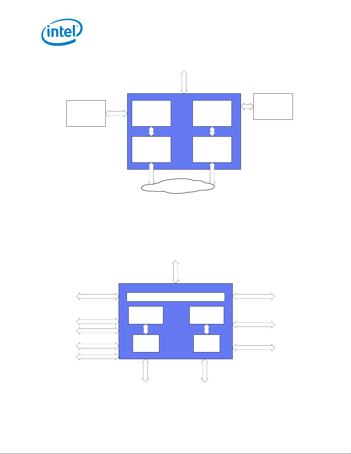
Intel® Ethernet Controller X550 Datasheet—Introduction
MAC(LAN0) MAC(LAN1)
PHY PHY
MDIO
MDIO
Flash
MC/ME
10GBASE‐T_0 10GBASE‐T_1X550
SMBus/
NC‐SI
MC=ManageabilityController
ME=ManageabilityEngine
Network
PCIev3.0(2.5GT/s,5GT/sor8GT/s)x4
PCIev3.0(2.5GT/s,5GT/s)x8
MAC(LAN0) MAC(LAN1)
PHY PHY
10GBASE‐T_0
10GBASE‐T_1
X550
PCIev3.0(2.5GT/s,5GT/sor8GT/s)x4
PCIev3.0(2.5GT/s,5GT/s)x8
SerialFlashI/F
SMBusI/F
NC‐SII/F
HostInterface
DFTI/F
SDP0[3:0]
SDP1[3:0]
LEDs_0
LEDs_1
Figure 1-1. Typical Rack/Pedestal System Configuration
1.3 External Interfaces
Figure 1-2. X550 External Interfaces Diagram
20 333369-004
Page 21

Introduction—Intel
®
Ethernet Controller X550 Datasheet
1.3.1 PCIe Interface
The X550 supports PCIe v3.0 (2.5 GT/s, 5 GT/s or 8 GT/s). See Section 2.2.1 for full pin description and
Section 12.4.5 for interface timing characteristics.
1.3.2 Network Interfaces
Two independent 10GBASE-T interfaces are used to connect the two X550 ports to external devices.
Each 10GBASE-T interface can operate at any of the following speeds:
• 10 Gb/s, 10GBASE-T mode
• 5 Gb/s, NBASE-T mode
• 2.5 Gb/s, NBASE-T mode
• 1 Gb/s, 1000BASE-T mode
• 100 Mb/s, 100BASE-TX mode
• Refer to Section 2.2.2 for full-pin descriptions. For the timing characteristics of those interfaces,
refer to the relevant external specifications listed in Section 12.4.6.
1.3.3 Serial Flash Interface
The X550 uses an external SPI serial interface to a Flash device, also referred to as Non-Volatile
Memory (NVM). The X550 supports serial Flash devices with up to 4 MB of memory.
1.3.4 SMBus Interface
SMBus is an optional interface for pass-through and/or configuration traffic between an external
Manageability Controller (MC) and the X550.
The X550's SMBus interface supports a standard SMBus, up to a frequency of 1 MHz. Refer to
Section 2.2.4 for full-pin descriptions and Section 12.4.4.3 for timing characteristics of this interface.
1.3.5 NC-SI Interface
NC-SI is an optional interface for pass-through traffic to and from an MC. The X550 meets the NC-SI
version 1.0.0 specification.
Refer to Section 2.2.5 for the pin descriptions, and Section 11.6 for NC-SI programming.
333369-004 21
Page 22

Intel® Ethernet Controller X550 Datasheet—Introduction
1.3.6 Software-Definable Pins (SDP) Interface (General-Purpose I/O)
The X550 has four SDP pins per port that can be used for miscellaneous hardware or softwarecontrollable purposes. These pins can each be individually configured to act as either input or output
pins. Via the SDP pins, the X550 can support IEEE1588 auxiliary device connections and other
functionality. For more details on the SDPs see Section 3.5 and the ESDP register (Section 8.2.2.1.4).
1.3.7 LED Interface
The X550 implements four output drivers intended for driving external LED circuits per port. Each of the
four LED outputs can be individually configured to select the particular event, state, or activity, which is
indicated on that output. In addition, each LED can be individually configured for output polarity as well
as for blinking versus non-blinking (steady-state) indications.
The configuration for LED outputs is specified via the LEDCTL register (see Section 8.2.2.1.10). In
addition, the hardware-default configuration for all LED outputs can be specified via an NVM field (see
Section 6.4.7.3), thereby supporting LED displays configured to a particular OEM preference. For more
details on the LEDs see Section 3.6.
1.4 Feature Summary
Tab l e 1 -1 to Ta ble 1-7 list the X550's features in comparison to previous dual-port 10 GbE Ethernet
controllers.
Table 1-1. Network Features
Feature 82599 X540 X550
Compliant with the 10 GbE and 1 GbE Ethernet/802.3ap (KX/KX4)
specification
Compliant with the 10 GbE 802.3ap (KR) specification Y N N
Compliant with XFI/SFI interface Y N N
Compliant with the 1000BASE-BX specification Y N N
Full-duplex operation at all supported speeds Y Y Y
Half-duplex at 100 Mb/s operation N N N
10 GbE/1 GbE/100 Mb/s copper PHYs integrated on-chip N Y Y
802.3az Energy Efficient Ethernet (EEE) support N N Y
Support jumbo frames of up to 15.5 KB Y
MDIO interface Clause 45 Y Y (internally) Y (internally)
Flow Control support: Send/receive pause frames and receive Fifo
thresholds
Statistics for Management and RMON Y Y Y
802.1q VLAN support Y Y Y
SerDes interface for external PHY connection or system
interconnect
YNN
1
YYY
YNN
1
Y
1
Y
22 333369-004
Page 23

Introduction—Intel
®
Ethernet Controller X550 Datasheet
Table 1-1. Network Features (Continued)
Feature 82599 X540 X550
SGMII interface
Double VLAN YYY
1. All the products support full-size 15.5 KB jumbo packets while in a basic mode of operation. When DCB mode is enabled, or security
engines enabled, or virtualization is enabled, or OS2BMC is enabled, then only 9.5 KB jumbo packets are supported. Packets to/
from the MC longer than 2 KB are filtered out.
Y
(100 Mb/s and
1 GbE only)
NN
Table 1-2. Host Interface Features
Feature 82599 X540 X550
PCIe* version (Speed)
Number of lanes x1, x2, x4, x8 x1, x2, x4, x8
64-bit address support for systems using more than 4 GB of
physical memory
Outstanding requests for Tx data buffers 16 16 16
Outstanding requests for Tx descriptors 8 8 8
Outstanding requests for Rx descriptors 8 8 8
Credits for P-H/P-D/NP-H/NP-D (shared for the two ports) 16/16/4/4 16/16/4/4 16/16/4/4
Max Payload Size supported 512 Bytes 512 Bytes 512 Bytes
Max Request Size supported 2 KB 2 KB 2 KB
Link layer retry buffer size (shared for the two ports) 3.4 KB 3.4 KB 3.4 KB
Vital Product Data (VPD) Y Y Y
End to End CRC (ECRC) Y Y Y
TLP Processing Hints (TPH) N N Y
Latency Tolerance Reporting (LTR) N N Y
ID-Based Ordering (IDO) N N Y
Access Control Services (ACS) N Y Y
ASPM optional compliance capability N Y Y
PCIe functions off via pins, while LAN ports are on N Y Y
PCIe v2.0
(5/2.5 GT/s)
YYY
PCIe v2.1
(5/2.5 GT/s)
PCIe v3.0
(8/5/2.5 GT/s)
x1, x4
x8 (For X550-BT2,
x8 available in
Gen 1/2 only)
Table 1-3. Miscellaneous Features
Feature 82599 X540 X550
Serial Flash Interface (SFI) Y Y Y
4-wire SPI EEPROM interface Y N N
Configurable LED operation for software or OEM customization of
LED displays
Protected NVM Space for Private Configuration Y Y Y
Device disable capability Y Y Y
333369-004 23
YYY
Page 24

Intel® Ethernet Controller X550 Datasheet—Introduction
Table 1-3. Miscellaneous Features (Continued)
Feature 82599 X540 X550
Package size 25 mm x 25 mm 25 mm x 25 mm
Embedded thermal sensor N Y Y
Embedded thermal diode N Y Y
Watchdog timer Y Y Y
Time Sync (IEEE 1588) Y Y
Time Stamp in packet N N Y
1. Time sync not supported at 100 Mb/s link speed.
1
25 mm x 25 mm
17 mm x 17 mm
Y
Table 1-4. LAN Functions Features
Feature 82599 X540 X550
Programmable host memory receive buffers Y Y Y
Descriptor ring management hardware for transmit and receive Y Y Y
ACPI register set and power down functionality supporting D0 and
D3 states
Integrated IPsec security engines: AES-GCM 128-bit; AH or ESP
encapsulation; IPv4 and IPv6 (no option or extension headers)
Software-controlled global reset bit (resets everything except the
PCIe configuration registers)
Software-Definable Pins (SDP) (per port) 8 4 4
Four SDP Pins can be configured as general purpose interrupts Y Y Y
Wake on LAN (WoL) Y Y Y
IPv6 Wake-up Filters YYY
Configurable (through NVM) Wake-up Flexible Filters Y Y Y
Default configuration by NVM for all LEDs for pre-driver
functionality
LAN Function Disable capability Y Y Y
Programmable memory transmit buffers 160 KB / port 160 KB / port 160 KB / port
Programmable memory receive buffers 512 KB / port 384 KB / port 384 KB / port
YYY
1024 SA / port 1024 SA / port 1024 SA / port
YYY
YYY
Table 1-5. LAN Performance Features
Feature 82599 X540 X550
TCP/UDP segmentation offload
TSO interleaving for reduced latency Y Y Y
TCP Receive Side Coalescing (RSC) 32 flows / port 32 flows / port 32 flows / port
Data Center Bridging (DCB), IEEE Compliance to:
• Enhanced Transmission Selection (ETS) - 802.1Qaz
• Priority-based Flow Control (PFC) - 802.1Qbb
Rate limit VM Tx traffic per TC (i.e. per TxQ) Y Y Y
IPv6 support for IP/TCP and IP/UDP receive checksum offload Y Y Y
24 333369-004
256 KB in all
modes
Y (up to 8)
Y (up to 8)
256 KB in all
modes
Y (up to 8)
Y (up to 8)
256 KB in all
modes
Y (up to 8)
Y (up to 8)
Page 25

Introduction—Intel
®
Ethernet Controller X550 Datasheet
Table 1-5. LAN Performance Features (Continued)
Feature 82599 X540 X550
Fragmented UDP checksum offload for packet reassembly Y Y Y
FCoE Tx / Rx CRC offload Y Y Y
FCoE transmit segmentation 256 KB 256 KB 256 KB
512 outstanding
Read — Write
FCoE coalescing and direct data placement
Message Signaled Interrupts (MSI) Y Y Y
Message Signaled Interrupts (MSI-X) Y Y Y
Interrupt Throttling Control to limit maximum interrupt rate and
improve CPU use
Rx packet split header Y Y Y
Multiple Rx queues (RSS)
Flow Director Filters: up to 32 KB flows by hash filters or up to 8
KB perfect match filters
Number of Rx queues (per port) 128 128 128
Number of Tx queues (per port) 128 128 128
Low Latency Interrupts (LLI) Y Y N
DCA support YYN
TCP timer interrupts Y Y Y
No snoop YYN
Relax ordering YYY
DMA coalescing N N Y
requests / port
256 buffers per
request
YYY
Y
(multiple modes)Y (multiple modes)Y (multiple modes)
YYY
512 outstanding
Read — Write
requests / port
256 buffers per
request
2048 outstanding
Read — Write
requests / port
1024 buffers per
request
Table 1-6. Virtualization Features
Feature 82599 X540 X550
Support for Virtual Machine Device Queues (VMDq1 and Next
Generation VMDq)
L2 Ethernet MAC Address filters (unicast and multicast) 128 128 128
L2 VLAN filters 64 64 64
PCI-SIG SR IOV Y Y Y
RSS table per VF N N Y
Traffic shaping YYY
Anti-spoof MAC, VLAN MAC, VLAN
Malicious driver protection N N Y
Forwarding modes MAC, VLAN MAC, VLAN MAC, VLAN, E-tag
333369-004 25
64 64 64
MAC, VLAN,
Ethertype
Page 26

Intel® Ethernet Controller X550 Datasheet—Introduction
Table 1-6. Virtualization Features (Continued)
Feature 82599 X540 X550
VEB support
• Multicast and broadcast packet replication
•Packet mirroring
• Packet loopback
VEPA support (on top of VEB support)
• Source pruning N N Y
E-tag filtering support N N Y
Y
Y
Y
Y
Y
Y
Y
Y
Y
Table 1-7. Manageability Features
Feature 82599 X540 X550
Advanced pass-through-compatible management packet transmit/
receive support
SMBus interface to an external MC Y Y Y
New Management Protocol Standards Support (NC-SI) interface to
an external MC
L2 address filters 4 4 4
VLAN L2 filters 8 8 8
Flex L3 port filters 16 16 16
Flexible TCO filters 4 4 1
L3 address filters (IPv4) 4 4 4
L3 address filters (IPv6) 4 4 4
Host-based Application-to-BMC Network Communication patch
(OS2BMC)
Flexible MAC Address N Y Y
MC inventory of LOM device information N Y Y
iSCSI boot configuration parameters via MC N Y Y
MC monitoring N Y Y
NC-SI to iMC NYY
NC-SI arbitration N Y Y
MCTP over SMBus (pass-through and control) N Y (control only) Y
MCTP over PCIe (pass-through and control) N N Y
NC-SI package ID via SDP pins N Y Y
NC-SI Flow control N N Y
YYY
YYY
NYY
26 333369-004
Page 27

Introduction—Intel
®
Ethernet Controller X550 Datasheet
1.5 Overview: New Capabilities Beyond the X540
1.5.1 NBASE-T Support
Support for 2.5GBASE-T and 5GBASE-T is added to the X550.
1.5.2 Filtering Capabilities
1.5.2.1 Flow Director Improvements
Two new modes, based on cloud tenant ID or on MAC, VLAN are added to the X550 to allow support of
the features described below. Also supported is a better definition of the packet which are candidate to
the flow director filtering and the ability to drop candidate packets that do not match any filter.
1.5.2.2 802.1BR Support
The X550 supports the IEEE 802.1BR specification. It allows forwarding to pools based on unicast or
multicast E-tags and allow insertion and removal of the E-tag using a per pool policy.
To allow L2 filtering on top of the E-tag forwarding, the flow director may be configured to MAC, VLAN
filtering and non matching packets may be dropped.
1.5.2.3 VXLAN and NVGRE Support
The X550 supports detection and off-loading of NVGRE and VXLAN packets. It provides transmit and
receive checksum off-load on both inner and outer IP headers and on TCP header. It also allows
forwarding to a specific VM within a tenant using a new flow director mode.
In the regular IP mode of the flow director, VXLAN and NVGRE flows can be differentiated from regular
IP packets and filtering based on the inner IP/L4 header is supported.
1.5.3 IEEE 1588 Improvements
The X550 improves the support for IEEE 1588 by adding the following features:
• Sampling based on a fixed clock, allowing operation independent from the link speed.
• Clock representation is divided to seconds, nanoseconds and sub-nano parts - allowing easier
handling by software.
• Enabling of sub-ns periodic corrections.
• Gradual time adjustment of frequency corrections preventing single large correction. An interrupt is
provided when the adjustment is done.
• Support for two different target times for SDP toggling.
• Each SDP can be associated with any 1588 functionality.
• Allow timestamp to be received in register or embedded in packet.
333369-004 27
Page 28

Intel® Ethernet Controller X550 Datasheet—Introduction
1.5.4 Manageability
1.5.4.1 DMTF MCTP Protocol Over PCIe
The X550 enables reporting and controlling all information exposed in a LOM device via NC-SI using the
MCTP protocol over PCIe in addition to SMBus. The MCTP interface over PCIe is used by the MC to
control the NIC and for pass-through traffic. In addition, the MCTP over SMBus interface can also be
used for pass-through traffic. For more information, refer to Section 11.7.
1.5.4.2 NVM Structures
Management related NVM structures were updated. For further information see Section 6.0.
1.5.4.3 Simplified SMBus TCO Status and Filter Setting
The TCO status in an SMBus received packet was reduced to 8 bytes and most of the information was
removed to keep only the information relevant to the MCs. See Section 11.5.11.2.1.1 for details.
In addition, a generic command was added to enable the setting of most common filtering options
independently of the actual filters implementation. See Section 11.5.11.1.7 and Section 11.5.11.1.8 for
details.
1.5.4.4 Diagnostic Commands
A command was added to the legacy SMBus interface to enable querying the identity of the X550 and
the firmware versions currently running on the X550. See Section 11.5.11.2.6 for details. This
command is the SMBus counterpart of the NC-SI command described in Section 11.6.3.13.2.
1.6 Conventions
1.6.1 Terminology and Acronyms
See Section 16.0, “Glossary and Acronyms”.
1.6.2 Byte Ordering
This section defines the organization of registers and memory transfers, as it relates to information
carried over the network:
• Any register defined in Big Endian notation can be transferred as is to/from Tx and Rx buffers in the
host memory. Big Endian notation is also referred to as being in network order or ordering.
• Any register defined in Little Endian notation must be swapped before it is transferred to/from Tx
and Rx buffers in the host memory. Registers in Little Endian order are referred to being in host
order or ordering.
28 333369-004
Page 29

Introduction—Intel
®
Ethernet Controller X550 Datasheet
Tx and Rx buffers are defined as being in network ordering; they are transferred as is over the network.
Note: Registers not transferred on the wire are defined in Little Endian notation. Registers
transferred on the wire are defined in Big Endian notation, unless specified differently.
1.7 References
The X550 implements features from the following specifications:
IEEE Specifications:
• 10GBASE-T as per the IEEE 802.3an standard.
• 1000BASE-T and 100BASE-TX as per the IEEE standard 802.3-2012 (Ethernet). Incorporates
various IEEE Standards previously published separately. Institute of Electrical and Electronic
Engineers (IEEE).
• NBASE-T as per the IEEE P802.3bz/D1.1 Draft Standard for Ethernet Amendment
• IEEE 1149.6 standard for Boundary Scan (MDI pins excluded)
• IEEE standard 802.3ap, draft D3.2.
• IEEE standard 1149.1, 2001 Edition (JTAG). Institute of Electrical and Electronics Engineers (IEEE).
• IEEE standard 802.1Q for VLAN.
• IEEE 1588 International Standard, Precision clock synchronization protocol for networked
measurement and control systems, 2004-09.
• IEEE P802.1AE/D5.1, Media Access Control (MAC) Security, January 19, 2006.
• IEEE 802.3az Energy Efficient Ethernet Amendment to IEEE 802.3, October 2010.
• IEEE standard 802.1BR D3.3 - February 20, 2012.
• IEEE 802.Qbg - Amendment 21: Edge Virtual Bridging. 5 July 2012.
PCI-SIG Specifications:
• PCI Express* 2.0 Card Electromechanical Specification
• PCI Express 3.0 Base specification
• PCI Bus Power Management Interface Specification, Rev. 1.2, March 2004.
• PICMG3.1 Ethernet/Fibre Channel Over PICMG 3.0 Draft Specification January 14, 2003 Version
D1.0.
• Single Root I/O Virtualization and Sharing, Revision 1.1, September 8, 2009.
IETF Specifications:
• IPv4 specification (RFC 791)
• IPv6 specification (RFC 2460)
• TCP specification (RFC 793)
• UDP specification (RFC 768)
• ARP specification (RFC 826)
333369-004 29
Page 30

Intel® Ethernet Controller X550 Datasheet—Introduction
IETF Drafts:
• VXLAN — A Framework for Overlaying Virtualized Layer 2 Networks over Layer 3 Networks: draftmahalingam-dutt-dcops-vxlan-03. February 22, 2013
• NVGRE — Network Virtualization using Generic Routing Encapsulation: draft-sridharanvirtualization-nvgre-02. February 24, 2013
Manageability Documents:
• DSP0222 — DMTF Network Controller Sideband Interface (NC-SI) Specification rev 1.0.1, January
2013
• DSP0236 — DMTF Management Component Transport Protocol (MCTP) Base Specification, rev
1.2.0, January 2013
2
• DSP0237 — DMTF Management Component Transport Protocol (MCTP) SMBus/I
C Transport
Binding Specification, rev 1.0.0, July 2009
• DSP0238 — DMTF Management Component Transport Protocol (MCTP) PCIe VDM Transport Binding
Specification, rev 1.0.1, December 2009
• DSP0239 — DMTF Management Component Transport Protocol (MCTP) IDs and Codes, rev 1.2.0,
August 2012
• DSP0261 — DMTF NC-SI Over MCTP Binding Specification - Work in Progress,
• System Management Bus (SMBus) Specification, SBS Implementers Forum, Ver. 2.0, August 2000
2
• UM10204 — I
C-bus specification and user manual Rev. 5 — 9 October 2012
Proxy Documents:
• proxZZZy™ for sleeping hosts, February 2010 (ECMA-393)
Other:
• Advanced Configuration and Power Interface Specification, Rev 2.0b, October 2002
• EUI-64 specification, http://standards.ieee.org/regauth/oui/tutorials/EUI64.html.
• Definition for new PAUSE function, Rev. 1.2, 12/26/2006.
• GCM spec — McGrew, D. and J. Viega, “The Galois/Counter Mode of Operation (GCM)”, Submission
to NIST, January 2004.
http://csrc.nist.gov/CryptoToolkit/modes/proposedmodes/gcm/gcm-spec.pdf
• FRAMING AND SIGNALING-2 (FC-FS-2) Rev 1.00
• Fibre Channel over Ethernet Draft Presented at the T11 on May 2007
• Per Priority Flow Control (by Cisco Systems) — Definition for new PAUSE function, Rev 1.2, EDCS472530
• NBASE-T Physical Layer Specification version 1.1
30 333369-004
Page 31

Introduction—Intel
®
Ethernet Controller X550 Datasheet
1.8 Architecture and Basic Operation
1.8.1 Transmit (Tx) Data Flow
Tx data flow provides a high-level description of all data/control transformation steps needed for
sending Ethernet packets over the wire.
Table 1-8. Tx Data Flow
Step Description
1 The software device driver creates a descriptor ring and configures one of the X550’s transmit queues with the
2 The software device driver is requested by the TCP/IP stack to transmit a packet, it gets the packet data within
3 The software device driver initializes the descriptor(s) that point to the data buffer(s) and have additional control
4 The software device driver updates the appropriate Queue Tail Pointer (TDT).
5 The X550’s DMA senses a change of a specific TDT and as a result sends a PCIe request to fetch the descriptor(s)
6 The descriptor(s) content is received in a PCIe read completion and is written to the appropriate location in the
7 The DMA fetches the next descriptor and processes its content. As a result, the DMA sends PCIe requests to fetch
8 The packet data is received from PCIe completions and passes through the transmit DMA that performs all
9 While the packet is passing through the DMA, it is stored into the transmit FIFO.
10 The transmit switch arbitrates between host and management packets and eventually forwards the packet to the
11 The security module optionally encrypts the packet and authenticates it using IPsec and passes the packet to the
12 The MAC appends the L2 CRC to the packet and delivers the packet to the integrated PHY.
13 The PHY performs the PCS encoding, scrambling, Low-Density Parity Check (LDPC) encoding, and the other
14 When all the PCIe completions for a given packet are complete, the DMA updates the appropriate descriptor(s).
15 The descriptors are written back to host memory using PCIe posted writes. The head pointer is updated in host
16 An interrupt is generated to notify the software device driver that the specific packet has been read to the X550
address location, length, head, and tail pointers of the ring (one of 128 available Tx queues).
one or more data buffers.
parameters that describes the needed hardware functionality. The host places that descriptor in the correct
location in the appropriate Tx ring.
from host memory.
descriptor queue.
the packet data from system memory.
programmed data manipulations (various CPU offloading tasks as checksum offload, TSO offload, etc.) on the
packet data on the fly.
After the entire packet is stored in the transmit FIFO, it is then forwarded to transmit switch module.
security module.
MAC.
manipulations required to deliver the packet over the copper wires at the selected speed.
memory as well if the X550 is configured to do so.
and the driver can then release the buffer(s).
333369-004 31
Page 32

Intel® Ethernet Controller X550 Datasheet—Introduction
1.8.2 Receive (Rx) Data Flow
Rx data flow provides a high-level description of all data/control transformation steps needed for
receiving Ethernet packets.
Table 1-9. Rx Data Flow
Step Description
1 The software device driver creates a descriptor ring and configures one of the X550’s receive queues with the
2 The software device driver initializes descriptor(s) that point to empty data buffer(s). The software device driver
3 The software device driver updates the appropriate Queue Tail Pointer (RDT).
4 A packet enters the PHY through the copper wires.
5 The PHY performs the required manipulations on the incoming signal such as LDPC decoding, de-scrambling, PCS
6 The PHY delivers the packet to the Rx MAC.
7 The MAC forwards the packet to the security block.
8 If the packet is identified as a IPsec packet, it is decrypted.
9 If the packet matches the pre-programmed criteria of the Rx filtering, it is forwarded to an Rx FIFO.
10 The receive DMA fetches the next descriptor from the appropriate host memory ring to be used for the next
11 After the entire packet is placed into an Rx FIFO, the receive DMA posts the packet data to the location indicated
12 When the packet is placed into host memory, the receive DMA updates all the descriptor(s) that were used by the
13 The receive DMA writes back the descriptor content along with status bits that indicate the packet information
14 The X550 initiates an interrupt to the software device driver to indicate that a new received packet is ready in host
15 The software device driver reads the packet data and sends it to the TCP/IP stack for further processing. The
address location, length, head, and tail pointers of the ring (one of 128 available Rx queues).
places these descriptor(s) in the correct location at the appropriate Rx ring.
decoding, etc.
received packet.
by the descriptor through the PCIe interface.
If the packet size is greater than the buffer size, more descriptor(s) are fetched and their buffers are used for the
received packet.
packet data.
including what offloads were done on that packet.
memory.
software device driver releases the associated buffer(s) and descriptor(s) once they are no longer in use.
32 333369-004
Page 33

Pin Interface—Intel
®
Ethernet Controller X550 Datasheet
2.0 Pin Interface
2.1 Signal Type Definition
Signal Definition DC Specification
In Standard 3.3 V I/O buffer, functions as input-only signal.
Out (O) Standard 3.3 V I/O buffer, functions as output-only signal.
T/s Tri-state is a 3.3 V bi-directional, tri-state input/output pin.
O/d Open drain enables multiple devices to share as a wire-OR. Section 12.4.2
A-in Analog input signals. Section 12.4.5 and Section 12.4.6
A-out Analog output signals. Section 12.4.5 and Section 12.4.6
A-Inout Bi-directional analog signals.
B Input BIAS.
NCSI-in NC-SI 3.3 V input signal. Section 12.4.3
NCSI-out NC-SI 3.3 V output signal. Section 12.4.3
In-1p2 1.2 V input-only signal. 3.3 V tolerance.
In-Only Standard 3.3 V buffer input-only signal.
Out-Only Standard 3.3 V buffer output-only signal.
LVDS-O Low voltage differential signal - output.
Pup Pull up.
Pdn Pull down.
333369-004 33
Page 34

2.2 Pin Assignments
2.2.1 PCIe
See AC/DC specifications in Section 12.4.5.
Intel® Ethernet Controller X550 Datasheet—Pin Interface
Pin Name
PET_0_p
PET_0_n
PET_1_p
PET_1_n
PET_2_p
PET_2_n
PET_3_p
PET_3_n
PET_4_p
PET_4_n
PET_5_p
PET_5_n
PET_6_p
PET_6_n
PET_7_p
PET_7_n
PER_0_p
PER_0_n
PER_1_p
PER_1_n
PER_2_p
PER_2_n
PER_3_p
PER_3_n
PER_4_p
PER_4_n
PER_5_p
PER_5_n
PER_6_p
PER_6_n
PER_7_p
PER_7_n
PE_CLK_p
PE_CLK_n
Ball #
(X550-AT2)
T5
T6
T8
T9
T11
T12
T14
T15
N/A
N/A
N/A
N/A
P6
P7
P9
P10
P12
P13
P15
P16
N/A
N/A
N/A
N/A
N4
P4
Ball #
(X550-BT2)
AC3
AD3
AC4
AD4
AC9
AD9
AC10
AD10
AC15
AD15
AC16
AD16
AC21
AD21
AC22
AD22
AB2
AB1
AD6
AC6
AD7
AC7
AD12
AC12
AD13
AC13
AD18
AC18
AD19
AC19
AB23
AB24
Y2
Y1
Type
A-Out
A-Out
A-Out
A-Out
A-Out
A-Out
A-Out
A-Out
A-In
A-In
A-In
A-In
A-In
A-In
A-In
A-In
A-In
Internal
Pup/Pdn
External
Pup/Pdn
Name and Function
PCIe Serial Data Output: A serial differential
output pair running at 8 Gb/s, 5 Gb/s, or
2.5 Gb/s. This output carries both data and an
embedded 8 GHz or 5 GHz or 2.5 GHz clock that
is recovered along with data at the receiving
end.
PCIe Serial Data Output: A serial differential
output pair running at 5 Gb/s or 2.5 Gb/s. This
output carries both data and an embedded
5 GHz or 2.5 GHz clock that is recovered along
with data at the receiving end.
Available only in the X550-BT2.
PCIe Serial Data Input: A serial differential
input pair running at 8 Gb/s, 5 Gb/s, or 2.5 Gb/
s. This input carries both data and an embedded
8GHz, 5GHz, or 2.5GHz clock that is
recovered along with data at the receiving end.
PCIe Serial Data Input: A serial differential
input pair running at 5 Gb/s or 2.5 Gb/s. This
input carries both data and an embedded 5 GHz
or 2.5 GHz clock that is recovered along with
data at the receiving end.
Available only in the X550-BT2.
PCIe Differential Reference Clock In (a 100
MHz differential clock input): This clock is
used as the reference clock for the PCIe Tx/Rx
circuitry and by the PCIe core PLL to generate
clocks for the PCIe core logic.
34 333369-004
Page 35

Pin Interface—Intel
®
Ethernet Controller X550 Datasheet
Pin Name
PE_RBIAS T3 Y4 A-Inout
PE_RSENSE R3 Y5 A-Inout
PE_WAKE_N L3 W1 O/d Pup
PE_RST_N M3 W2 In Pup
1. Pup value should be considered as 10 K.
Ball #
(X550-AT2)
Ball #
(X550-BT2)
Type
Internal
Pup/Pdn
External
Pup/Pdn
2.2.2 MDI
See AC/DC specifications in Section 12.4.6.
Pin Name
MDI0_0_p A2 A3 A-Inout
MDI0_0_n B2 B3 A-Inout
MDI0_1_p A3 A5 A-Inout
MDI0_1_n B3 B5 A-Inout
MDI0_2_p A5 A7 A-Inout
MDI0_2_n B5 B7 A-Inout
MDI0_3_p A6 A9 A-Inout
MDI0_3_n B6 B9 A-Inout
MDI0_4_p A8 A11 A-Inout
MDI0_4_n B8 B11 A-Inout
MDI1_0_p B16 A22 A-Inout
Ball #
(X550-AT2)
Ball #
(X550-BT2)
Type
Internal
Pup/Pdn
External
Pup/Pdn
Name and Function
BIAS: A 4.75 K ±0.1% resistor should be
connected between RBIAS and RSENSE pins.
Connect resistor as close as possible to the chip.
Resistor is used for internal impedance
compensation and BIAS current generation
circuitry.
Wake: Pulled low to indicate that a Power
Management Event (PME) is pending and the
1
PCIe link should be restored. Defined in the
PCIe specifications.
Power and Clock Good Indication: Indicates
that power and the PCIe reference clock are
within specified values. Defined in the PCIe
specifications. Also called PCIe Reset.
Name and Function
Port 0 pair A+ of the Line Interface:
Connects to the Pair A+ input of the
transformer. On reset, set to high impedance.
Port 0 pair A- of the Line Interface:
Connects to the Pair A- input of the transformer.
On reset, set to high impedance.
Port 0 pair B+ of the Line Interface:
Connects to the Pair B+ input of the
transformer. On reset, set to high impedance.
Port 0 pair B- of the Line Interface:
Connects to the Pair B- input of the transformer.
On reset, set to high impedance.
Port 0 pair C+ of the Line Interface:
Connects to the Pair C+ input of the
transformer. On reset, set to high impedance.
Port 0 pair C- of the Line Interface:
Connects to the Pair C- input of the transformer.
On reset, set to high impedance.
Port 0 pair D+ of the Line Interface:
Connects to the Pair D+ input of the
transformer. On reset, set to high impedance.
Port 0 pair D- of the Line Interface:
Connects to the Pair D- input of the transformer.
On reset, set to high impedance.
Port 0 Analog Test+: Connects to the pair E+
input of the transformer.
Port 0 Analog Test-: Connects to the pair Einput of the transformer.
Port 1 pair A+ of the Line Interface:
Connects to the Pair A+ input of the
transformer. On reset, set to high impedance.
333369-004 35
Page 36

Intel® Ethernet Controller X550 Datasheet—Pin Interface
Pin Name
MDI1_0_n C16 B22 A-Inout
MDI1_1_p A14 A20 A-Inout
MDI1_1_n B14 B20 A-Inout
MDI1_2_p A12 A18 A-Inout
MDI1_2_n B12 B18 A-Inout
MDI1_3_p A11 A16 A-Inout
MDI1_3_n B11 B16 A-Inout
MDI1_4_p A9 A14 A-Inout
MDI1_4_n B9 B14 A-Inout
BG_REXT B15 D12 A-Inout
XTAL_I D16 D23 A-In Positive 50.0 MHz crystal oscillator input.
XTAL_O E16 D24 A-Out Positive 50.0 MHz crystal oscillator output.
RSVDF5_VSS N/A F5 In
Ball #
(X550-AT2)
Ball #
(X550-BT2)
Type
Internal
Pup/Pdn
External
Pup/Pdn
Name and Function
Port 1 pair A- of the Line Interface:
Connects to the Pair A- input of the transformer.
On reset, set to high impedance.
Port 1 pair B+ of the Line Interface:
Connects to the Pair B+ input of the
transformer. On reset, set to high impedance.
Port 1 pair B- of the Line Interface:
Connects to the Pair B- input of the transformer.
On reset, set to high impedance.
Port 1 pair C+ of the Line Interface:
Connects to the Pair C+ input of the
transformer. On reset, set to high impedance.
Port 1 pair C- of the Line Interface:
Connects to the Pair C- input of the transformer.
On reset, set to high impedance.
Port 1 pair D+ of the Line Interface:
Connects to the Pair D+ input of the
transformer. On reset, set to high impedance.
Port 1 pair D- of the Line Interface: Connect
to the pair D- input of the transformer. On reset,
set to high impedance.
Port 1 Analog Test+: Connects to the pair E+
input of the transformer.
Port 1 Analog Test-: Connects to the pair Einput of the transformer.
Connection point for the band-gap reference
resistor. Should be a precision 1% 2 K resistor
tied to ground.
2.2.3 Serial Flash
See AC/DC specifications in Section 12.4.4.4.
Pin Name
FLSH_SI K3 K2 Out Pup
FLSH_SO J3 K1 In
FLSH_SCK L1 J1 Out
FLSH_CE_N L2 J2 Out Pup
1. Pup value should be considered as 3.3 K.
36 333369-004
Ball #
(X550-AT2)
Ball #
(X550-BT2)
Type
Internal
Pup/Pdn
External
Pup/Pdn
1
Name and Function
Flash Serial Output: Serial data output to the
Flash (used as ENCRYPTION_EN strap in
X550-AT2).
Flash Serial Input: Serial data input from the
Flash.
Flash serial clock: Operates at the maximum
frequency of 25 MHz.
This pin acts as a JTAG_DIS strap.
Flash Chip Select Output
Page 37

Pin Interface—Intel
®
Ethernet Controller X550 Datasheet
2.2.4 SMBus
See the AC/DC specifications in Section 12.4.4.3.
Pin Name
SMBCLK F3 L2 O/d Pup
SMBD F2 L1 O/d Pup
SMBALRT_N F1 M2 O/d Pup
1. Pup value should be considered as 10 K.
Ball #
(X550-AT2)
Ball #
(X550-BT2)
Type
Internal
Pup/Pdn
External
Pup/Pdn
1
1
1
Name and Function
SMBus Clock: One clock pulse is generated for
each data bit transferred.
SMBus Data: Stable during the high period of
the clock (unless it is a start or stop condition).
SMBus Alert: Acts as an interrupt pin of a slave
device on the SMBus.
Note: If the SMBus is disconnected, use the external pull-up value listed.
2.2.5 NC-SI
See AC specifications in Section 12.4.4.5.
Pin Name
NCSI_CLK_IN D2 G2 NCSI-In Pdn
NCSI_TX_EN B1 G4 NCSI-In Pdn
NCSI_TXD0
NCSI_TXD1
NCSI_CRS_DV E3 H1 NCSI-Out Pup
NSCI_RXD0
NCSI_RXD1
NCSI_ARB_IN C1 F1 NCSI-In Pdn NC-SI Arbitration In
NCSI_ARB_OUT D1 F2 NCSI-Out NC-SI Arbitration Out
1. Pdn or Pup value should be considered as 10 K.
2. Should be pulled down if NC-SI interface is disabled.
3. Should be pulled up if NC-SI interface is disabled or if set to multi drop configuration.
Ball #
(X550-AT2)
D3
D4
E1
E2
Ball #
(X550-BT2)
H2
G3
H3
G1
Type
NCSI-In Pup or Pdn
NCSI-Out Pup
Internal
Pup/Pdn
External
Pup/Pdn
2
3
3
1
NC-SI Reference Clock Input:
Synchronous clock reference for
receive, transmit, and control interface.
It is a 50 MHz clock ±100 ppm.
MC Transmit Enable: Indicates that
received data from MC is valid.
MC Transmit Data: Data signals from
2
the MC to the X550.
Carrier Sense/Receive Data Valid
(CRS/DV) to MC: Indicates that the
data transmitted from the X550 to MC
is valid.
MC Receive Data: Data signals from
the X550 to the MC.
Name and Function
333369-004 37
Page 38

Intel® Ethernet Controller X550 Datasheet—Pin Interface
2.2.6 Software Defined Pins (SDPs)
See AC specifications in Section 12.4.4.1.
See Section 3.5 for more details on configurable SDPs.
Pin Name
SDP0_0
SDP0_1
SDP0_2
SDP0_3
SDP1_0
SDP1_1
SDP1_2
SDP1_3
Ball #
(X550-AT2)
H1
G1
H2
G2
H16
G16
H15
G15
Ball #
(X550-BT2)
R4
P3
T4
R3
T21
T22
U21
U22
Type
T/s
T/s
Internal
Pup/Pdn
2.2.7 LEDs
See AC specifications in Section 12.4.4.1.
Pin Name
LED0_0 K1 H4 Out Pdn
LED0_1 J1 J3 Out Pdn
LED0_2 K2 J4 Out Pdn
LED0_3 J2 K4 Out Pdn
LED1_0 K16 J21 Out Pdn
LED1_1 J16 J22 Out Pdn
LED1_2 K15 K21 Out Pdn
LED1_3 J15 K22 Out Pdn
Ball #
(X550-AT2)
Ball #
(X550-BT2)
Type
Internal
Pup/Pdn
Pdn
Pdn
Pdn
Pdn
Pdn
Pdn
Pdn
Pdn
External
Pup/Pdn
External
Pup/Pdn
Name and Function
General Purpose SDPs — 3.3 V I/Os for
Function 0: Can be used to support IEEE1588
auxiliary devices.
Input for external interrupts, PCIe function
disablement, etc.
See Section 3.5 for possible usages of the pins.
General Purpose SDPs — 3.3 V I/Os for
Function 1: Can be used to support IEEE1588
auxiliary devices.
Input for external interrupts, PCIe function
disablement, etc.
See Section 3.5 for possible usages of the pins.
Name and Function
Port 0 LED0: Programmable LED. By default,
indicates link up.
Port 0 LED1: Programmable LED. By default,
indicates 10 Gb/s link.
Port 0 LED2: Programmable LED. By default,
indicates link/activity.
Port 0 LED3: Programmable LED. By default,
indicates 1 Gb/s link.
Port 1 LED0: Programmable LED. By default,
indicates link up.
Port 1 LED1: Programmable LED. By default,
indicates 10 Gb/s link.
Port 1 LED2: Programmable LED. By default,
indicates link/activity.
Port 1 LED3: Programmable LED. By default,
indicates 1 Gb/s link.
38 333369-004
Page 39

Pin Interface—Intel
®
Ethernet Controller X550 Datasheet
2.2.8 RSVD and No-Connect Pins
Connecting RSVD pins based on naming convention:
• NC — Pin is not connected in the package.
• RSVD_NC — Reserved pin. Should be left unconnected.
• RSVD_VSS — Reserved pin. Should be connected to GND.
• RSVD_VCC — Reserved pin. Should be connected to VCC3P3.
Pin Name
RSVDD14_NC N/A D14 A-Inout Reserved/No-connect pin.
RSVDG21_NC
RSVDG22_NC
RSVDL4_NC
RSVDL3_NC
RSVDM4_NC
RSVDM3_NC
RSVDN4_NC
RSVDN3_NC
RSVDN2_NC
RSVDP4_NC
RSVDL22_NC
RSVDL21_NC
RSVDM22_NC
RSVDM21_NC
RSVDN22_NC
RSVDN21_NC
RSVDP22_NC
RSVDP21_NC
RSVDT23_VSS
RSVDT24_VSS
RSVDP23_NC
RSVDP24_VSS
RSVDL15_VSS
RSVDL16_VSS
RSVDR22_NC N/A R22 Out Reserved/No-connect pin.
RSVDAA6_NC
RSVDAA8_NC
RSVDAA10_NC
RSVDAA14_NC
RSVDAA16_NC
RSVDAA18_NC
RSVDK3_NC
RSVDM24_NC
RSVDT2_NC
RSVDV21_NC
RSVDY21_NC
RSVDG11_NC N/A G11 PWR Reserved/No-connect pin.
Ball #
(X550-AT2)
N/A
N/A
N/A
L15
L16
N/A
Ball #
(X550-BT2)
G21
G22
L4
L3
M4
M3
N4
N3
N2
P4
L22
L21
M22
M21
N22
N21
P22
P21
T23
T24
P23
P24
N/A
AA6
AA8
AA10
AA14
AA16
AA18
K3
M24
T2
V21
Y21
Type Name and Function
A-Inout
A-Inout
Out
Out
Out
Out
Out
Out
Out
Out
Out
Out
Out
Out
Out
Out
Out
Out
Inout
Inout
Inout
Inout
Inout
Inout
Reserved/No-connect pins.
Reserved/No-connect pins.
Reserved VSS pins.
Reserved/No-connect pins.
Reserved/No-connect pins.
333369-004 39
Page 40

Intel® Ethernet Controller X550 Datasheet—Pin Interface
Pin Name
RSVDU3_NC
RSVDR21_NC
RSVDU2_NC
RSVDT3_NC
RSVDV24_NC
RSVDU24_NC
RSVDU23_NC
RSVDV23_NC
RSVDC1_NC
RSVDD1_NC
RSVDE1_NC
RSVDE23_NC
RSVDE24_NC
RSVDF24_NC
RSVDG24_VSS
RSVDH22_VSS
RSVDY20_NC
RSVDN24_NC
RSVDW24_NC
RSVDL23_NC N/A L23 O/d Reserved/No-connect pin.
RSVDJ23_VSS N/A J23 In-Only Reserved VSS pin.
RSVDJ24_VSS N/A J24 In Reserved VSS pin.
RSVDH24_VSS N/A H24 In Reserved VSS pin.
RSVDG23_VSS N/A G23 In-Only Reserved VSS pin.
RSVDAD1_VSS N/A AD1 In Reserved VSS pin.
RSVDD13_NC
RSVDC13_NC
RSVDC11_NC
RSVDD11_NC
RSVDA1_NC
RSVDA24_NC
RSVDAD24_NC
RSVDT1_NC
RSVDU1_NC
RSVDN13_NC
RSVDU4_NC
RSVDR24_NC
RSVDR23_NC
RSVDN1_NC
RSVDP1_NC
RSVDR1_NC
RSVDM23_NC
RSVDN23_NC
RSVDL14_NC
RSVDM14_NC
RSVDV4_NC
RSVDV3_NC
RSVDT1_NC
RSVDR1_NC
Ball #
(X550-AT2)
N/A
N/A
N/A
N/A
N/A
N/A
N/A
L14
M14
N/A
T1
R1
Ball #
(X550-BT2)
U3
R21
U2
T3
V24
U24
U23
V23
C1
D1
E1
E23
E24
F24
G24
H22
Y20
N24
W24
D13
C13
C11
D11
A1
A24
AD24
T1
U1
N13
U4
R24
R23
N1
P1
R1
M23
N23
N/A
V4
V3
N/A A-Out Reserved/No-connect pins.
Type Name and Function
T/s
T/s
T/s
T/s
Reserved/No-connect pins.
T/s
T/s
T/s
T/s
Reserved/No-connect pins.
Reserved/No-connect pins.
A-Inout
A-Inout
A-Out
A-Out
In-Only
In-Only
In-Only
PWR-O
PWR-O
PWR-O
PWR-O
LVDS-O
LVDS-O
Out-Only
Inout
Out
Inout
Out
Inout
Out
A-Out Reserved/No-connect pins.
Reserved/No-connect pins.
Reserved/No-connect pins.
Reserved/No-connect pins.
Reserved/No-connect pins.
Reserved/No-connect pins.
40 333369-004
Page 41

Pin Interface—Intel
®
Ethernet Controller X550 Datasheet
Pin Name
RSVDV1_NC
RSVDV2_NC
RSVDR2_NC
RSVDP2_NC
Ball #
(X550-AT2)
N/A
R2
P2
Ball #
(X550-BT2)
V1
V2
N/A A-Out Reserved/No-connect pins.
Type Name and Function
A-Out Reserved/No-connect pins.
2.2.8.1 Pin Differences in the X550-AT Single Port Device
NC = Pin is not connected in the package.
Name Ball # (X550-AT2) Connection (X550-AT)
MDI1_0_p B16 NC
MDI1_0_n C16 NC
MDI1_1_p A14 NC
MDI1_1_n B14 NC
MDI1_2_p A12 NC
MDI1_2_n B12 NC
MDI1_3_p A11 NC
MDI1_3_n B11 NC
MDI1_4_p A9 NC
MDI1_4_n B9 NC
LAN1_DIS_N M16 NC
For additional information on these pins in the X550-AT2, see Section 2.2.2.
2.2.9 Miscellaneous
See AC/DC specifications in Section 12.4.4.1.
Pin Name
LAN_PWR_GOOD N/A L24 In Pup Pup
BYPASS_POR N/A H23 In Pdn Pdn
AUX_PWR H3 P2 In Note
MAIN_PWR_OK G3 R2 In Note
Ball #
(X550-AT2)
Ball #
(X550-BT2)
Type
Internal
Pup/Pdn
External
Pup/Pdn
1
2
3
4
LAN Power Good: A 3.3 V input signal. A
transition from low to high initializes the
X550 into operation. If not used
(BYPASS_POR = 0b), an internal Power-onReset (POR) circuit triggers the X550 power
up.
Bypass POR
Auxiliary Power Available: When set,
indicates that auxiliary power is available
and the X550 should support D3
state if enabled to do so. This pin is latched
at the rising edge of LAN_PWR_GOOD.
Main Power Good: Indicates that platform
main power is up. Must be connected
externally.
Name and Function
COLD
power
333369-004 41
Page 42

Intel® Ethernet Controller X550 Datasheet—Pin Interface
Pin Name
LAN1_DIS_N
Ball #
(X550-AT2)
M16
(Strap)
Ball #
(X550-BT2)
K24 In
Type
5
Internal
Pup/Pdn
Pup Pup
External
Pup/Pdn
1
Name and Function
LAN 1 Disable: This pin is a strapping pin
latched at the rising edge of
LAN_PWR_GOOD or PE_RST_N or In-Band
PCIe Reset. If this pin is not connected or
driven high during initialization, LAN 1 is
enabled. If this pin is driven low during
initialization, LAN 1 port is disabled.
LAN 0 Disable: This pin is a strapping
option pin latched at the rising edge of
LAN0_DIS_N
M15
(Strap)
K23 In
5
Pup Pup
LAN_PWR_GOOD or PE_RST_N or In-Band
1
PCIe Reset. If this pin is not connected or
driven high during initialization, LAN 0 is
enabled. If this pin is driven low during
initialization, LAN 0 port is disabled.
Strap on
ENCRYPTION_EN
FLSH_SI
M1 In Pup Pdn/Pup
(K3)
THERM_D0_P
THERM_D0_N
1. Pup value should be considered as 1 K.
2. Pdn value should be considered as 1 K.
3. Connect AUX_PWR signal to Pup if AUX power is available. Connect Pdn if AUX power is not available. Pup/Pdn value should be
considered as 1 K.
4. Connect MAIN_PWR_OK signal to Main Power through Pup resistor. Pup value should be considered as 10 K.
C3
C2
F4
F3
A-Inout
A-Inout
Encryption Enable: Enable/disable for the
internal IPsec engines.
1
When pulled up, encryption features are
enabled.
Thermal Diode Reference: Can be used
to measure on-die temperature.
5. For the X550-AT and X550-AT2, this pin is input during PCIe_RST_N assertion only, and is output after that.
2.2.10 JTAG
See AC specifications in Section 12.4.4.2.
Pin Name
Ball #
(X550-AT2)
JTCK F16 Y22 In-Only Pup Pdn
JTDI F14 W22 In-Only Pup Pup
JTDO F15 V22 Out Pup
JTMS G14 W21 In-Only Pup Pup
JTRST_N H14 W23 In-Only Pup Pdn
1. Pdn value should be considered as 470 .
2. Pup value should be considered as 10 K.
3. Pup value should be considered as 3.3 K
Note: If the JTAG is disconnected, use the external pull-up or pull-down values listed.
Ball #
(X550-BT2)
Type
Internal
Pup/Pdn
External
Pup/Pdn
1
2
3
2
1
Name and Function
JTAG Clock Input
JTAG Data Input
JTAG Data Output
JTAG TMS Input
JTAG Reset Input: Active low reset for the
JTAG port.
42 333369-004
Page 43

Pin Interface—Intel
®
Ethernet Controller X550 Datasheet
2.2.11 Power Supplies
See AC specifications in Section 12.3.1.
Pin Name Ball # (X550-AT2) Ball # (X550-BT2) Type Name and Function
RSVDH21_VSS N/A H21 PWR Reserved power pin.
RSVDJ14_VSS J14 N/A PWR Reserved power pin.
B1, B2, D2, E2, C3, D3, B4, E4,
C5, D5, B6, E6, C7, D7, B8, E8,
C9, D9, B10, E10, B12, E12, B13,
C14, E14, B15, D15, C16, E16,
B17, D17, C18, E18, B19, D19,
A1, A4, A7, A10, A13, A15, A16,
VSS
VSS
VSS
NC N/A
VCC0P83
VCC1P2A M1, M2, N1, N2 V6, W5 PWR_ALG 1.2 V
VCC1P2 E4, E6, E8 D10, D4, D8, E11, E7, E9, D6, E5 PWR_ALG 1.2 V
VCC1P2 E10, E12, E14
B4, B7, B10, B13, C5, C7, C9,
C11, C13, C15, D6, D8, D10, D12,
D14, E5, E13, E15
N6, N7, N9, N10, N12, N13, N15,
N16, P3, P5, P8, P11, P14, R4, R5,
R6, R7, R8, R9, R10, R11, R12,
R13, R14, R15, R16, T2, T4, T7,
F4, F6, F8, F10,F12, G5, G7, G9,
G11, G13, H4, H6, H8, H10, H12,
J5, J7, J9, J11, J13, K4, K6, K8,
K10, K12, K14, L5, L7, L9, L11,
F5, F7, F9, F11, F13, G4, G6, G8,
G10, G12, H5, H7, H9, H11, H13,
J4, J6, J8, J10, J12, K5, K7, K9,
K11, K13, L6, L8, L10, L12, M5,
T10, T13, T16
M6, M8, M10, M12
M7, M9, M11
C20, E20, B21, D21, F21, C22,
D22, E22, F22, B23, F23, B24, L6,
L8, L10, L12, L14, L16, L18, L20,
F6, F7, F8, F9, F10, F11, F12, F13,
F14, F15, F16, F17, F18, F19, F20,
G6, G8, G10, G12, G14, G16,
G18, G20, H5, H7, H9, H11, H13,
H15, H17, H19, J6, J8, J10, J12,
J14, J16, J18, J20, K5, K7, K9,
K11, K13, K15, K17, K19
U6, V5, AA1, AC1, AA2, AC2, AD2,
W3, W4, W6, Y3, AA3, AA4, AB4,
AA5, AC5, AD5, AB6, Y7, AA7,
AB7, AC8, AD8, Y9, AA9, AB9,
AB10, Y11, AA11, AC11, AD11,
AA12, AB12, Y13, AA13, AB13,
AC14, AD14, Y15, AA15, AB15,
AB16, Y17, AA17, AC17, AD17,
AB18, Y19, AA19, AB19, AA20,
AC20, AD20, AA21, AB21, AA22,
AA23, AA24, AC23, AD23, AC24
M5, P5, T5, N6, R6, M7, P7, T7,
V7, N8, R8, U8, W8, M9, P9, T9,
V9, N10, R10, U10, W10, M11,
P11, T11, V11, N12, R12, U12,
W12, M13, P13, T13, V13, N14,
R14, U14, W14, M15, P15, T15,
V15, N16, R16, U16, W16, M17,
P17, T17, V17, N18, R18, U18,
W18, M19, P19, T19, V19, J20,
N20, R20, U20, W20, Y23, Y24
G5, G7, G9, G15, G17, G19, H6,
H8, H10, H12, H14, H16, H18,
H20, J5, J7, J9, J11, J15, J17, J19,
K6, K8, K10, K12, K14, K16, K18,
K20, L7, L9, L11, L13, L15, L17,
N7, R7, U7, W7, M8, P8, T8, V8,
N9, R9, U9, W9, M10,M12, P10,
T10, V10, N11, R11, U11, W11,
P12, T12, V12, J13, R13, U13,
W13, M14, P14, T14, V14, N15,
R15, U15, W15, M16, P16, T16,
V16, N17, R17, U17, W17, M18,
E19, D20, D16, D18, E13, E15,
L19
P18, T18, V18
E17
PWR_ALG 1.2 V ground.
PWR_ALG Ground for PCIe.
PWR Ground
No-connect pins.
PWR 0.83 V
PWR_ALG 1.2 V
333369-004 43
Page 44

Intel® Ethernet Controller X550 Datasheet—Pin Interface
Pin Name Ball # (X550-AT2) Ball # (X550-BT2) Type Name and Function
VCC2P1A0 C4, C6, C8, D5, D7
VCC2P1A1 C10, C12, C14, D9, D11, D13
VCC2P1A N/A C12 PWR_ALG 2.1 V
VSS E11 E21 PWR_ALG Ground
VSS E7 E3 PWR_ALG Ground
DVDD0P83 E9 G13 PWR_ALG 0.83 V
VCC3P3 L4, M4, L13, M13
VCCA N3, N5, N8, N11, N14
VCC2P1 D15 C24 PWR_ALG 2.1 V
VCC2P1 P1 U5 PWR 2.1 V
A2, A12, C2, A4, C4, A6, C6, A8,
A13, A15, C15, A17, C17, A19,
L5, N5, R5, M6, P6, T6, N19, R19,
U19, W19, M20, P20, T20, V20
AB11, Y12, Y14, AB14, Y16, AB17,
C8, A10, C10
C19, A21, C21, A23, C23
AB3, AB5, Y6, Y8, AB8, Y10,
Y18, AB20, AB22
PWR_ALG 2.1 V
PWR_ALG 2.1 V
PWR 3.3 V
PWR 1.0 V
44 333369-004
Page 45

Pin Interface—Intel
®
Ethernet Controller X550 Datasheet
2.3 Pull-Up/Pull-Down Information
2.3.1 External Pull-Ups
Tab l e 2 -1 lists external pull-up resistors and their functionality.
Table 2-1. External Pull-Up Resistors
Signal Name
RESET_N Pull-up In X550-BT2 only.
PE_WAKE_N Pull-up
FLSH_SCK Pull-down Should be pulled down for normal operation.
FLSH_SI Pull-down/Pull-up Serial data output to the Flash. In the X550-BT2, no need for a pull-up or a
SMBD Pull-up
SMBCLK Pull-up
SMBALRT_N Pull-up
NCSI_CLK_IN Pull-down Should be pulled down if NC-SI interface is disabled.
NCSI_CRS_DV Pull-down
NCSI_RXD[1:0] Pull-up
NCSI_TX_EN Pull-down
NCSI_TXD[1:0] Pull-down
JTCK Pull-down
JTDI Pull-up
JTDO Pull-up
JTMS Pull-up
JTRST_N Pull-down
ENCRYPTION_EN Pull-down In the X550-BT2 only. When pulled up, IPsec encryption features are enabled.
External Pull-Up/
Pull-Down
Notes
pull-down. In the X550-AT2, when pulled down, IPsec encryption features are
disabled.
Only if NC-SI is unused or set to multi drop configuration.
Should be pulled down if NC-SI interface is disabled.
These resistors should be connected if JTAG is not used. See Section 2.2.10 for
details.
2.4 Strapping Options
Tab l e 2 -2 lists the different strapping pins and their sampling point in both packages.
Table 2-2. Strapping Options
Strap X550-BT2 Location X550-AT2 Location Latched At
LAN0_DIS_N LAN0_DIS_N (K23) LAN0_DIS_N (M15) LAN_PWR_GOOD, PE_RST_N, In-band Reset.
LAN1_DIS_N LAN1_DIS_N (K24) LAN1_DIS_N (M16) LAN_PWR_GOOD, PE_RST_N, In-band Reset.
ENCRYPTION_EN ENCRYPTION_EN (M1) FLSH_SI (K3) LAN_PWR_GOOD
333369-004 45
Page 46

Intel® Ethernet Controller X550 Datasheet—Pin Interface
$
VSS MDI0_0_p MDI0_1_p VSS MDI0_2_p MDI0_3_p VSS MDI0_4_p MDI1_4_p VSS MDI1_3_p MDI1_2_p VSS MDI1_1_p VSS VSS
$
%
NCSI_TX_
EN
MDI0_0_n MDI0_1_n VSS MDI0_2_n MDI0_3_n VSS MDI0_4_n MDI1_4_n VSS MDI1_3_n MDI1_2_n VSS MDI1_1_n BG_REXT MDI1_0_p
%
&
NCSI_ARB
_IN
THERM_D
0_N
THERM_D
0_P
VCC2P1A0 VSS VCC2P1A0 VSS VCC2P1A0 VSS VCC2P1A1 VSS VCC2P1A1 VSS VCC2P1A1 VSS MDI1_0_n
&
'
NCSI_ARB
_OUT
NCSI_CLK
_IN
NCSI_TXD0NCSI_TXD
1
VCC2P1A0 VSS VCC2P1A0 VSS VCC2P1A1 VSS VC C2P1A1 VSS VCC2P1A1 VSS VCC2P1 XTAL_I
'
(
NSCI_RXD0NCSI_RXD1NCSI_CRS
_DV
VCC1P2 VSS VC C1P2 VSS VCC1P 2 DVDD0P83 VCC1P2 VSS VCC1P2 VSS VCC1P2 VSS XTAL_O
(
)
SMBALRT_
N
SMBD SMBCLK VSS VCC0P83 VSS VCC0P83 VSS VCC0P83 VSS VCC0P83 VSS VCC0P83 JT DI JTDO JT CK
)
*
SDP0_1 SDP0_3
MAIN_PW
R_OK
VCC0P83 VSS VCC0P83 VSS VCC0P83 VSS VCC0P83 VSS VCC0P83 VSS JTMS SDP1_3 SDP1_1
*
+
SDP0_0 SDP0_2 AUX_PWR VSS VCC0P83 VSS VCC0P83 VSS VCC0P83 VSS VCC0P83 VSS VCC0P83 JTRST_N SDP1_2 SDP1_0
+
-
LED0_1 LED0_3 FLSH_SO VCC0P83 VSS VCC0P83 VSS VCC0P83 VSS VCC0P83 VSS VCC0P83 VSS
RSVDJ14_
VSS
LED1_3 LED1_1
-
.
LED0_0 LED0_2
FLSH_SI
ENCRYPTION_EN
VSS VCC0P83 VSS VCC0P83 VSS VCC0P83 VSS VCC0P83 VSS V CC0P83 VSS LED1_2 LED1_0
.
/
FLSH_SCK
FLSH_CE_NPE_WAKE
_N
VCC3P3 VSS VCC0P83 VSS VCC0P83 VSS VCC0P83 VSS VCC0P83 VCC3P3
RSVDL14_NCRSVDL15_NCRSVDL16_
NC
/
0
VCC1P2A VCC1P2A PE_RST_N VCC3P3 VCC0P83 VSS VCC0P83 VSS VCC0P83 VSS VCC0P83 VSS VCC3P 3
RSVDM14_NCLAN0_DIS_NLAN1_DIS_
N
0
1
VCC1P2A VCC1P2A VCCA PE_CLK_p VCCA VSS VSS VCCA VSS VSS VCCA VSS VSS VCCA VSS VSS
1
3
VCCP2P1
RSVDP2_N
C
VSS PE_CLK_n VSS PER_0_p PER_0_n VSS PER_1_p PER_1_n VSS PER_2_p PER_2_n VSS PER_3_p PER_3_n
3
5
RSVDR1_NCRSVDR2_NCPE_RSENS
E
VSS VSS VSS VSS VSS VSS VSS VSS VSS VSS VSS VSS VSS
5
7
RSVDT1_N
C
VSS PE_RBIAS VSS PET_0_p PET_0_n VSS PET_1_p PET_1_n VSS PET_2_p PET_2_n VS S PET_3_p PET_3_n VSS
7
2.5 Ball Out — Top View Through Package
Figure 2-1. X550 Package Layout (X550-AT2)
46 333369-004
Page 47

Pin Interface—Intel
$
RSVDA1_NCVCC2P1A
0
MDI0_0_p
VCC2P1A
0
MDI0_1_p
VCC2P1A
0
MDI0_2_p
VCC2P1A
0
MDI0_3_p
VCC2P1A
0
MDI0_4_p
VCC2P1A0VCC2P1A
1
MDI1_4_p
VCC2P1A
1
MDI1_3_p
VCC2P1A
1
MDI1_2_p
VCC2P1A
1
MDI1_1_p
VCC2P1A
1
MDI1_0_p
VCC2P1A1RSVDA24
_NC
$
%
VSS VSS MDI 0_0_n VSS MDI0_1_n VSS MDI0_2_n VSS MDI0_3_n VSS MDI0_4_n VSS VSS MDI1_4_n VS S MDI1_3_n VSS MDI1_2_n VSS MDI1_1_n VSS MDI1_0_n VSS VSS
%
&
RSVDC1_NCVCC2P1A
0
VSS
VCC2P1A
0
VSS
VCC2P1A
0
VSS
VCC2P1A
0
VSS
VCC2P1A0RSVDC11
_NC
VCC2P1A
RSVDC13
_NC
VSS
VCC2P1A
1
VSS
VCC2P1A
1
VSS
VCC2P1A
1
VSS
VCC2P1A
1
VSS
VCC2P1A
1
VCC2P1
&
'
RSVDD1_
NC
VSS VSS VCC1P2 VSS VCC1P2 VSS VCC1P2 VSS VCC1P2
RSVDD11
_NC
BG_REXT
RSVDD13
_NC
RSVDD14
_NC
VSS VCC1P2 VSS VCC1P2 VSS VCC1P2 VSS VSS XTAL_I XTAL_O
'
(
RSVDE1_
NC
VSS VSS VSS VCC1P2 VSS VCC1P2 VSS VCC1P2 VSS VCC1P2 VSS VCC1P2 VSS VCC1P2 VSS VCC1P2 VSS VCC1P2 VSS VSS VSS
RSVDE23
_NC
RSVDE24
_NC
(
)
NCSI_AR
B_IN
NCSI_AR
B_OUT
THERM_
D0_N
THERM_
D0_P
RSVDF5_
VSS
VSS VSS VSS VSS VSS VSS VSS VSS VSS VSS VSS VSS VSS VSS VSS VSS VSS VSS
RSVDF24
_NC
)
*
NCSI_RXD1NCSI_CL
K_IN
NCSI_TXD1NCSI_TX
_EN
NC VSS NC VSS NC VSS
RSVDG11
_NC
VSS
DVDD0P8
3
VSS NC VSS NC VSS NC VSS
RSVDG21
_NC
RSVDG22
_NC
RSVDG23
_VSS
RSVDG24
_VSS
*
+
NCSI_CR
S_DV
NCSI_TXD0NSCI_RX
D0
LED0_0 VSS NC VSS NC VSS NC VSS NC VSS NC VSS NC VSS NC VSS NC
RSVDH21
_VSS
RSVDH22
_VSS
BYPASS_
POR
RSVDH24
_VSS
+
-
FLSH_SCKFLSH_CE
_N
LED0_1 LED0_2 NC VSS NC VSS NC VSS NC VSS VCC0P83 VSS NC VSS NC VSS NC VSS LED1_0 LED1_1
RSVDJ23
_VSS
RSVDJ24
_VSS
-
.
FLSH_SO FLSH_SI
RSVDK3_
NC
LED0_3 VSS NC VSS NC VSS NC VSS NC VSS NC VSS NC VSS NC VSS NC LED1_2 LED1_3
LAN0_DI
S_N
LAN1_DI
S_N
.
/
SMBD SMBCLK
RSVDL3_NCRSVDL4_
NC
VCC3P3 VSS NC VSS NC VSS NC VSS NC VSS NC VSS NC VSS NC VSS
RSVDL21
_NC
RSVDL22
_NC
RSVDL23
_NC
LAN_PW
R_GOOD
/
0
ENCRYP
TION_EN
SMBALR
T_N
RSVDM3
_NC
RSVDM4
_NC
VSS VCC3P3 VSS VCC0P83 VS S VCC0P83 VSS VCC0P83 VSS VCC0P83 VSS VCC0P83 VSS VCC0P83 VSS VCC3P3
RSVDM2
1_NC
RSVDM2
2_NC
RSVDM2
3_NC
RSVDM2
4_NC
0
1
RSVDN1_NCRSVDN2_NCRSVDN3_NCRSVDN4_
NC
VCC3P3 VSS VCC0P83 VSS VCC0P83 VSS VCC0P83 VSS
RSVDN13
_NC
VSS VCC0P83 VSS VCC0P83 VSS VCC3P3 VSS
RSVDN21
_NC
RSVDN22
_NC
RSVDN23
_NC
RSVDN24
_NC
1
3
RSVDP1_NCAUX_PW
R
SDP0_1
RSVDP4_
NC
VSS VCC3P3 VSS VCC0P83 VS S VCC0P83 VSS VCC0P83 VSS VCC0P83 VSS VCC0P83 VSS VCC0P83 VSS VCC3P3
RSVDP21
_NC
RSVDP22
_NC
RSVDP23
_VSS
RSVDP24
_VSS
3
5
RSVDR1_NCMAIN_PW
R_OK
SDP0_3 SDP0_0
VCC3P3 VSS VCC0P83 VSS VCC0P83 VSS VCC0P83 VSS VCC0P83 VSS VCC0P8 3 VSS VCC0P83 VS S VCC3P3 VSS
RSVDR21
_NC
RSVDR22
_NC
RSVDR23
_NC
RSVDR24
_NC
5
7
RSVDT1_NCRSVDT2_NCRSVDT3_
NC
SDP0_2
VSS VCC3P3 VSS VCC0P83 VS S VCC0P83 VSS VCC0P83 VSS VCC0P83 VSS VCC0P83 VSS VCC0P83 VSS VCC3P3 SDP1_0 SDP1_1
RSVDT23
_VSS
RSVDT24
_VSS
7
8
RSVDU1_NCRSVDU2_NCRSVDU3_NCRSVDU4_
NC
VCC2P1 VSS VCC0P83 VSS VCC0P83 VSS VCC0P83 VSS VCC0P83 VSS VCC0P8 3 VSS VCC0P83 VS S VCC3P3 VSS SDP1_2 SDP1_3
RSVDU23
_NC
RSVDV24
_NC
8
9
RSVDV1_NCRSVDV2_NCRSVDV3_NCRSVDV4_
NC
VSS VCC1P2A VSS VCC0P83 VSS VCC0P83 VSS VCC0P83 VSS VCC0P83 VS S VCC0P83 VSS VCC0P83 VSS VCC3P3
RSVDV21
_NC
JTDO
RSVDU23
_NC
RSVDV24
_NC
9
:
PE_WAK
E_N
PE_RST_
N
VSS VSS VCC1P2A VSS VCC0P83 VSS VCC0P8 3 VSS VCC0P83 VSS VCC0P83 VSS VCC0P83 VSS VCC0P83 VS S VCC3P3 VSS JTMS JTDI JTRST_N
RSVDW2
4_NC
:
<
PE_CLK_nPE_CLK_
p
VSS
PE_RBIASPE_RSEN
SE
VCCA VSS VCCA VSS VCCA VSS VCCA VSS VCCA VSS VCCA VSS VCCA VSS
RSVDY20
_NC
RSVDY21
_NC
JTCK VSS VSS
<
$$
VSS VSS VSS VSS VSS
RSVDAA6
_NC
VSS
RSVDAA8
_NC
VSS
RSVDAA1
0_NC
VSS VSS VSS
RSVDAA1
4_NC
VSS
RSVDAA1
6_NC
VSS
RSVDAA1
8_NC
VSS VSS VSS VSS VSS VSS
$$
$%
PER_0_n PER_0_p VCCA VSS VCCA VSS VSS VCCA VSS VSS VCCA VSS VSS VCCA VSS VSS VCCA VSS VSS VCCA VSS VCCA PER_ 7_p PER_7_n
$%
$&
VSS VSS PET_0_p PET_1_p VSS PER_1_n PER_2_n VSS PET_2_p PET_3_p VSS PER_3_n PER_4_n VSS PET_4_p PET_5_p VSS PER_5_n PER_6_n VSS PET_6_p PET_7_p VSS VS S
$&
$'
RSVDAD
1_VSS
VSS PET_0 _n PET_1_n VSS PER_1_p PER_2_p VSS PET_2_n PET_3_n VSS PER_3_p PER_4_p VSS PET_4_n PET_5_ n VSS PER_5_p PER_6_p VSS PET_6_n PET_7_n VSS
RSVDAD
24_NC
$'
®
Ethernet Controller X550 Datasheet
Figure 2-2. X550 Package Layout (X550-BT2)
333369-004 47
Page 48

NOTE: This page intentionally left blank.
Intel® Ethernet Controller X550 Datasheet—Pin Interface
48 333369-004
Page 49

Interconnects—Intel
®
Ethernet Controller X550 Datasheet
3.0 Interconnects
3.1 PCI Express (PCIe)
3.1.1 General Overview
The X550 supports Rev 3.0 of the PCIe base specification.
On top of the capabilities required by the PCIe specifications, The X550 supports optional functionality
as listed in this section:
• All PCI functions are native PCIe functions.
• Physical Layer:
— Support for 2.5 GT/s, 5 GT/s, and 8 GT/s
— Interface width of 1, 4 or 8 PCIe lanes (8 lanes are supported only in the X550-BT2, and only at
5 GT/s or 2.5 GT/s speeds.)
— Full swing and half swing signaling
— Lane reversal
• Transaction layer mechanisms:
— 64-bit and 32-bit memory address spaces
— Removal of I/O BAR (optional)
— Relaxed ordering
— Flow control update timeout mechanism
— ID-based ordering (IDO)
— Packet sizes: Maximum packet size: 512, Maximum read request size: 2 KB
— Function-Level Reset (FLR)
— TLP Processing Hints (TPH)
• Reliability:
— Advanced Error Reporting (AER)
— End-to-End CRC (ECRC) generation and checking
— Recovery from data poisoning
— Completion Timeout
333369-004 49
Page 50

Intel® Ethernet Controller X550 Datasheet—Interconnects
• Power management:
— Active state power management (L1 state)
— Wake capability
— Latency Tolerance Reporting (LTR)
• DFT and DFM support for high-volume manufacturing.
• The X550
supports the following Extended Capabilities:
— Advanced Error Reporting (AER)
— Device Serial Number
— Alternative RID Interpretation (ARI)
— Single Root I/O Virtualization (SR-IOV)
— TPH Requester — Access Control Services (ACS)
3.1.2 Transaction Layer
3.1.2.1 Transaction Types Accepted by the X550
Tab l e 3 -1 summarizes the transactions accepted by the device and their attributes.
Table 3-1. Transaction Types Accepted by the Transaction Layer
Transaction Type FC Type Tx Layer Reaction
Configuration Read Request NPH CPLH + CPLD Requester ID, TAG, attribute
Configuration Write Request NPH + NPD CPLH Requester ID, TAG, attribute
Memory Read Request NPH CPLH + CPLD Requester ID, TAG, attribute
Memory Write Request PH + PD - -
IO Read Request NPH CPLH + CPLD Requester ID, TAG, attribute
IO Write Request NPH + NPD CPLH Requester ID, TAG, attribute
Read Completions CPLH + CPLD - -
Message PH - -
Hardware Should Keep Data from
Original Packet
Flow Control Types Legend:
CPLD — Completion Data Payload
CPLH — Completion Headers
NPD — Non-Posted Request Data Payload
NPH — Non-Posted Request Headers
PD — Posted Request Data Payload
PH — Posted Request Headers
50 333369-004
Page 51

Interconnects—Intel
®
Ethernet Controller X550 Datasheet
3.1.2.1.1 Size of Target Accesses
3.1.2.1.1.1 Memory Accesses
Rules for accesses to the CSR space (both memory BAR and MSI-X BAR):
• Write accesses:
— Zero-length writes have no internal impact (nothing written, no effect such as clear-by-write).
The transaction is treated as a successful operation (no error event).
— CSR writes are 32-bit or 64-bit only. Larger or partial CSR writes are handled as Completer
Abort - data is dropped and an error is generated per PCIe rules.
• Read accesses:
— Partial reads with at least one byte disabled are handled as a full read. Any side effect of the full
read (such as clear by read) is also applicable to partial reads. The completion on PCIe obeys
the specification rules regarding the number of bytes reported in the completion.
— Zero-length reads generate a completion, but the register is not accessed and undefined data is
returned.
— CSR reads are 32-bit or 64-bit only. Larger CSR read requests are handled as Completer Abort.
The completion includes a CA status and an error is generated per PCIe rules.
— Some 64-bit reads are handled atomically (i.e. not interleaved with any other requests). This
applies mainly to reading counters, where all 64-bit need to be read simultaneously. Such
registers are explicitly marked in their description.
Rules for accessing the Flash space in the memory BAR or the Expansion ROM BAR:
• Write accesses:
— Writes to Flash are 8-bit wide only.
— Any larger write accesses are handled as Completer Abort - data is dropped and an error is
generated per PCIe rules.
• Read accesses:
— Reads to Flash are 32-bit wide.
— Partial reads with at least one byte disabled are handled internally as a full read. That is, any
side effect of the full read (such as clear by read) is also applicable to partial reads. The
completion on PCIe obeys the specification rules regarding the number of bytes reported in the
completion.
— Larger CSR read requests are handled as Completer Abort - the completion includes a CA status
and an error is generated per PCIe rules.
333369-004 51
Page 52

Intel® Ethernet Controller X550 Datasheet—Interconnects
3.1.2.1.1.2 I/O Accesses
Rules for accesses to the I/O BAR:
• Write accesses:
— Write accesses are 32-bit wide.
— Zero-length writes have no internal impact (nothing written, no effect such as clear-by-write).
The transaction is treated as a successful operation (no error event).
— Other accesses (partial writes, larger writes) are handled as Completer Abort - data is dropped
and an error is generated per PCIe rules.
• Read accesses:
— Reads to the I/O BAR are 32-bit wide.
— Partial reads with at least one byte disabled are handled internally as a full read. That is, any
side effect of the full read (such as clear by read) is also applicable to partial reads. The
completion on PCIe obeys the specification rules regarding the number of bytes reported in the
completion.
— Larger CSR read requests are handled as Completer Abort - the completion includes a CA status
and an error is generated per PCIe rules.
3.1.2.1.1.3 Messages
MCTP messages may contain payload of up to 64 bytes.
3.1.2.1.2 Support for Dynamic Changes
The X550 captures the Bus Number and Device Number per each Configuration Write Request.
However, dynamic change of Bus Number or Device Number is not supported. Rather, the PCIe link
should be quiescent prior to such a change, including reception of all completion for previous requests.
3.1.2.2 Transaction Types Initiated by the X550
Table 3-2. Transaction Types Initiated by the Transaction Layer
Transaction Type Payload Size FC Type
Configuration Read Request Completion Dword CPLH + CPLD
Configuration Write Request Completion - CPLH
IO Read Request Completion Dword CPLH + CPLD
IO Write Request Completion - CPLH
Read Request Completion Dword/Qword CPLH + CPLD
Memory Read Request - NPH
Memory Write Request <= MAX_PAYLOAD_SIZE PH + PD
Message 64 bytes
1
PH
1. MCTP messages contain payload.
52 333369-004
Page 53

Interconnects—Intel
®
Ethernet Controller X550 Datasheet
Configuration values:
• Max Payload Size — The value of the Max Payload Size Supported field in the Device Capabilities
Register is loaded from NVM.
— Hardware default is 512.
— System software then programs the actual value into the Max Payload Size field of the Device
Control Register.
• Non-ARI mode: If not all functions are programmed with the same value, the max payload
size used for all functions is the minimum value programmed among all functions.
•ARI mode: Max_Payload_Size is determined solely by the setting in Function 0.
• Max Read Request Size — The X550 supports read requests of up to 2 KB.
— The actual maximum size of a read request is defined as the minimum {2 KB, Max Read
Request Size field in the Device Control Register}.
The number of outstanding memory read requests is bounded by the following:
• The total number of outstanding requests is not more than 32 requests. These are shared by all
sources for memory reads.
3.1.2.2.1 Data Alignment
Requests must never specify an address/length combination that causes a memory space access to
cross a 4 KB boundary. The X550 therefore breaks requests into 4 KB-aligned requests (if needed). This
does not place any requirement on software. However, if software allocates a buffer across a 4 KB
boundary, hardware issues multiple requests for the buffer. Software should consider aligning buffers to
a 4 KB boundary in cases where it improves performance. The maximum size of a read request is
defined as the minimum {2 KB bytes, Max_Read_Request_Size}
The general rules for packet alignment are as follows. Note that these apply to all the X550 requests
(read/write):
• The length of a single request does not exceed the PCIe limit of MAX_PAYLOAD_SIZE for write and
MAX_READ_REQ for read.
• The length of a single request does not exceed the X550 internal limitations.
• A single request does not span across different memory pages as noted by the 4 KB boundary
alignment previously mentioned.
If a request can be sent as a single PCIe packet and still meet the general rules for packet alignment, it
is not broken at the cache line boundary but rather sent as a single packet. However, if any of the three
general rules require that the request is broken into two or more packets, the request is broken at the
cache line boundary.
For requests with data payload, if the payload size is larger than (MAX_PAYLOAD_SIZE CACHELINE_SIZE), the request is broken into multiple TLPs staring at the first cache line boundary
following the (MAX_PAYLOAD_SIZE - CACHELINE_SIZE) bytes. For example, if MAX_PAYLOAD_SIZE =
256 bytes and CACHELINE_SIZE = 64 bytes, a 1 KB request starting at address 0x...10 is broken into
TLPs such that the first TLP contains 240 bytes of payload (since 240B + 10h = 256B is on cache line
boundary).
The system cache line size is controlled by the PCI_CNF2.CACHELINE_SIZE bit, loaded from the NVM.
Note that the Cache Line Size Register in the PCI configuration space is not related to the
PCI_CNF2.CACHELINE_SIZE and is solely for software use.
333369-004 53
Page 54

Intel® Ethernet Controller X550 Datasheet—Interconnects
3.1.2.3 Messages
3.1.2.3.1 Received Messages
Message packets are special packets that carry a message code. The upstream device transmits special
messages to the X550 by using this mechanism. The transaction layer decodes the message code and
responds to the message accordingly.
Table 3-3. Supported Messages in the X550 — as a Receiver
Message
Code [7:0]
0x14 100b PM_Active_State_NAK Accepted
0x19 011b PME_Turn_Off Accepted
0x40, 0x41,
0x43, 0x44,
0x45, 0x47,
0x48
0x50 100b Slot power limit support (has one Dword
0x7E 000b, 010b, 011b, 100b Vendor defined type 0 Drop and handle as an Unsupported
0x7F 100b Vendor defined type 1 Silently drop.
0x7F 010b, 011b, 000b Vendor defined type 1 Send to MCTP reassembly if Vendor ID =
0x00 011b Unlock Silently drop.
Routing r2r1r0 Message X550 Later Response
100b Ignored messages (used to be hot-plug
messages)
data)
Silently drop
Silently drop.
request.
0x1AB4 (DMTF) and VDM code = 0000b
(MCTP). Otherwise, silently drop.
3.1.2.3.2 Transmitted Messages
The transaction layer is also responsible for transmitting specific messages to report internal/external
events (such as interrupts and PMEs).
Table 3-4. Supported Messages in the X550 — as a Transmitter
Message
Code [7:0]
0x20 100b Assert INT A
0x21 100b Assert INT B
0x22 100b Assert INT C
0x23 100b Assert INT D
0x24 100b De- Assert INT A
0x25 100b De- Assert INT B
0x26 100b De- Assert INT C
0x27 100b De- Assert INT D
0x30 000b ERR_COR
0x31 000b ERR_NONFATAL
0x33 000b ERR_FATAL
0x18 000b PM_PME
Routing r2r1r0 Message
54 333369-004
Page 55

Interconnects—Intel
®
Ethernet Controller X550 Datasheet
Table 3-4. Supported Messages in the X550 — as a Transmitter (Continued)
Message
Code [7:0]
0x1B 101b PME_TO_Ack
0x10 100b LTR
0x7F 000b, 010b, 011b VDM
Routing r2r1r0 Message
3.1.2.3.3 Vendor Defined Messages (VDM)
The following vendor defined messages are supported:
•DMTF MCTP
3.1.2.3.3.1 MCTP VDMs
MCTP VDMs are supported as both master and target. The following header fields are involved (see
Figure 3-1):
• Fmt — Set to 11b to indicate 4 Dword header with data.
•Type
— [4:3] Set to 10b to indicate a message.
— [2:0] Routing r2r1r0 = 000b, 010b or 011b.
• Traffic Class — Set to 000b.
• TLP Digest — Set to 0b (no ECRC) or 1 (ECRC) according to the PCI_CAPSUP.ECRC_MCTP_GEN bit.
• Error Present - Set to 0.
• Attributes[1:0] — Set to 01 (no snoop).
• Tag field — Indicates this is an MCTP packet and the size of padding to Dword alignment added.
• Message code = 0x7F (Type 1 VDM).
• Destination ID — captures the target B/D/F for Route by ID. Otherwise, reserved.
• Vendor ID = 0x1AB4 (DMTF).
Figure 3-1. MCTP Over PCIe Header Format
FMT
011
PCI Requester ID PCI Tag Field Message Code
PCI Target ID (For Route by ID messages,
otherwise = Reserved)
1. r2r1r0 =
000b: Route to Root Complex
010b: Route by ID
011b: Broadcast from Root Complex
2. TD = 0, EP = 0, IC = 0,TH = 0, Attr[2:0] = 0 for sent packets and is ignored for received packets.
Type
10r2r1r0
T
E
Attr
1
RTC
000
RA
tt
2
r
RT
H
2
D
P
2
2
RPad
Vendor ID = 0x1AB4 (DMTF)
[1:0]
2
Len
AT
00
MCTP VDM
code - 0000b
Length
00_000x_xxxx
Vendor Defined = 0111_1111b
333369-004 55
Page 56

Intel® Ethernet Controller X550 Datasheet—Interconnects
3.1.2.4 Transaction Attributes
3.1.2.4.1 Traffic Class (TC) and Virtual Channels (VC)
The X550 only supports TC = 0 and VC = 0 (default).
3.1.2.4.2 TLP Processing Hints (TPH)
The X550 supports the TPH capability defined in the PCI Express specification. It does not support
Extended TPH requests.
Existence of a TLP Processing Hint (TPH) is indicated on the PCIe link by setting the TH bit in the TLP
header. Using the PCIe TLP Steering Tag (ST) and Processing Hints (PH) fields, The X550 can provide
hints to the root complex about the destination (socket ID) and about data access patterns (locality in
Cache) when executing DMA memory writes or read operations.
The X550 exposes a PCIe TPH capability structure (See Section 9.2.4.5) with no steering table.
See Section 7.5 for details on the usage of TPH.
3.1.2.5 Ordering Rules
The X550 meets the PCIe ordering rules by following the PCI simple device model:
1. Deadlock Avoidance — The X550 meets the PCIe ordering rules that prevent deadlocks:
a. Posted writes overtake stalled read requests. This applies to both target and master directions.
For example, if master read requests are stalled due to lack of credits, master posted writes are
allowed to proceed. On the target side, it is acceptable to timeout on stalled read requests to
allow later posted writes to proceed.
b. Target posted writes overtake stalled target configuration writes.
c. Completions overtake stalled read requests. This applies to both target and master directions.
For example, if master read requests are stalled due to lack of credits, completions generated
by the X550 are allowed to proceed.
2. Descriptor/Data Ordering — The X550 ensures that a Rx descriptor is written back on PCIe only
after the data that the descriptor relates to is written to the PCIe link.MSI and MSI-X Ordering
Rules. System software might change the MSI or MSI-X tables during run-time. Software expects
that interrupt messages issued after the table has been updated are using the updated contents of
the tables.
a. Since software does not know when the tables are actually updated in the X550, a common
scheme is to issue a read request to the MSI or MSI-X table (a PCI configuration read for MSI
and a memory read for MSI-X). Software expects that any message issued following the
completion of the read request, is using the updated contents of the tables.
b. Once an MSI or MSI-X message is issued using the updated contents of the interrupt tables, any
consecutive MSI or MSI-X message does not use the contents of the tables prior to the change.
3. The X550 meets the rules relating to independence between target and master accesses:
a. The acceptance of a target posted request does not depend upon the transmission of any TLP.
b. The acceptance of a target non-posted request does not depend upon the transmission of a
non-posted request.
c. Accepting a completion does not depend upon the transmission of any TLP.
56 333369-004
Page 57

Interconnects—Intel
®
Ethernet Controller X550 Datasheet
3.1.2.5.1 Relaxed Ordering
The X550 takes advantage of the relaxed ordering rules in PCIe. By setting the relaxed ordering bit in
the packet header, the X550 enables the system to optimize performance in the following cases:
1. Relaxed ordering for descriptor and data reads — When the X550 masters a read transaction, its
split completion has no ordering relationship with the writes from the CPUs (same direction). It
should be allowed to bypass the writes from the CPUs.
2. Relaxed ordering for receiving data writes — When the X550 masters receive data writes, it also
enables them to bypass each other in the path to system memory because software does not
process this data until their associated descriptor writes are done.
3. The X550 cannot relax ordering for receive descriptor writes or an MSI write.
Relaxed ordering is enabled in the X550 by clearing the CTRL_EXT.RO_DIS bit. Relaxed ordering is
further controlled through the Enable Relaxed Ordering bit in the PCIe Device Control Register
(Section 9.2.3.6.5).
3.1.2.5.2 ID-Based Ordering (IDO)
ID-based ordering was introduced in the PCIe rev. 2.1 specification. When enabled, the X550 sets IDO
in all applicable TLPs defined in the PCIe specification.
This capability allows a supporting root complex to relax ordering rules for TLPs sent by different
requesters.
IDO is enabled when all of the following conditions are met:
•The NVM PCI_CAPSUP.IDO Enable bit is set (Section 6.4.5 and Section 8.2.2.5.11).
•The PCIe IDO Request Enable bit (for requests) or the IDO Completion Enable bit (for completions)
in Device Control 2 Register is set (Section 9.2.3.6.11).
3.1.2.6 Flow Control
3.1.2.6.1 Flow Control Rules
The X550 only implements the default Virtual Channel (VC0). A single set of credits is maintained for
VC0.
Table 3-5. Flow Control Credits Allocation
Credit Type Operations Number of Credits (Dual Port)
Posted Request Header (PH) Target write
Message (one unit)
Posted Request Data (PD) Target Write (Length/16 bytes = one)
Message (one unit)
Non-Posted Request Header (NPH) Target read (one unit)
Configuration read (one unit)
Configuration write (one unit)
Non-Posted Request Data (NPD) Configuration write (one unit) Four credit units.
Completion Header (CPLH) Read completion (N/A) Infinite (accepted immediately).
Completion Data (CPLD) Read completion (N/A) Infinite (accepted immediately).
16 credit units to support tail write at wire
speed.
max{MAX_PAYLOAD_SIZE/16, 32}.
Four credit units (to enable concurrent target
accesses to both LAN ports).
333369-004 57
Page 58

Intel® Ethernet Controller X550 Datasheet—Interconnects
Rules for FC updates:
• UpdateFC packets are sent immediately when a resource becomes available.
• The X550 follows the PCIe recommendations for frequency of UpdateFC FCPs.
• Specific rules apply in L0 or L0s link states. See PCIe specification.
3.1.2.6.2 Flow Control Timeout Mechanism
The X550 implements the optional flow control update timeout mechanism. See the PCIe specification.
3.1.2.7 End-to-End CRC (ECRC)
The X550 supports ECRC as defined in the PCIe specification. The following functionality is provided:
• Inserting ECRC in all transmitted TLPs:
— The X550 indicates support for inserting ECRC in the ECRC Generation Capable bit of the PCIe
configuration registers. This bit is loaded from the ECRC Generation NVM bit.
— Inserting ECRC is enabled by the ECRC Generation Enable bit of the PCIe configuration
registers. VFs follow the behavior of their PF.
• ECRC is not added to MCTP messages (per MCTP specification) unless the
PCI_CAPSUP.ECRC_MCTP_GEN bit is set.
• ECRC is checked on all incoming TLPs. A packet received with an ECRC error is dropped. Note that
for completions, a completion timeout occurs later (if enabled).
— The X550 indicates support for ECRC checking in the ECRC Check Capable bit of the PCIe
configuration registers. This bit is loaded from the ECRC Check NVM bit.
— Checking of ECRC is enabled by the ECRC Check Enable bit of the PCIe configuration registers.
ECRC checking is done if enabled by at least one physical function (enablement is not done via
VFs).
• ECRC errors are reported on all physical functions (PFs) enabled for ECRC checking.
• System software can configure ECRC independently per each physical function.
3.1.3 Link Layer
3.1.3.1 ACK/NAK Scheme
The X550 supports two alternative schemes for ACK/NAK rate:
• NAKs are sent as soon as identified.
• ACKs are sent per Section 3.5.3.1 (Table 3-7, Table 3-8, and Table 3-9) in the PCIe Base
Specification.
58 333369-004
Page 59

Interconnects—Intel
®
Ethernet Controller X550 Datasheet
3.1.3.2 Supported DLLPs
The following DLLPs are supported by the X550 as a receiver:
•ACK
•NAK
•PM_Request_Ack
•InitFC1-P
•InitFC1-NP
•InitFC1-Cpl
•InitFC2-P
•InitFC2-NP
•InitFC2-Cpl
•UpdateFC-P
•UpdateFC-NP
•UpdateFC-Cpl
The following DLLPs are supported by the X550 as a transmitter:
•ACK
•NAK
•PM_Enter_L1
•PM_Enter_L23
•InitFC1-P
•InitFC1-NP
•InitFC1-Cpl
•InitFC2-P
•InitFC2-NP
•InitFC2-Cpl
•UpdateFC-P
•UpdateFC-NP
Note: UpdateFC-Cpl is not sent because of the infinite FC-Cpl allocation.
3.1.3.3 Transmit End Data Bit (EDB) Nullifying — End Bad
A TLP may be signaled as EDB or poisoned if during its transmission from the device, an internal
memory error is detected that may corrupt the TLP payload.
333369-004 59
Page 60

Intel® Ethernet Controller X550 Datasheet—Interconnects
3.1.4 Physical Layer
3.1.4.1 Link Speed
The X550 supports PCIe 2.1 and PCIe 3.0.
The following configuration controls link speed:
• PCIe Supported Link Speeds bit — Indicates the link speeds supported by the X550.
• PCIe Current Link Speed bit — Indicates the negotiated link speed.
• PCIe Target Link Speed bit — used to set the target compliance mode speed when software is
using the Enter Compliance bit to force a link into compliance mode. The default value is loaded
from the highest link speed supported defined by the above Supported Link Speeds.
The X550 does not initiate a hardware autonomous speed change.
The X550 supports entering compliance mode at the speed indicated in the Target Link Speed field in
the PCIe Link Control 2 register (Section 9.2.3.6.13). Compliance mode functionality is controlled via
the PCIe Link Control 2 register.
3.1.4.2 Link Width
The X550 supports a maximum link width of x8, x4, or x1.The maximum link width is loaded into the
Max Link Width field of the PCIe Capability register (LCAP[11:6]). Hardware default is the x4 link for the
X550-AT2, and x8 link for the X550-BT2.
During link configuration, the platform and the X550 negotiate on a common link width. The link width
must be one of the supported PCIe link widths (x1, x4, x8), such that:
• If Maximum Link Width = x8, the X550 negotiates to either x8, x4 or x1.
• If Maximum Link Width = x4, the X550 negotiates to either x4 or x1
• If Maximum Link Width = x1, the X550 only negotiates to x1
When negotiating for x4, or x1 link, the X550 may negotiate the link to reside starting from physical
lane 0 or starting from physical lane 4.
The X550 does not initiate a hardware autonomous link width change.
When operating in x8 link width the X550 does not support Gen3 link speed (8GT/s).
The x8 link width is available only in the X550-BT2.
60 333369-004
Page 61

Interconnects—Intel
®
Ethernet Controller X550 Datasheet
3.1.4.3 Lane Configurations
The X550 supports lane reversal and degraded modes.
The following general rules determine how the device reacts in different cases of lanes configuration:
• If lane 0 is found valid, the X550 does not initiate lane reversal. The link partner (LP) may initiate
lane reversal (to end up with an optimal lane width) and the X550 consents with the lane reversal.
• If lane 0 is found invalid, the X550 initiates lane reversal. Lane reversal succeeds if the link partner
supports link reversal.
• If the lanes at both ends of the port (i.e. lanes 0 & 7 for x8, lanes 0 & 3 for x4, lane 0 for x1) are
invalid, a link is not established.
Note: Some of the configurations or transitions assume lane reversal is done by the link partner. If
the link partner does not support a specific transition, the respective configuration is not
provided on that system.
Figure 3-2, Figure 3-3, and Figure 3-4 depict the initial link width configuration and link degradation
options. In Figure 3-2 and Figure 3-3, the upper part of the Figure describes link options where the Link
Partner (LP) and the X550 (NIC) are aligned. The bottom part of the Figure describes link options where
the Link Partner and the X550 are reversed in order.
• Figure 3-2 applies when either the Link partner or the X550 is physically set to x8.
• Figure 3-3 applies when either the Link partner or the X550 is physically set to x4 and both are not
physically set x8.
• Figure 3-4 applies when both the Link partner or the X550 is physically set to x1.
333369-004 61
Page 62
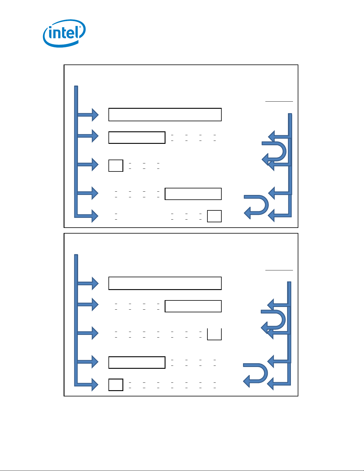
01234567
01234567
012345 6 7
012345 6 7
012 3 4567
012 3 4567
7 6 5 4 3210
0 1 2 3 4567
7 65432 1 0
0 12345 6 7
LP
76543210
01234567
7 6 5 4 3210
0 1 2 3 4567
7 6 5 4 3 2 1 0
0 1 2 3 4 5 6 7
012345 6 7
012345 6 7
012 3 4 5 6 7
012 3 4 5 6 7
defectandphysicallanes0‐3arevalid)
Case1:alllanesvalid
physicalLanes1‐3isdefectandatleast1ofphysicalLanes4‐7isdefect)
defectandphysicallanes4‐7arevalid)
Degradation:
Degradation:
Case1:alllanesvalid
physicalLanes4‐6isdefectandatleast1ofphysicalLanes0‐3isdefect)
Intel® Ethernet Controller X550 Datasheet—Interconnects
InitialConfiguration
LP 01234567
NIC 01234567
LP
NIC
Case2:atleast1ofphysicalLanes4‐7isdefect
LP
NIC
Case3:(Atleast1ofphysicalLanes1‐3isdefectandLPdoesn’tinitiatelanereversal)or (Atleast1of
LP
NIC
Case4:(Atleast1ofphysicalLanes 1‐3isdefectandLPinitiateslanereversal)or(Physicallane0is
LP
NIC
Case5:Physicallane0isdefectandatleastoneofphysicallanes4‐6aredefect
LP
NIC
InitialConfiguration
LP 76543210
NIC 01234567
NIC
Case2:atleastoneofphysicalLanes0‐3isdefect
LP
NIC
Case3:(Atleast1ofphysicalLanes4‐6isdefectandLPdoesn’tinitiatelanereversal)or (Atleast1of
LP
NIC
Case4:(Atleast1ofphysicalLanes 4‐6isdefectandLPinitiateslanereversal)or(Physicallane7is
LP
NIC
Case5:Physicallane7isdefectandatleastoneofphysicallanes1‐3aredefect
LP
NIC
Figure 3-2. Link Width Configurations for a x8 Port
62 333369-004
Page 63
Interconnects—Intel
0123
0123
012 3
012 3
3 2 1 0
0 1 2 3
3210
0123
3 2 1 0
0 1 2 3
012 3
012 3
Degradation:
Case2:atleast1ofphysicalLanes1‐3isdefect
Case3:Physicallane0isdefect
Case1:alllanesvalid
Degradation:
Case2:atleastoneofphysicalLanes0‐2isdefect
Case3:Physicallane3isdefect
Case1:alllanesvalid
NIC 0123
®
Ethernet Controller X550 Datasheet
InitialConfiguration
LP 0123
LP
NIC
LP
NIC
LP
NIC
InitialConfiguration
LP 3210
Figure 3-3. Link Width Configurations for a x4 Port
NIC 0123
LP
NIC
LP
NIC
LP
NIC
333369-004 63
Page 64

Intel® Ethernet Controller X550 Datasheet—Interconnects
0
0
Case1:alllanesvalid
InitialConfiguration
LP 0
NIC 0
LP
NIC
Figure 3-4. Link Width Configurations for a x1 Port
3.1.4.4 Receiver Framing Requirements
This section applies to Gen3 operation only and lists the optional capabilities defined in Section
4.2.2.3.3 (Receiver Framing Requirements) of the PCIe base specification.
The device implements the optional Gen3 receiver framing error checks other than:
• TLP Token length=0
• Mixed order sets across lanes
3.1.5 Error Events and Error Reporting
3.1.5.1 General Description
PCIe defines three error reporting paradigms: the baseline capability, the Advanced Error Reporting
(AER) capability, and a proprietary mechanism. The baseline error reporting capabilities are required of
all PCIe devices and define the minimum error reporting requirements. The AER capability is defined for
more robust error reporting and is implemented with a specific PCIe capability structure. Both
mechanisms are supported by the X550. The proprietary error reporting mechanism used for error
better handled by the software device driver using internal CSRs is described in Section 3.1.5.8.
The SERR# Enable and the Parity Error bits from the Legacy Command register also take part in the
error reporting and logging mechanism.
In a multi-function device, PCIe errors that are not related to any specific function within the device are
logged in the corresponding status and logging registers of all functions in that device. Figure 3-5
shows, in detail, the flow of error reporting in the X550.
64 333369-004
Page 65

Interconnects—Intel
Device Status ::
Correctable Error Detected
Device Status ::
Non-Fatal Error Detected
Device Status ::
Fatal Error Detected
Device Status ::
Unsupported Request Detected
Status ::
Signaled Target Abort
Status ::
Received Target Abort
Status ::
Received Master Abort
Status ::
Detected Parity Error
Root Error Status
Correctable Error Status
Correctable Error Mask
Uncorrectable Error Status
Uncorrectable Error Mask
Uncorrectable Error Severity
Status Reporting - Not Gated
Error Sources
(Associated with Port)
Device Control ::
Correctable Error Reporting Enable
Device Control ::
Unsupported Request Reporting Enable
Device Control ::
Non-Fatal Error Reporting Enable
Device Control ::
Fatal Error Reporting Enable
Report Error Command ::
Correctable Error Reporting Enable
Report Error Command ::
Non-Fatal Error Reporting Enable
Report Error Command ::
Fatal Error Reporting Enable
Interrupt
Command::
Parity Error Response
Bridge Control::
SERR Enable
Error Message
Processing
Rcv
Msg
Secondary Side Error Sources
System
Error
Root Control::
System Error on Correctable Error Enable
Root Control::
System Error on Non-Fatal Error Enable
Root Control::
System Error on Fatal Error Enable
Status::
Master Data Parity Error
Status::
Signaled System Error
Secondary Status::
Detected Parity Error
Secondary Status::
Signaled Master Abort
Secondary Status::
Received Target Abort
Secondary Status::
Received Target Abort
Bridge Control::
Parity Error Response Enable
Secondary Status::
Master Data Parity
Error
Secondary Status::
Received System Error
Either Implementation
Acceptable – the unqualified
version is more like PCI P2P
bridge spec
Command::
SERR# Enable
®
Ethernet Controller X550 Datasheet
Figure 3-5. Error Reporting Mechanism
333369-004 65
Page 66

Intel® Ethernet Controller X550 Datasheet—Interconnects
3.1.5.2 Error Events
Tab l e 3 -6 lists the error events identified by the X550 and the response in terms of logging, reporting,
and actions taken. Refer to the PCIe specification for the effect on the PCI Status register.
Table 3-6. Response and Reporting of PCIe Error Events
Error Name Error Events Default Severity Action
Physical Layer Errors
Receiver Error • 8b/10b decode errors.
• Packet Framing Error.
Data Link Errors
Bad TLP • Bad CRC.
•Illegal EDB.
• Wrong sequence number.
Bad DLLP • Bad CRC. Correctable
Replay Timer
Timeout
REPLAY NUM
Rollover
Data Link Layer
Protocol Error
TLP Errors
Poisoned TLP
Received
ECRC Check failed • Failed ECRC check. Uncorrectable
Unsupported
Request (UR)
Completion Timeout • Completion timeout timer
• REPLAY_TIMER expiration. Correctable
• REPLAY NUM rollover. Correctable
• Violations of flow control
initialization protocol.
• TLP with error forwarding. Uncorrectable
•Receipt of TLP with
unsupported request type.
• Receipt of an unsupported
vendor defined type 0
message.
• Invalid message code.
• Wrong function number.
• Received TLP outside BAR
address range.
• Receipt of a Request TLP
during D3hot, other than
Configuration and Message
requests.
expired.
Correctable
Send ERR_CORR
Correctable
Send ERR_CORR
Send ERR_CORR
Send ERR_CORR
Send ERR_CORR
Uncorrectable
Send ERR_FATAL
ERR_NONFATAL
Log Header
ERR_NONFATAL
Log Header
Uncorrectable
ERR_NONFATAL
Log header
Uncorrectable
ERR_NONFATAL
TLP to initiate NAK, drop data.
DLLP to drop.
TLP to initiate NAK, drop data.
DLLP todrop.
Follow LL rules.
Follow LL rules.
If completion TLP:
Error is non-fatal (default case):
• Send error message if advisory.
• Retry the request once and send
advisory error message on each failure.
• If fails, send uncorrectable error
message.
Error is defined as fatal:
• Send uncorrectable error message.
Error is non-fatal (default case):
• Send error message if advisory.
Error is defined as fatal:
• Send uncorrectable error message.
Send completion with UR.
Error is non-fatal (default case):
• Send error message if advisory.
Error is defined as fatal:
• Send uncorrectable error message.
66 333369-004
Page 67

Interconnects—Intel
®
Ethernet Controller X550 Datasheet
Table 3-6. Response and Reporting of PCIe Error Events (Continued)
Error Name Error Events Default Severity Action
Completer Abort • Received target access with
Unexpected
Completion
Receiver Overflow • Received TLP beyond
Flow Control
Protocol Error
Malformed TLP (MP) • Data payload exceed
Completion with
Unsuccessful
Completion Status
illegal data size per
Section 3.1.2.1.1.
• Received completion without a
request for it (Tag, ID, etc.).
allocated credits.
• Minimum initial flow control
advertisements.
• Flow control update for infinite
credit advertisement.
Max_Payload_Size.
• Received TLP data size does
not match length field.
• TD field value does not
correspond with the observed
size.
• PM messages that do not use
TC0.
• Usage of unsupported VC.
• Target request crosses a 4KB
boundary.
Uncorrectable.
ERR_NONFATAL
Log header
Uncorrectable
ERR_NONFATAL
Log Header
Uncorrectable
ERR_FATAL
Uncorrectable.
ERR_FATAL
Uncorrectable
ERR_FATAL
Log Header
No Action (already done
by originator of
completion)
Send completion with CA.
Discard TLP.
Receiver behavior is undefined.
Receiver behavior is undefined.
Drop the packet, free FC credits.
Free FC credits.
3.1.5.3 Completion Timeout Mechanism
The X550 supports completion timeout as defined in the PCIe specification.
The X550 controls the following aspects of completion timeout:
• Disabling or enabling completion timeout.
—The PCIe Completion Timeout Disable Supported bit in the Device Capabilities 2 Register
(Section 9.2.3.6.10) is hardwired to 1b to indicate that disabling completion timeout is
supported
—The PCIe Completion Timeout Disable bit in Device Control 2 Register controls whether
completion timeout is enabled
• A programmable range of timeout values.
— The X550 supports all four ranges as programmed in the Completion Timeout Ranges
Supported field of the Device Capabilities 2 Register. The actual completion timeout value is
written in the Completion Timeout Value field of Device Control 2 Register (Section 9.2.3.6.10)
The following sequence takes place when completion timeout is detected:
• The appropriate message is sent on PCIe as described in Ta b le 3-6 .
• The affected queue or client takes action based on the nature of the original request.
• An interrupt is issued to the respective PF.
333369-004 67
Page 68

Intel® Ethernet Controller X550 Datasheet—Interconnects
3.1.5.4 Error Forwarding (TLP Poisoning)
If a TLP is received with an error-forwarding trailer, the packet is dropped and is not delivered to its
destination. The X550 then reacts as listed in Tabl e 3- 6.
The following sequence takes place when a poisoned TLP is received:
• The appropriate message is sent on PCIe as described in Ta b le 3-6 .
• An interrupt is issued.
• If the TLP is a completion, a completion timeout follows at some later time. Processing continues as
described in Section 3.1.5.3.
System logic is expected to trigger a system-level interrupt to signal the operating system of the
problem. Operating systems can then stop the process associated with the transaction, re-allocate
memory to a different area instead of the faulty area, etc.
3.1.5.5 Completion with Unsuccessful Completion Status
A completion arriving with unsuccessful completion status (either UR or CA) is dropped and not
delivered to its destination. A completion timeout follows at some later time. Processing continues as
described in Section 3.1.5.3.
3.1.5.6 Error Pollution
Error pollution can occur if error conditions for a given transaction are not isolated to the error's first
occurrence. If the PHY detects and reports a receiver error, to avoid having this error propagate and
cause subsequent errors at the upper layers, the same packet is not signaled at the data link or
transaction layers. Similarly, when the data link layer detects an error, subsequent errors that occur for
the same packet are not signaled at the transaction layer.
3.1.5.7 Blocking on Upper Address
The PCI_UPADD register blocks master accesses from being sent out on PCIe if the TLP address
exceeds some upper limit. Bits [31:1] correspond to bits [63:33] in the PCIe address space,
respectively.
When a bit is set in GLPCI_UPADD[31:1], any transaction in which the corresponding bit in its address
is set, is blocked and not sent over PCIe. If all register bits are cleared, there is no effect (in other
words, no TLPs are blocked by this mechanism).
The PCI_UPADD register is loaded from NVM with a value allowing all addresses to pass. The software
device driver should override this value with a system dependent value.
Processing a blocked transaction:
• Write transaction
— The transaction is dropped.
— Set the “Exceeded upper address limit (write requests)” event in the PCIe errors register (see
Section 3.1.5.8).
— An interrupt is issued as described in Section 3.1.5.8.
68 333369-004
Page 69

Interconnects—Intel
®
Ethernet Controller X550 Datasheet
• Read transaction
— The transaction is dropped.
— Set the “Exceeded upper address limit (read requests)” event in the PCIe errors register (see
Section 3.1.5.8).
— The originating internal client is notified.
— The affected queue or client takes action based on the nature of the original request. An
interrupt is issued to the respective PF.
3.1.5.8 Proprietary Error Reporting
The PCIe specification defines how to report errors to system software. There are, however, error
events that the device driver should be aware of or that the device driver is in better position to handle
and recover from. This section describes the mechanism to report PCIe related errors to device drivers.
Several CSRs are dedicated to this functionality, with a separate bit allocated per error type (see
Tab l e 3 -7):
• The “PCIe Errors Reported” register (PCI_PCIERR - RO) indicates which errors are reported using
this mechanism. It is shared by all PFs. It is loaded from NVM. All non-reserved errors are enabled.
• The “PCIe Interrupt Cause” register (PCI_ICAUSE - RW1C) indicates pending errors for errors set in
the PCIe Errors Reported register. It is dedicated per PF.
• The “PCIe Interrupt Enable” register (PCI_IENA - RW) determines if an interrupt should be issued to
the respective PCI function on an error event. It is dedicated per PF.
Reporting an error to the PF driver involves the following steps:
• The device checks if the respective bit is set in the PCIe Errors Reported register. If cleared, done.
Else, continue
• The respective bit is set in the “PCIe Interrupt Cause” register
• If the respective bit is set in the “PCIe Interrupt Enable” register, an interrupt is issued to the PCI
function. The PCI_EXCEPTION cause is used (see the EICR register - Section 8.2.2.6.1).
Table 3-7. PCIe Errors Reported to Device Software
Error Event Index Description and Comments Function Association
Exceeded upper address
limit (read requests)
Exceeded upper address
limit (write requests)
Reserved 02 Reserved entries N/A
Poisoned TLP received 03 See Section 3.1.5.4 Sent to PF
Reserved 04-05 Reserved entries N/A
ECRC error detected 06 ECRC check failed on a received TLP. See
Unsupported Request Request Type
Unsupported Request Vendor Message
333369-004 69
00 See Section 3.1.5.7 Sent to PF
01 See Section 3.1.5.7 Sent to PF
Section 3.1.5.7
07 Request causes an Unsupported Request due to
receipt of TLP with unsupported Request Type
08 Request causes an Unsupported Request due to
receipt of an Unsupported Vendor Defined Type 0
Message
Sent to all PFs
Sent to PF
Sent to PF unless r[2:0] =
Broadcast from Root Complex, in
which case sent to all PFs
Page 70

Intel® Ethernet Controller X550 Datasheet—Interconnects
Table 3-7. PCIe Errors Reported to Device Software (Continued)
Error Event Index Description and Comments Function Association
Unsupported Request Message Code
Unsupported Request Function Number
Unsupported Request Address Range
Unsupported Request D3hot
Completer abort - target
size
Reserved 14 - 31 Reserved entries N/A
09 Request causes an Unsupported Request due to
receipt of an invalid Message Code
10 Request causes an Unsupported Request due to
receipt of a not-supported Function Number
11 Request causes an Unsupported Request due to
receipt of a not-supported Address Range
12 Request causes an Unsupported Request due to
receipt of a Request TLP during D3hot, other than
Configuration and Message requests
13 Received Target Access with illegal data size per
Section 3.1.2.1.1 (CA)
Sent to PF
Sent to all PFs
Sent to PF
Sent to PF
Sent to PF
3.1.6 Performance and Statistics Counters
The X550 incorporates counters to track the behavior and performance of the PCIe interconnect. The
X550 implements several types of counters:
• Transaction layer event counters — Section 3.1.6.1
• Link and Physical layer event counters — Section 3.1.6.2
• Bandwidth counters — Section 3.1.6.3
• Latency counters — Section 3.1.6.4
General characteristics of the counters:
• Software can reset, stop, or start the counters.
• The counters are shared by all PCI functions (“Service” mode of sharing).
Part of the registers that manage the operation of the performance counters are accessed via the
PCI_LCBADD and PCI_LCBDATA register pair.
Reading a register via the PCI_LCBADD/PCI_LCBDATA pair is done as follows:
• Write the following values into the PCI_LCBADD register.
— ADDRESS — The 18-bit register address. See below for the specific address per each register.
— BLOCK_ID — Defines the sub-unit where the register resides. Use the value 0x7F to access
registers mentioned in this section.
— LOCK — Use if need to gain access in case of multiple agents accessing the PCI_LCBADD/
PCI_LCBDATA registers.
• Read the PCI_LCBDATA register.
Note: Although PCI_LCBDATA is a 32-bit register, the registers that maintain the actual count
are read as atomic 64-bit reads. The PCI_LCBADD contains the address of the low DW,
and reading PCI_LCBDATA returns a 64-bit value.
70 333369-004
Page 71

Interconnects—Intel
®
Ethernet Controller X550 Datasheet
Writing a register via the PCI_LCBADD/PCI_LCBDATA pair is done as follows:
• Write the following values into the PCI_LCBADD register.
— ADDRESS — The 18-bit register address. See below for the specific address per each register.
— BLOCK_ID — Defines the sub-unit where the register resides. For actual values, consult the text
below.
— LOCK — Use if need to gain access in case of multiple agents accessing the PCI_LCBADD/
PCI_LCBDATA registers.
• Write to the PCI_LCBDATA register.
3.1.6.1 Event Counters - Transaction Layer
Counters operate in one of the following modes:
• Count Mode — The counter increments when the respective event occurred
• Leaky Bucket Mode — The counter increments only when the rate of events exceeded a certain
value. See Section 3.1.6.1.2 for more details.
The list of events supported by the X550 are listed in Tabl e 3 -8 .
Table 3-8. PCIe Statistic Events Encoding
Events
Cycles 0x00 Increment on each PCIe clock tick
Bad Request TLPs 0x10 Number of bad TLPs arriving to the transaction layer.These include:
Bad Completions 0x11 Number of bad Completions received. These include:
Completion Timeout 0x12 Number of completion timeout events
Poisoned TLP 0x13 Number of TLPs received with poisoned data
ECRC Check 0x14 Number of TLPs that foil ECRC check
Retry Buffer Timeout 0x31 Number of replay events that happen due to timeout (does not count replay
Retry Buffer Replay Roll-Over 0x32 Increment when a replay is initiated for more than 3 times
Receive Error 0x50 Increment when one of the following occurs:
Surprise Link Down 0x51 Increment when link is unpredictably down (Not because of reset or DFT)
Event
Mapping
(Hex)
Description
Transaction Layer Events
• Request caused UR
• Request caused CA
• Malformed TLP
• Unexpected Completion
•UR status
•CA status
Link Layer Events
initiated due to NACK)
Physical Layer Events
1. Decoder error occurred during training in the PHY. It is reported only when
training ends.
2. Decoder error occurred during link-up or till the end of the current packet (in
case the link failed). This error is masked when entering/exiting EI.
333369-004 71
Page 72

Intel® Ethernet Controller X550 Datasheet—Interconnects
3.1.6.1.1 Count Mode
The following CSR fields control operation of the Count mode:
• Four 32-bit counters PCI_GSCN_0_3 track events and increment on each occurrence of an event.
— The four 32-bit counters can also operate in a two 64-bit mode to count long intervals or large
payloads.
• Registers PCI_GSCN_0_3[0] and PCI_GSCN_0_3[1] form the first 64-bit counter. Registers
PCI_GSCN_0_3[2] and PCI_GSCN_0_3[3] form the second 64-bit counter.
• The PCI_GSCL_1.GIO_64_BIT_EN selects between 32-bit and 64-bit modes.
• The PCI_GSCL_1.GIO_COUNT_EN_[3:0] bits enable each of the 4 counters.
— The enable bits for the two 64-bit counters are PCI_GSCL_1.GIO_COUNT_ EN_0 and
PCI_GSCL_1.GIO_COUNT_ EN_2, respectively.
• The PCI_GSCL_1.GIO_COUNT_START bit starts event counting of enabled counters.
• The PCI_GSCL_1.GIO_COUNT_STOP bit stops event counting of running counters.
• The PCI_GSCL_1.GIO_COUNT_RESET bit resets the event counters.
• The PCI_GSCL_2 associates an event with each of the 4 counters.
—In 64-bit mode, the GIO_EVENT_NUM_[2,0] fields are used.
3.1.6.1.2 Leaky Bucket Mode
Each of the counters can be configured independently to operate in a leaky bucket mode. When in leaky
bucket mode, the following functionality is provided:
• One of four 16-bit Leaky Bucket Counters (LBC) is enabled via the LBC_ENABLE_[3:0] bits in the
PCIe Statistic Control register #1.
• The LBC is controlled by the GIO_COUNT_START, GIO_COUNT_STOP, GIO_COUNT_RESET bits in
the PCIe Statistic Control register #1.
• The LBC increments every time the respective event occurs.
• The LBC is decremented every T s as defined in the LBC_TIMER_N field in the PCIe Statistic
Control registers #5...#8 (PCI_GSCL_5_8).
• When an event occurs and the value of the LBC meets or exceeds the threshold defined in the
LBC_THRESHOLD_N field in the PCIe Statistic Control registers #5...#8 (PCI_GSCL_5_8), the
respective statistics counter increments, and the LBC counter is cleared to zero.
3.1.6.2 Event Counters - Link and Physical Layers
This section describes the performance events for the Link and Physical layers and how to manage the
counters associated with these events.
Note: Before using LCB performance counters, the clock gating should be disabled by setting the
PCIE_CLKGATE_DIS field in the PCI_GLBL_CNF register.
The registers responsible for the Link and Physical layers counters are accessed via the PCI_LCBADD
and PCI_LCBDATA register pair.
Two events can be counted concurrently. The event counters include two sets of registers, each
managing one event counter. Such pairs are documents as <register_name>[1:0].
72 333369-004
Page 73

Interconnects—Intel
®
Ethernet Controller X550 Datasheet
The following procedures manage the operation of the event counters (when writing to part of the
register, make sure other fields are written with their existing values):
• Resetting the counters configuration:
— Set the XPPERFCON.GRST bit.
— Clear the XPPERFCON.GRST bit (otherwise the logic stays in reset).
• Setting an event:
— Write 0x0...0 to the XPPMCL[1:0] registers
— Set the XPPMR[1:0].CENS field to 0x1
— Set the XPPMR[1:0].CNTMD field to 0x1
— Set the XPPMER[1:0].XPRSCA field to 0x1
— Set the event according to Tab le 3-9 .
• Starting a count:
— Set the XPPERFCON.GCE bit.
• Stopping a count:
— Clear the XPPERFCON.GCE bit.
• Reading the count (note: reading the counter clears their values):
— Read the respective XPPMDH[1:0] and XPPMDL[1:0] register pair in a single 64-bit aligned
access.
Tab l e 3 -9 defines the Link and Physical Layer events.
Table 3-9. Link and Physical Layer Performance Events
Event Description Register Field
Uncorrectable Errors Counts the total number of Uncorrectable Errors. XPPMER[1:0].CNTUCERR
Correctable Errors Counts the total number of Correctable Errors. XPPMER[1:0].CNTCERR
Tx L0s state utilization Counts the number of entries to L0s on the Tx lanes. XPPMER[1:0].TXL0SU
Rx L0s state utilization Counts the number of entries to L0s on the Rx lanes. XPPMER[1:0].RXL0SU
Link Utilization Counts clocks that a port is receiving data.
If one counter counts receiver errors and another counter counts
Link Utilization, a bit error rate can be calculated.
Recovery State Utilization Counts the number of entries to Recovery state. XPPMER[1:0].RECOVERY
ASPM L1 state utilization Counts the number of entries to ASPM L1 state (i.e. initiated by
SW L1 state utilization Counts the number of entries to L1 state initiated by software. XPPMER[1:0].SWL1
Tx and Rx L0s utilization Counts number of events where both Tx and Rx are in L0s state. XPPMER[1:0].RXL0STXL0SU
NAK DLLP received Counts number of received NAK DLLPs. XPPMER[1:0].NAKDLLP
the device).
XPPMER[1:0].LNKUTIL
XPPMER[1:0].L1
333369-004 73
Page 74

Intel® Ethernet Controller X550 Datasheet—Interconnects
3.1.6.3 Bandwidth Counters
The bandwidth counters measure total payload bytes transferred over the PCIe link. Counting is
provided per each traffic type (posted, non-posted, completions) per direction (upstream,
downstream).
The mechanisms described above hold for the bandwidth counters with the following differences:
• Setting an event:
— Set the XPPMR[1:0].CENS field to 0x1.
— Set the XPPMR[1:0].EGS field to 0x2.
— Set the XPPMR[1:0].FCCSEL field to the desired traffic type (posted, non-posted, completions,
or all).
— Set the XPPPMER[1:0].TXRXSEL field to desired values.
— Set the XPPPMER[1:0].XPRSCA field to 0x1.
— Set the XPPERFCON.GCE field to 0x1.
Registers fields used exclusively by the bandwidth counters:
• XPPMR[1:0].FCCSEL — Selects the desired traffic type (posted, non-posted, completions, or all).
•XPPMER[1:0].TXRXSEL — Selects between monitoring downstream traffic, upstream traffic, or
both.
3.1.6.3.1 Register Map
The register fields that control the Link and Physical Layer events are as follows:
Table 3-10. XP PM Compare Low Bits Register (XPPMCL[1:0]) (0x3288, 0x328C)
Field Bit(s) Init. Description
CMPL 31:0 0xFF...F PM Compare Low Value
Low order bits [31:0] for PM compare register[1:0].
Table 3-11. XP PM Data Low Bits Register (XPPMDL[1:0]) (0x32E8, 0x32F0)
Field Bit(s) Init. Description
CNTL 31:0 0x00...00 PM Data Counter Low Value
Note: XPPMDL must be read together with the respective XPPMDH register as a single 64-bit aligned read. The registers are
simultaneously cleared on read.
Table 3-12. XP PM Data High Bits Register (XPPMDH[1:0]) (0x32EC, 0x32F4)
Field Bit(s) Init. Description
CNTH 3:0 0x0 PM Data Counter High Value
RSVD 31:4 0x0...0 Reserved.
Note: XPPMDH must be read together with the respective XPPMDL register as a single 64-bit aligned read. The registers are
simultaneously cleared on read.
Low order bits [31:0] for PM data counter[1:0].
High order bits [35:32] for PM data counter[1:0].
74 333369-004
Page 75

Interconnects—Intel
®
Ethernet Controller X550 Datasheet
Table 3-13. XP PM Response Control Register (XPPMR[1:0]) (0x3294, 0x3298)
Field Bit(s) Init. Description
RSVD 10:0 0x0 Reserved.
CENS 13:11 00b Counter Enable Source
CNTMD 15:14 00b Count Mode
EGS 20:19 00b Event Group Selection
RSVD 31:21 0x0 Reserved.
Table 3-14. XP PM Resource Events Register (XPPMER[1:0]) (0x32AC, 0x32B0)
Field Bit(s) Init. Description
TXRXSEL 1:0 00b Tx/Rx Select
FCCSEL 4:2 000b Flow Control Class Select
RSVD 12:5 0x0 Reserved.
LNKUTIL 16:13 0x0 Link Utilization
XPRSCA 20:17 0x0 XP Resource Assignment
RXL0SU 21 0b Rx L0s State Utilization Event
TXL0SU 22 0b Tx L0s State Utilization Event
CNTCERR 23 0b Count Correctable Errors
CNTUCERR 24 0b Count Uncorrectable Errors
RECOVERY 25 0b Recovery State Utilization
L1 26 0b ASPM L1 State Utilization
SWL1 27 0b SW L1 State Utilization
This field selects the traffic direction to monitor:
1xb = Transmit
x1b = Receive (from PCIe bus)
11b = Either Transmit or Receive direction.
This field selects which flow class for resource event
xx1b = Posted
x1xb = Non-Posted
1xxb = Completion
Note: Setting to 111b counts posted, non-posted, and completion traffic combined.
Set to 0x1 to enable.
0001b = Set
All other values are reserved.
0b = Disabled
1b = Enabled
0b = Disabled
1b = Enabled
0b = Disabled
1b = Enabled
0b = Disabled
1b = Enabled
0b = Disabled
1b = Enabled
0b = Disabled
1b = Enabled
0b = Disabled
1b = Enabled
333369-004 75
Page 76

Intel® Ethernet Controller X550 Datasheet—Interconnects
Table 3-14. XP PM Resource Events Register (XPPMER[1:0]) (0x32AC, 0x32B0) (Continued)
Field Bit(s) Init. Description
RXL0STXL0SU 28 0b Tx and Rx L0s Utilization
0b = Disabled
1b = Enabled
NAKDLLP 29 0b NAK DLLP Received
0b = Disabled
1b = Enabled
RSVD 31:30 0x0 Reserved.
Table 3-15. Performance Monitor Local Control Register (XPPERFCON) (0x32C4)
Field Bit(s) Init. Description
GRST 0 0b Global Reset
GCE 1 0b Global Count Enable
RSVD 31:2 0x0 Reserved.
3.1.6.4 Latency Counter
The latency counter measures the min, max, or average read latency.
Note: Completion Timeout events are ignored when the latency counter is enabled.
The latency counters are managed via a set of register fields described below (see also Tabl e 3-1 6,
Tab l e 3 -17 , and Tab le 3-1 8). Each of the following sources of traffic has its separate set of registers and
counters:
0x0 — Rx LAN descriptor fetch
0x1 — Tx LAN descriptor fetch
0x4 — Internal cache load
0x5 — Internal management engine read
0x6 — Tx LAN packet fetch
The registers are accessed via the PCI_LCBADD and PCI_LCBDATA registers.
The register fields that control the latency counter operation are:
Table 3-16. NPQ Control Register - NPQC (0x00000)
Field Bit(s) Init. Description
Reserved 3:0 0x4 Reserved.
PERFMNTRAVG 7:4 0x1 Performance Monitor Average Rate
PERFMNTREN 8 0b Performance Monitor Enable
This field sets the averaging rate for all latency average monitors. See definition of
NPQRTDLY1.ARTDLY (Tabl e 3 -1 7).
This field divided by 16 is the weight W in an exponential moving average. The possible
values are 1, 2, 4 or 8, which correspond to averaging rates of 0.0625, 0.125, 0.25 or
0.5, respectively.
This bit should set to enable latency counters.
Clearing this bit clears the latency counters.
76 333369-004
Page 77

Interconnects—Intel
®
Ethernet Controller X550 Datasheet
Table 3-16. NPQ Control Register - NPQC (0x00000) (Continued)
Field Bit(s) Init. Description
RTMNTREN 9 0b Latency Counting Enable
This bit should set to enable latency counters. When set, completion timeout events are
ignored.
Reserved 31:10 0x0 Reserved.
Table 3-17. NPQ Round-Trip Delay 1 Register - NPQRTDLY1 (0x00030; RO)
Field Bit(s) Init. Description
ARTDLY 15:0 0x0 Average Read Requests Round-trip Delay
Reserved 31:16 0x0 Reserved.
Captures the average read latency experienced since the last counter reset.
Latency is measured from time the read request starts until the time the completion starts
to arrive. Average is calculated as exponential moving average. That is, the new average
M(n) at sample n equals:
M(n) = (W/16) * new_sample + (16-W)/16*M(n-1)
where W is defined in the NPQC.PERFMNTRAVG field.
Table 3-18. NPQ Round-Trip Delay 2 Register - NPQRTDLY2 (0x00034; RO)
Field Bit(s) Init. Description
MINRTDLY 15:0 0x0 Minimal Read Requests Round-Trip Delay
Captures the minimal read latency experienced since the last counter reset.
Latency is measured from time the read request starts until the time the completion starts
to arrive.
MAXRTDLY 31:16 0x0 Maximal Read Requests Round-Trip Delay
Captures the maximal read latency experienced since the last counter reset.
Latency is measured from time the read request starts until the time the completion starts
to arrive.
Latencies are measured in cycle counts, where a cycle duration is per Tab le 3- 19 .
Table 3-19. Resolution of the Latency Counters
PCIe Operation Speed
Gen1 (2.5G) 0b x 8
Gen2 (5.0G) 0b x 4
Gen3 (8.0G) 0b x 2
Gen1 (2.5G) 1b 8 lanes 16
Gen2 (5.0G) 1b 8 lanes 8
Gen1 (2.5G) 1b 1 or 4 lanes 32
Gen2 (5.0G) 1b 1 or 4 lanes 16
Gen3 (8.0G) 1b 1 or 4 lanes 8
Setting of the
PCI_CLKCTL.PCI_CLK_DYN
Bit
PCIe Operational Link
Width
Cycle Duration (ns)
333369-004 77
Page 78

Intel® Ethernet Controller X550 Datasheet—Interconnects
3.2 Management Interfaces
The X550 contains three possible interfaces to an external BMC.
•SMBus
• NC-SI (over RMII)
• MCTP (over PCIe or SMBus)
3.2.1 SMBus
SMBus is an optional interface for pass-through and/or configuration traffic between an external BMC
and the X550. The SMBus channel behavior and the commands used to configure or read status from
the X550 are described in Section 11.5.
The X550 also enables reporting and controlling the device using the MCTP protocol over SMBus. The
MCTP interface is used by the BMC to control the NIC and for pass-through traffic. All network ports are
mapped to a single MCTP endpoint on SMBus. For information, refer to Section 11.5.
3.2.1.1 Channel Behavior
The SMBus specification defines a maximum frequency of 100 KHz. However, when acting as a slave,
the X550 can receive transaction with a clock running at up to 1 MHz. When acting as a master, it can
toggle the clock at 100 KHz, 400 KHz or 1 MHz. The speed used is set by the SMBus Connection Speed
field in the SMBus Notification Timeout and Flags NVM word (Section 6.5.4.3).
3.3 Network Controller — Sideband Interface (NC-SI)
The NC-SI interface in the X550 is a connection to an external MC. It operates as a single interface with
an external BMC, where all traffic between the X550 and the BMC flows through the interface.
The X550 NC-SI interface meets the NC-SI version 1.0.0 specification as a PHY-side device.
3.3.1 Electrical Characteristics
The X550 complies with the electrical characteristics defined in the NC-SI specification.
3.3.2 NC-SI Transactions
The NC-SI link supports both pass-through traffic between the BMC and the X550 LAN functions, as well
as configuration traffic between the BMC and the X550 internal units as defined in the NC-SI protocol.
Refer to Section 11.6.2 for information.
78 333369-004
Page 79

Interconnects—Intel
®
Ethernet Controller X550 Datasheet
3.3.3 MCTP (Over PCIe or SMBus)
The X550 supports MCTP protocol for management. MCTP runs over PCIe or SMBus. The X550
implements NC-SI over MCTP protocol for command and pass-through traffic. See Section 11.7 for
details.
3.4 Non-Volatile Memory (NVM)
3.4.1 General Overview
The X550 uses a Flash device to store product configuration information. The Flash is divided into three
general regions:
• Hardware Accessed — Loaded by the the X550 hardware after power-up, PCI reset de-assertion,
D3 to D0 transition, or software reset. Different hardware sections in the Flash are loaded at
different events. For more details on power-up and reset sequences, see Section 4.1 and
Section 4.2.
• Firmware Area — Includes firmware code and structures used by the firmware for management
configuration in its different modes.
• Software Accessed — This region is used by software entities such as LAN drivers, option ROM
software and tools, PCIe bus drivers, VPD software, etc.
3.4.1.1 NVM Protection
The NVM protection method implemented in the X550 relies on an “authenticate on update” concept. It
means that the protected modules are not authenticated after initialization, but prior to committing a
module update operation only. NVM protection is guaranteed by an inductive authentication chain, that
assumes an initial secured NVM image and requires that any NVM update must be secure as well. This
method mandates the following limitations and restricting working assumptions:
1. An initial ‘good’ image is loaded into the flash at the manufacturing site which is assumed to be
safe.
— It assumes customers (OEM and end-user) know the source of the installed components, the
supply chain producing these components is not compromised during manufacturing, and that
the NIC/LOM is physically protected from modification after deployment.
— The possibility exists that unauthorized firmware may be loaded into the NVM via physical
modification post manufacturing, as well as through supply chain vulnerabilities. However,
firmware updates via programmatic (software) methods are enhanced to require authentication
prior to updating NVM settings. Furthermore, host software can independently detect whether
the firmware image has an invalid digital signature.
2. In a normal operating mode, NVM write accesses are controlled by the device (firmware) and
cannot be performed via the memory mapped accesses, EEWR register, or bit-banging. Memory
mapped NVM access remains available for NVM read accesses only. For simplicity and flexibility
reasons, NVM write accesses from the host can be initiated via host interface commands
(Section 11.8.3.3), VPD write interface, or via a BMC command, which are all handled by firmware.
Memory BAR writes, EEWR and FLA bit-banging accesses are blocked by hardware when the NVM is
protected.
333369-004 79
Page 80

Intel® Ethernet Controller X550 Datasheet—Interconnects
3. All the supported Flash parts share the same set of op-codes as described in Section 3.4.1.2. A
blank Flash programming mode is provided (besides the normal programming mode previously
mentioned in item 2), where the Flash can be programmed directly without firmware involvement
via the FLA bit-banging or Flash BAR interfaces. This mode is indicated by FLA.LOCKED = 0b.
3.4.1.2 Flash Device Requirements
The X550 supports Flash devices with a sector erase size of 4 KB and an address width of 24 bits (up to
4 MB). Note that many Flash vendors are using the term sector differently. This document uses the
term Flash sector for a logic section of 4 KB.
The X550 supports Flash devices that are either write-protected by default after power-up or not. The
X550 is responsible to remove the protection by sending the write-protection removal Op-Code to the
Flash after power up.
The following Op-Codes are supported by the X550 as they are common to all supported Flash devices:
1. Write Enable (0x06)
2. Read Status Register (0x05) - used by hardware internally.
3. Write Status Register (0x01). The written data is 0x00 to cancel the Flash default protection. Used
by hardware internally.
4. Read Data (0x03). Burst read is supported.
5. Byte Program (0x02). To program a data byte.
6. 4 KB Sector-Erase (0x20)
7. Chip-Erase (0xC7)
8. Read JEDEC ID (0x9F)
3.4.1.2.1 Flash Identification
The Flash connected to the X550 can be identified by its JEDEC ID that can be read using the Flash Info
host interface command (Section 11.8.3.3.9). This identification is available only if a valid Flash is
installed. If the Flash is empty or with an invalid signature, software can read the JEDEC ID by applying
an RDID command (opcode 0x9F) or a Read SFDP command (opcode 0x5A) via the bit-bang interface.
3.4.2 Shadow RAM
The first eight 4 KB sectors of the X550’s Flash are allocated to create two 16 KB sections (section 0 and
section 1), for the configuration content. At least one of these two sections must be valid at any given
time or else the X550 is set to hardware default. Following a Power On Reset (POR), the X550 copies
the valid section of the Flash device into an internal Shadow RAM. Any further read accesses of the
software or firmware to the lower 16 KB addresses of the NVM (not through flash BAR) are directed to
the internal Shadow RAM. Modifications made to the Shadow RAM content are copied by the X550 into
the other 16 KB section of the NVM, circularly flipping the valid section between sections 0 and 1 in the
NVM.
This mechanism provides the following advantages:
1. A way to protect the image-update procedure from power down events by establishing a doubleimage policy. See Section 3.4.8.1 for a description of the double-image policy. It relies on having
pointers to NVM modules stored in the NVM section mirrored in the internal Shadow RAM.
80 333369-004
Page 81
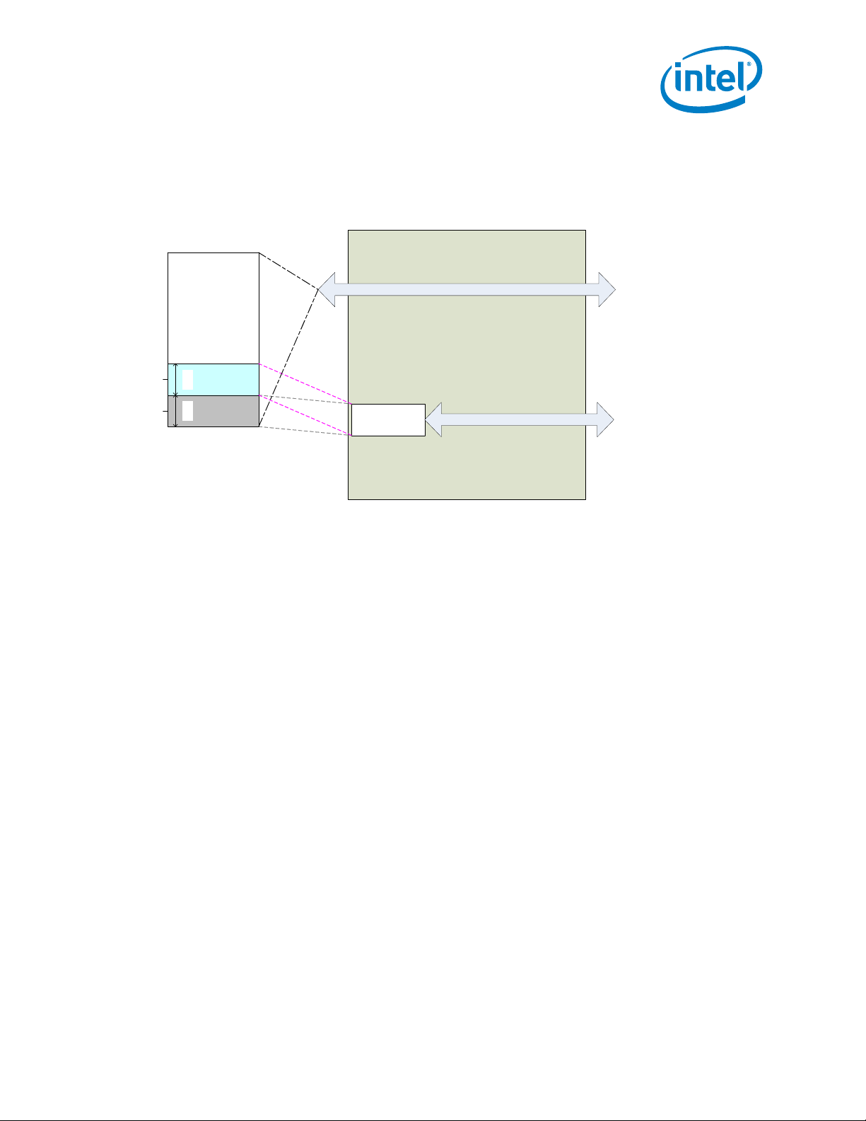
Interconnects—Intel
Section 0
Section 1
Shadow RAM
X550
Flash
EEPROM-
Mode Access
0x003FFF 0x000000
0x000000
0x003FFF
0x004000
0x007FFF
0x008000
0xFFFFFF
0x000000
0x003FFF
1:1
Physical Byte
address
Flash-Mode
Access
0xFFFFFF 0x000000
Logical
address
Internal RAM
address
16
KB
16
KB
®
Ethernet Controller X550 Datasheet
2. A way to ensure hardware auto-load during a PCIe reset event can be completed within PCIe timing
constraints (100 ms), even if the Flash is busy performing an erase operation initiated prior to that
reset event.
Figure 3-6 shows the Shadow RAM mapping and interface.
Figure 3-6. NVM Shadow RAM
3.4.2.1 Shadow RAM Update Flow
Following a write access by the software device driver to update the Shadow RAM, the data should be
updated in the Flash as well. The X550 updates the Flash from the Shadow RAM when software
explicitly requests to update the Flash using the Shadow RAM Dump host interface command
(Section 11.8.3.3.8). To reduce Flash update operations, software is expected to request a dump only
once its last Shadow RAM update access completes. The X550 then copies the content of the Shadow
RAM to the non valid configuration section and makes it the valid one.
3.4.3 NVM Clients and Interfaces
There are different software clients that can access the NVM: driver, tools, BIOS, VPD, etc.
Tab l e 3 -20 lists the different accesses to the NVM.
333369-004 81
Page 82

Intel® Ethernet Controller X550 Datasheet—Interconnects
Table 3-20. Clients and Access Types to the NVM
Client
Host
Software
Firmware
or
Software
NVM Access
Method
(Data Width)
Memory BAR
(parallel 32-bit)
FLA bit-banging
(serial 1-bit)
Host interface
Shadow RAM
Read/Write
command
Host interface
Flash read
command
Host interface
Flash write
command/Flash
block erase
command
VPD access
(parallel 32-bit)
FLMNG
Parallel
(Read: 32-bits
Write: 8-bits)
NVM
Access
Target
Flash 0x000000 -
Flash 0x000000 -
Shado
w RAM
Flash 0x000000 -
Flash 0x008000 -
Shado
w RAM
Flash 0x000000 -
Logical
Byte
Address
Range
0xFFFFFF
0xFFFFFF
0x000000 0x003FFF
0xFFFFFF
0xFFFFFF
0x000000 0x0003FF
0xFFFFFF
NVM Access Interface Protection and Enforcement
Memory mapped read/write via
BARs.
Software accesses to Flash by
toggling the SPI pins.
Access to Shadow RAM through
the Shadow RAM Read/Write
command
Software read from Flash via
Flash Read command.
Software write to sector/Flash
erase
VPD Address and Data
registers.
FLMNGCTL and FLMNGDATA
registers accesses to the FLASH
Write access is limited to a single byte,
and is allowed only if hardware
protection is disabled (FLA.LOCKED =
0).
FLA interface access is available only if
hardware protection is disabled
(FLA.LOCKED = 0).
Requires a valid firmware image.
Write protection is enforced by
firmware.
Requires a valid firmware image.
Requires a valid firmware image.
Writes to protected areas are dropped
when protection (enforced by firmware)
is enabled. Protected sector erase or a
complete Flash erase requests are
rejected when protection (enforced by
firmware) is enabled.
Write accesses are enabled to the R/W
area of the VPD
If the VPD structure is not valid, the
entire 1024 bytes area is RO.
Software access is available only when
protection is disabled.
3.4.3.1 Memory Mapped Host Interface
Using the legacy Flash transactions, the Flash is accessed by the X550 each time the host CPU performs
a read or a write operation to a memory location mapped to the Flash address space, or upon boot via
accesses in the space indicated by the Expansion ROM Base Address register. Accesses to the Flash are
based on a direct decode of CPU accesses to a memory window defined in either:
• Memory CSR + Flash Base Address Register (PCIe Control Register at offset 0x10).
• The Expansion ROM Base Address Register (PCIe Control Register at offset 0x30).
• The X550 is responsible to map accesses via the Expansion ROM BAR to the physical NVM. The
offset in the NVM of the Expansion ROM module is defined by the PCIe Expansion/Option ROM
Pointer (NVM word address 0x05). This pointer is loaded by the X550 from the NVM before enabling
any access to the Expansion ROM memory space.
The X550 controls accesses to the Flash when it decodes a valid access. Attempt to out of range read
access the PCIe Expansion/Option ROM module (according to NVM Size field in NVM Control Word 1)
would return a value of 0xDEADBEEF. Attempt to memory-mapped write accesses to the Flash when
protection is enabled or via expansion ROM BAR are ignored.
82 333369-004
Page 83

Interconnects—Intel
®
Ethernet Controller X550 Datasheet
3.4.4 Flash Access Contention
Flash accesses initiated through different LAN functions might occur concurrently. The X550 does not
synchronize between entities accessing the Flash, so a contention caused from one entity reading and
another modifying the same location is possible.
To avoid such contention between software LANs or between software and firmware accesses, these
entities are required to make use of the semaphore registers. Refer to Section 11.8.4. Any read or write
access to the NVM made by software/firmware must be preceded by acquiring ownership over the NVM.
This is also useful to avoid the time out of a PCIe transaction made to a memory mapped Flash address
while the Flash is busy performing a sector erase operation.
However, two software entities cannot use this semaphore mechanism: BIOS access through expansion
ROM and VPD software.
• Since VPD software accesses only the VPD module, which is located in the configuration section of
the NVM, VPD accesses are always performed against the Shadow RAM. Firmware must take NVM
ownership before dumping the VPD changes to the Flash. The Shadow RAM dump sequence is
described in Section 3.4.2.1.
• No contention can occur between the BIOS access through expansion ROM and other software
entities (including VPD) as it accesses the NVM while the operating system is down.
• Contentions between BIOS and firmware can however happen if a system reboot occurs while the
MC is accessing the NVM.
— If a system reboot is caused by a user pressing the standby button, it is required to route the
wake-up signal from the standby button to the MC and not to the chipset. The MC issues a
system reboot signal to the chipset only after the NVM write access completes. Firmware is
responsible to respond with a “busy” error code to MC NC-SI commands while other NVM writes
are in progress.
— If a system reboot is issued by a local user on the host, there is no technical way to prevent
NVM access contentions between the BIOS and the MC.
Caution: It is the user’s responsibility when remotely accessing the NVM via the MC, to make sure
another user is not currently initiating a local host reboot.
Notes: The PHY auto-load process from the Flash device is made up of short read bursts (32-bits)
that can be inserted by hardware in between other NVM clients’ accesses, at the lowest
priority. It is the user’s responsibility to avoid initiating a PHY auto-load while updating the
PHY NVM modules.
The MAC auto-load from the Flash device itself occurs after power-up only, before host or
firmware can attempt to access the Flash. The host must wait until PCIe reset is de-asserted
(after ~1 second, which is enough time for the MAC auto-load to complete), and firmware
starts its auto-load after the EEC.MNG_READY bit is asserted by hardware.
Other MAC auto-load events are performed from the internal Shadow RAM and do not
compete with memory mapped accesses to the Flash device. During such MAC auto-loads,
accesses from other clients via EEPROM-Mode registers are delayed until the auto-load
process completes.
Software and firmware should avoid holding Flash ownership (via the dedicated semaphore
bit) for more than 500 ms.
333369-004 83
Page 84

Intel® Ethernet Controller X550 Datasheet—Interconnects
3.4.4.1 Flash Deadlock Avoidance
The Flash is a shared resource between the following clients:
1. Hardware auto-load of Shadow RAM (at power up).
2. LAN port 0 and LAN port 1 software accesses.
3. Manageability/firmware accesses.
4. Software tools.
All clients can access the Flash using parallel access. Hardware implements the actual access to the
Flash. Hardware arbitrates between the different clients and schedules these accesses, avoiding
starvation of any client.
However, the software and firmware clients can access the Flash using bit-banging. In this case, there is
a request/grant mechanism that locks the Flash to the exclusive use of one client. If one client is stuck
without releasing the lock, the other clients can no longer access the Flash. To avoid this deadlock, the
X550 implements a time-out mechanism, which revokes the grant from a client that does not toggle the
Flash bit-bang interface (FLA.FL_SCK bit) for more than 2 seconds. If any client fails to release the
Flash interface, hardware clears its grant, enabling the other clients to use the interface.
The deadlock timeout mechanism is enabled by the Deadlock Timeout Enable bit in NVM Control Word 2
in the Flash.
3.4.5 Signature Field
The only way the X550 can tell if a Flash is present is by trying to read the Flash. The X550 first reads
the Control word at word address 0x0 and at word address 0x2000. It then checks the signature value
at bits 7 and 6 in both addresses.
If bit 7 is 0b and bit 6 is 1b in (at least) one of the two addresses, it considers the Flash to be present
and valid. It then reads the additional Flash words from that section and programs its internal registers
based on the values read. Otherwise, it ignores the values read from that location and does not read
additional words.
If the signature bits are valid at both addresses the X550 assumes that the first section is the valid one.
3.4.6 VPD Support
The Flash image can contain an area for VPD. This area is managed by the OEM vendor and does not
influence the behavior of hardware. Word 0x2F of the Flash image contains a pointer to the VPD area in
the Flash. A value of 0xFFFF means VPD is not supported and the PCI_CAPCTRL.VPD_EN bit should be
cleared in the PCI NVM section (Section 6.4.5), to prevent the VPD capability from appearing in the
configuration space.
The maximal area size is 1024 bytes but can be smaller. The VPD block is built from a list of resources.
A resource can be either large or small. The structure of these resources are listed Tabl e 3 -2 1 and
Tab l e 3 -22 .
84 333369-004
Page 85

Interconnects—Intel
®
Ethernet Controller X550 Datasheet
Table 3-21. Small Resource Structure
Offset 0 1 — n
Content
Tag = 0xxx,xyyyb (Type = Small(0), Item Name = xxxx,
length = yy bytes)
Data
Table 3-22. Large Resource Structure
Offset 0 1 — 2 3 — n
Content
Tag = 1xxx,xxxxb (Type = Large(1),
Item Name = xxxxxxxx)
Length Data
The X550 parses the VPD structure during the auto-load process following PCIe reset to detect the read
only and read/write area boundaries. The X550 assumes the following VPD fields with the limitations
listed:
Table 3-23. VPD Structure
Tag Length (Bytes) Data Resource Description
0x82 Length of identifier string Identifier Identifier string.
0x90 Length of RO area RO data VPD-R list containing one or more VPD keywords.
0x91 Length of RW area RW data
0x78 n/a n/a End tag.
VPD-W list containing one or more VPD keywords. This part is
optional.
VPD structure limitations:
• The structure should start with a Tag = 0x82. If the X550 does not detect a value of 0x82 in the
first byte of the VPD area or the structure does not follow the description of Tabl e 3 -2 3, it assumes
the area is not programmed and the entire 1024 bytes area is read only.
• The RO area and RW area are both optional and can appear in any order. A single area is supported
per tag type. Refer to Appendix I in the PCI 3.0 specification for details of the different tags.
• If a VPD-W tag is found, the area defined by its size is writable via the VPD structure.
• The structure should end with a Tag = 0x78. The tag must be word aligned.
• The VPD area can be accessed through the PCIe configuration space VPD capability structure listed
in Tab le 3-2 3. Write accesses to a read only area or any access to an offset outside of the VPD area
via this structure are ignored.
• VPD area must be mapped in the first 16 KB section of the Flash mapped to the Shadow RAM.
• VPD software does not check the semaphores before attempting to access the Flash via dedicated
VPD registers. Even if the Flash is owned by another entity, VPD software read access to the VPD
area in the Flash might complete immediately since it is first performed against the Shadow RAM.
However, VPD software write access might not complete immediately since the VPD changes are
committed to the Flash device at the X550’s initiative, once the other entity releases Flash
ownership, which may take up to several seconds.
333369-004 85
Page 86

Intel® Ethernet Controller X550 Datasheet—Interconnects
3.4.6.1 VPD Access Flows
3.4.6.1.1 First VPD Area Programming
The VPD capability is exposed in the PCIe configuration space only if the PCI_CAPCTRL.VPD_EN bit is
set, regardless of any other sanity checks that are performed on the VPD area contents.
The VPD content and pointer can be written on a blank Flash without any limitation, such as for any
other NVM module when in the blank Flash programming mode. After protection is enabled, if VPD
Write Enable bit in NVM Control Word 1 is cleared, only the RW area of the VPD is writable and only via
the VPD interface.
3.4.6.1.2 VPD Area Update Flow
1. The host initiates a VPD write by programming the offset and data fields of the VPD capability
register set, and then setting the capability's Flag bit.(bit 15 in VPD Address Register - 0xE2).
2. Firmware checks if the VPD write is allowed - it checks that the write offset falls within the VPD-RW
area.
a. If writing is not allowed, firmware clears the VPD flag in the configuration space to notify the VPD
software that the transaction completed, and then it exits the flow.
3. Firmware indicates VPD access completion by clearing the VPD flag in the configuration space.
Note: In case the Flash is occupied with a previous sector erase operation, or if NVM ownership is
held by software, the completion indication (Step 3) might be delayed. Additional writes
should not be attempted before the completion of Step 3.
3.4.7 NVM Read, Write, and Erase Sequences
Refer to Section 3.4.8.1 for the flow required to update secure NVM modules.
Any software flow described in this section must be preceded by taking NVM ownership via semaphores
as described in Section 11.8.4.
3.4.7.1 Flash Block Erase Flow by Software
1. Send a Flash Block Erase host interface command (Section 11.8.3.3.7) with the aligned address of
the block to erase.
2. Wait for the command to complete before releasing the NVM semaphore.
3.4.7.2 X550 Software Flow to the Bit-Banging Interface
To directly access the Flash when Flash is blank or not protected, software should follow these steps:
1. Write a 1b to the Flash Request bit (FLA.FL_REQ).
2. Poll the Flash Grant bit (FLA.FL_GNT) until it becomes 1b. It remains 0b as long as there are other
accesses to the Flash.
3. Write or read the Flash using the direct access to the 4-wire interface as defined in the FLA register.
The exact protocol used depends on the Flash placed on the board.
86 333369-004
Page 87

Interconnects—Intel
4. Write a 0b to the Flash Request bit (FLA.FL_REQ).
5. Following a write or erase instruction, software should clear the Request bit only after it has
checked that the cycles were completed by the NVM. This can be checked by reading the BUSY bit
in the Flash device STATUS register. Refer to Flash data sheet for the op-code to be used for reading
the STATUS register.
Note: The bit-banging interface is blocked during normal operation (protection enabled). Software
should use the Host Interface commands. The firmware can use this interface all the time.
®
Ethernet Controller X550 Datasheet
3.4.7.3 Erase Flow Using the FLA Register
To directly erase a sector in the Flash when Flash is blank or not protected, software should follow these
steps:
1. Take ownership of NVM semaphore.
2. Set the Flash Address (FLA.FL_ADDR) to the index of the 4 KB sector to erase and Sector Erase bit
(FLA.FL_SER) bit.
3. Read the FLA register until Flash Busy bit (FLA.FL_BUSY) is cleared.
4. Release ownership of NVM semaphore.
To directly erase the entire Flash when Flash is blank or not protected, software should follow these
steps:
1. Take ownership of NVM semaphore
2. Set Device Erase bit (FLA.FL_DER) bit.
3. Read the FLA register until Flash Busy bit (FLA.FL_BUSY) is cleared.
4. Release ownership of NVM semaphore.
3.4.7.4 Software Access Flow to Shadow RAM
3.4.7.4.1 Read Interface
Software can read from the Shadow RAM using the following flow:
1. Send a Shadow RAM Read host interface command (Section 11.8.3.3.2) with the address and
length to read.
2. Wait for the command to complete.
3. Read the data from the response buffer.
3.4.7.4.2 Write Interface
Software can write to the Shadow RAM using the following flow:
1. Send a Shadow RAM Write host interface command (Section 11.8.3.3.4) with the address, length
and data to write.
2. Wait for the command to complete.
333369-004 87
Page 88

Intel® Ethernet Controller X550 Datasheet—Interconnects
3.4.7.5 Software Access to Flash via Memory Mapped Interface
3.4.7.5.1 Read Access
Software can always use the Flash BAR for read accesses.
Note: Software should take semaphore ownership before executing the flow.
3.4.7.5.2 Write Access
When Flash is blank or protection is disabled, software might initiate a write cycle via the Flash BAR as
follows:
1. Take semaphore ownership before executing the flow.
2. Write the data byte to the Flash through the Flash BAR.
3. Poll the FL_BUSY flag in the FLA register until cleared.
4. Repeat Step 2 and Step 3 to write additional bytes.
5. Release NVM semaphore ownership
As a response, hardware executes the following steps for each write access:
1. Set the FL_BUSY bit in the FLA register.
2. Initiate autonomous write enable instruction.
3. Initiate the program instruction right after the enable instruction.
4. Poll the Flash status until programming completes.
5. Clear the FL_BUSY bit in the FLA register.
Note: Software must erase the sector prior to programming it.
3.4.7.6 Software Flash Programming via Host Interface Command
Software must take semaphore ownership before executing the flow.
Software can write to non write protected areas of the flash using the following flow:
1. Send a Flash Write host Interface command (Section 11.8.3.3.3) with the address, length and data
to write.
2. Wait for the command to complete.
88 333369-004
Page 89

Interconnects—Intel
®
Ethernet Controller X550 Datasheet
3.4.7.7 Software Flash Read via Host Interface Command
Software must take semaphore ownership before executing the flow.
Software can read from the flash using the following flow:
1. Send a Flash Read host Interface command (Section 11.8.3.3.1) with the address and length of the
data to read.
2. Wait for the command to complete.
3. Read the data from the completion of the command.
3.4.8 Extended NVM Flows
3.4.8.1 Flow for Updating Secured Modules
This section describes the flow to use to update the firmware image (Section 6.5.7), Option ROM
(Section 6.6) or PHY module (Section 6.7).
To protect the Flash update procedure from power-down events, a double image policy is used for each
of the updated modules. The software flow to update a module is as follows:
1. Take ownership over the NVM via the semaphore bits. Refer to Section 11.8.4.
a. If SW_FW_SYNC.NVM_UPDATE_STARTED bit is read as clear, set this bit together with setting
NVM semaphore bit. It is used to notify other entities that a long NVM update process which may
take up to several minutes has started. During this time, other entities can not perform a write
access to the firmware or PHY modules, but reading these modules in between update write
bursts is allowed using the flash memory mapping. Legacy EEPROM Modules are not concerned
by this limitation.
b. Otherwise, release NVM semaphore ownership and restart the update process later on.
2. Read the pointer to the free provisioning area (NVM word 0x40). Check that the free provisioning
area size read from NVM word 0x41 is greater or equal to the size of the new firmware/PXE/PHY
image to be loaded in NVM.
a. If not, release NVM semaphore ownership, clear the SW_FW_SYNC.NVM_UPDATE_STARTED bit
and exit the flow.
3. Initiate sector erase instructions (Section 3.4.7.1) to the entire free space provisioning segment.
a. To guarantee NVM semaphore ownership time does not exceed the 1 sec timeout, it is
recommended to perform at this step no more than four 4 KB sector erase operations at once in
a burst, releasing semaphore ownership for 200 s in between. This way, other entities can insert
NVM read accesses in between burst without waiting for the entire update process completion,
which might take minutes.
4. Write the new firmware/Option ROM/PHY module to the free provisioning area via Flash-mode
access.
a. Same as Step 3a, it is recommended to write at this step no more than four 4 KB sectors at once
in a burst, releasing semaphore ownership for 200 s in between.
333369-004 89
Page 90

Intel® Ethernet Controller X550 Datasheet—Interconnects
5. Send a Flash Module Update host Interface command (Section 11.8.3.3.5) with the module ID of
the section to update.The encoding of the modules is:
Module ID Reference
Firmware code 0x1 Section 6.5.7
Reserved 0x2
Reserved 0x3
Reserved 0x4
PHY Firmware Image 0x5 Section 6.7
Reserved 0x6-0xFD
Option ROM 0xFE Section 6.6
Reserved (Full Shadow RAM) 0xFF
6. Release the NVM semaphore and clear the SW_FW_SYNC.NVM_UPDATE_STARTED bit.
a. Software must avoid taking the NVM semaphore again until the firmware command has
completed. Any attempt to write the NVM until then is not performed by the device.
7. Firmware swaps between the Free Provisioning Area Pointer (word 0x40) and the Firmware Code
Module pointer, PXE module pointer or the PHY pointer located at the Shadow RAM word address
0x3A/0x5/0x4 respectively
8. Software waits for the command to complete.
a. If the update process failed due to a security check failure or a flash write fault, an Authentication
Error (0x80) or Data Error (0x6) respectively is returned. Software must then exit the flow, prior
to attempt another update.
9. If the updated module is the PHY image, the PHY should be instructed to reload the image using the
following flow:
a. Update the PHY firmware version number at NVM word address 0x19 (Section 6.3.4.2) using the
Legacy EEPROM Module Update flow (Section 3.4.7.6).
b. Read-modify-write SRAMREL register for setting LATCH_IMAGE_VLD bit to 1b.
c. Read-modify-write SRAMREL register for setting LATCH_IMAGE_VLD bit to 0b.
d. Write PHY register bit 1E.C474.0 bit to 0b.
e. Force PHY image reload by setting PHY register bit 1E.C442.0 to 1b.
10. If the updated module is the firmware image, the firmware should be instructed to reload the image
using the Apply Update command (Section 11.8.3.3.6).
90 333369-004
Page 91

Interconnects—Intel
®
Ethernet Controller X550 Datasheet
3.4.8.2 Flow for Updating One of the RW Legacy EEPROM
Modules
When updating one or several fields from a legacy EEPROM module there is a risk that a hardware autoload event occurs in the middle of the operation (fox example, due to a sudden PCIe reset), leading to
the auto-load of an invalid or inconsistent content from the internal Shadow RAM into the device
registers or memory. Therefore unless the field(s) can be updated by a single EEPROM-mode access,
the updating software must repeatedly use the following procedure for each legacy EEPROM module to
be updated:
1. Take ownership over the NVM via semaphore bits. Refer to Section 11.8.4.
2. Invalidate the pointer to the module to be modified by setting it to 0xFFFF using Shadow RAM Write
command. This way, if a hardware auto-load of the module is attempted, the associated register
defaults are loaded instead. Do not invalidate pointers to firmware modules, only to hardware
auto-load modules.
3. Modify the contents of the module via Shadow RAM Write command.
4. Restore the pointers modified in Step 2 via Shadow RAM Write command.
5. Compute and update the software checksum (word 0x3F) if the contents covered by the software
checksum was modified.
6. Release the NVM semaphore.
7. Send a Shadow RAM dump command (Section 11.8.3.3.8) to ask the device firmware to load the
internal Shadow RAM into the Flash.
Note: Depending on the modified RO items, a system reset is generally required for loading the
modifications into the device.
3.4.9 NVM Authentication Procedure
NVM update integrity feature ensures that only Intel approved firmware code (or other protected NVM
module) is able to be updated on the X550 devices after manufacturing. This procedure is performed
whenever attempting to update one of the protected modules.
Integrity validation of NVM updates is provided by a digital signature. The digital signature is a SHA256
Hash computed over the protected content (long by 256-bits) which is then encrypted by a 2048-bits
RSA encryption using an Intel private key. This digital signature is stored in the manifest in the NVM
module image. Also stored in the manifest is the corresponding RSA modulus (public key) and RSA
exponent to be used to decrypt the digital signature.
To verify the authenticity of the digital signature, firmware must first verify that the RSA Modulus and
RSA Exponent fields in the new firmware image loaded are identical to those in the old firmware image.
If the RSA Modulus and Exponent fields are the same, firmware decrypts the digital signature using the
2048-bit RSA Modulus and Exponent fields stored in the manifest of the old firmware image to extract
the expected SHA256 Hash of content (stored hash). Firmware then performs an independent SHA256
Hash over the protected content (computed hash). If the stored hash matches the computed hash, the
digital signature is accepted, and the NVM update is applied.
NVM updates are validated prior to invalidating the old NVM configuration, such that the old NVM
configuration is still usable if the update fails to validate. After the new NVM is successfully verified, the
updated image is committed to device flash.
333369-004 91
Page 92

Intel® Ethernet Controller X550 Datasheet—Interconnects
Protected
Module
Contents
Digest
SHA256
Hash
Verify
CSS Header
Digital
Signature
Module’s
Manifest
2048-bits
RSA Modulus
RSA Exponent
Private key
RSA encryption
Protected
Module
Contents
Digest
SHA256
Hash
CSS Header
2048-bits
RSA Modulus
RSA Exponent
Public key
RSA decryption
= ?
Sign
New = Old ?
Figure 3-7. Sign & Verify Procedures for Authenticated NVM Modules
3.4.9.1 Digital Signature Algorithm Details
As described the digital signature generation is a hash computation followed by an RSA encryption. This
is performed within Intel as part of the NVM update image generation process and not performed by
Intel software in the field, nor by the X550.
The different algorithms used are described in the following locations:
• PKCS #1 v2.1: RSA Cryptography Standard, RSA Laboratories, June 14, 2002
www.rsa.com
• SHA family definition
http://csrc.nist.gov/publications/fips/fips180-3/fips180-3_final.pdf
• SHA usage with digital signatures
http://csrc.nist.gov/publications/nistpubs/800-107/NIST-SP-800-107.pdf
• SHA validation vectors
http://csrc.nist.gov/groups/STM/cavp/documents/shs/SHAVS.pdf
92 333369-004
Page 93

Interconnects—Intel
®
Ethernet Controller X550 Datasheet
3.5 Configurable I/O Pins — Software-Definable Pins (SDPs)
The X550 has four software-defined pins (SDP pins) per port that can be used for miscellaneous
hardware or software-controllable purposes. Unless specified otherwise, these pins and their function
are bound to a specific LAN device. The use, direction, and values of SDP pins are controlled and
accessed by the Extended SDP Control (ESDP) register. To avoid signal contention, following power-up,
all four pins are defined as input pins.
Some SDP pins have specific functionality:
• The default direction of the SDP pins is loaded from the SDP Control word in the NVM.
• The lower SDP pins (SDP0-SDP2) can also be configured for use as External Interrupt Sources
(GPI). To act as GPI pins, the desired pins must be configured as inputs and enabled by the GPIE
register. When enabled, an interrupt is asserted following a rising-edge detection of the input pin
(rising-edge detection occurs by comparing values sampled at the internal clock rate, as opposed to
an edge-detection circuit). When detected, a corresponding GPI interrupt is indicated in the EICR
register.
Note: An SDP configured as output can also generate interrupts, but this is not a recommended
configuration.
The bit mappings are shown in Tab l e 3 - 24 for clarity.
Table 3-24. GPI to SDP Bit Mappings
SDP Pin to be Used as GPI
Directionality Enable as GPI Interrupt
2 SDP2_IODIR SDP2_GPIEN 27
1 SDP1_IODIR SDP1_GPIEN 26
0 SDP0_IODIR SDP0_GPIEN 25
ESDP Field Settings
Resulting EICR Bit (GPI)
• SDP1 pins can also be used to (electrically) disable both PCIe functions altogether. Also, if the MC is
present, the MC-to-LAN path(s) remain fully functional. This PCIe-Function-Off mode is entered
when SDP1 pin of a port is driven high while PE_RST_N is de-asserted. For correct capturing, it is
therefore recommended to set SDP1 pins to their desired levels while the PE_RST_N pin is driven
low and to maintain the setting on the (last) rising edge of PE_RST_N. This ability is enabled by
setting bit 11 in NVM Control Word 2 (global NVM offset 0x01 - Section 6.4.2.2).
Note: The PCIe-Function-Off is activated regardless of the SDP1 direction defined in the NVM
SDP Control word.
• The lowest SDP pins (SDP0_0) of port 0 can be used to encode the NC-SI package ID of the X550.
This ability is enabled by setting bit 15 in NC-SI Configuration 2 word (offset 0x05 -
Section 6.5.4.6) of the NVM. The 3-bit package ID is encoded as follows: Package ID = {0,
SDP0_0, 0}.
• When the SDP pins are used as IEEE1588 auxiliary signals they can generate an interrupt on any
transition (rising or falling edge), refer to Section 7.7.4.
2
• A pair of SDPs can be used to create an I
C interface as described in Section 3.5.1.
All SDP pins can be allocated to hardware functions. See more details on IEEE1588 auxiliary
functionality in Section 7.7.4 while I/O pins functionality are programmed by the TimeSync Auxiliary
Control (TSAUXC) register.
333369-004 93
Page 94

Intel® Ethernet Controller X550 Datasheet—Interconnects
If mapping of these SDP pins to a specific hardware function is not required, the pins can be used as
general purpose software defined I/Os. For any of the function-specific usages, the SDP I/O pins should
be set to native mode by software setting of the SDPxxx_NATIVE bits in the ESDP register. Native mode
in those SDP I/O pins, defines the pin functionality at inactive state (reset or power down) while
behavior at active state is controlled by the software. The hardware functionality of these SDP I/O pins
differs mainly by the active behavior controlled by software.
Tab l e 3 -25 summarize the setup required to achieve each of the possible SDP configurations.
Table 3-25. SDP Settings
SDP Usage NVM Setting
SDP N/A 0 Input/Output
NC-SI package ID
(Port #0 only)
0
1588 functionality as
defined by the TSSDP
register
SDP N/A 0 Input/Output 0
PCI disable
1588 functionality as
defined by the TSSDP
1
register
Thermal Sensor
Reserved N/A 1 N/A 1
SDP
1588 functionality as
2
defined by the TSSDP
register
2
C clock 1 N/A 1
I
SDP
1588 functionality as
3
defined by the TSSDP
register
2
C data 1 N/A 1
I
Bit 15 in NC-SI
Configuration 2 NVM
word
N/A 1 Input/Output
NVM Control Word 2,
SDP_FUNC_OFF_EN
TS NVM-based Mode
bit
N/A 1 Input/Output 0
Enable bit in the
Common Firmware
Parameters word
N/A
N/A
SDPx_NATIVE SDPx_IODIR SDP1_Function SDP23_function
0 Input
N/A N/A N/A
0Output 1
0 Input/Output
1 Input/Output 0
0 Input/Output
1 Input/Output 0
ESDP
N/A
N/A
N/A
N/A
N/A
N/A
94 333369-004
Page 95

Interconnects—Intel
®
Ethernet Controller X550 Datasheet
3.5.1 I2C Over SDP
The I2C usage of SDP pins is enabled by setting the SDP23_function bit and the SDP[23]_NATIVE bits
to 1b in ESDP register. This relates to the SDPx_2 and SDPx_3 pins, which operate as I2C_CLK and
I2C_DATA, respectively.
2
C interface operates via the I2CCMD and I2CPARAMS register set. Since this register set can be
The I
used by either software or firmware in alternation, its ownership must be acquired/released via the
semaphore ownership taking/release flows described in Section 4.7.
2
C interface can be used in two methods, a hardware based access, where the device initiate a
The I
transaction following a software device driver request via the I2CCMD register (Section 8.2.2.1.16) or a
software controlled bit-banging using the I2CPARAMS register (Section 8.2.2.1.17).
3.5.1.1 Hardware Based I2C Access
The following flows should be used to access an I2C register.
As part of device initialization, or anytime before the actual access, the following parameters should be
set:
•I2CPARAMS.PHYADD — the address of the device to access.
•I2CPARAMS.ACCESS_WIDTH — the width of the data to read or write (byte or word).
2
Note: The I2CPARAMS register should not be modified during an I
C transaction.
To execute a write access, the following steps should be done:
1. Check that register is ready: Poll I2CCMD.R bit until it is read as 1b.
2. Command — The I2CCMD register is initialized with the appropriate PHY register address in
REGADD field, the data to write in the DATA field and the operation (write) to the OP field (0b).
a. If an interrupt is required, set the I2CCMD.I field
3. Check that command is done: Poll I2CCMD.R bit until it is read as 1b.
a. Check that no error is indicated in the I2CCMD.E field.
To execute a read access, the following steps should be done:
1. Check that register is ready: Poll I2CCMD.R bit until it is read as 1b.
2. Command — The I2CCMD register is initialized with the appropriate PHY register address in the
REGADD field, and the operation (read) to the OP field (1b).
a. If an interrupt is required, set the I2CCMD.I field
3. Check that command is done: Poll I2CCMD.R bit until it is read as 1b.
a. Check that no error is indicated in the I2CCMD.E field.
4. Read the data returned from the I2CCMD.DATA field. If a byte access is done
(I2CPARAMS.ACCESS_WIDTH = 0), only DATA[7:0] is valid.
2
See Section 3.5.1.3 below for the I
commands. All the transactions uses a clock of 100 KHz. When using the bit-bang method any
command can be given to the I
C commands supported when using the built in read and write
2
C device.
333369-004 95
Page 96

Intel® Ethernet Controller X550 Datasheet—Interconnects
3.5.1.2 Bit-Bang Based I2C Access
In this mode, the software device driver controls the I2C interface directly using the I2CPARAMS
register according to the following table:
Pad
2
SDPx_2 (I
SDPx_3 (I
1. 0b = Pad is output. 1b = Pad is input.
C clock) CLK_OUT CLK_IN CLK_OE_N
2
C data) DATA_O UT DATA_IN DATA_OE_N
Field Controlling the Output
Value
Field Reflecting the Input
Value
Field Controlling the Output
Enable Value
1
3.5.1.3 Supported Commands
Note: The gray columns below denotes cycles driven by the I2C device. White columns denotes
cycles driven by the X550.
When a word read command (I2CPARAMS.ACCESS_WIDTH = 1b, I2CCMD.OP =1b) is given the
following sequence is done by the X550:
Table 3-26. I2C Read Transaction - Dummy Write
171181
S Device Address Wr
From I2CCMD.PHYADD 0
Table 3-27. I2C Read Transaction - Word Read
1711 81811
S Device Address Rd
From I2CPARAMS.PHYADD 1
A Register Address A
0 From I2CCMD.REGADD 0
A Data A Data A P
0 Stored in I2CCMD.DATA[7:0] 0 Stored in I2CCMD.DATA[15:8] 0
When a byte read command (I2CPARAMS.ACCESS_WIDTH = 0b, I2CCMD.OP =1b) is given the
following sequence is done by the X550:
Table 3-28. I2C Read Transaction - Dummy Write
171181
S Device Address Wr
From I2CPARAMS.PHYADD 0
A Register Address A
0 From I2CCMD.REGADD 0
Table 3-29. I2C Read Transaction - Byte Read
1711 811
S Device Address Rd
From I2CPARAMS.PHYADD 1
96 333369-004
A Data A P
0 Stored in I2CCMD.DATA[7:0] 0
Page 97

Interconnects—Intel
®
Ethernet Controller X550 Datasheet
When a word write command (I2CPARAMS.ACCESS_WIDTH = 1b, I2CCMD.OP =0b) is given the
following sequence is done by the X550:
2
Table 3-30. I
1718181811
S Device Address Wr Register Address
I2CPARAMS.PHYADD
C Write Transaction - Word Write
From
0From
I2CCMD.REGADD
ADataADataAP
0From in
I2CCMD.DATA[7:0]
0From in
I2CCMD.DATA[15:8]
0
When a byte write command (I2CPARAMS.ACCESS_WIDTH = 0b, I2CCMD.OP =0b) is given the
following sequence is done by the X550:
Table 3-31. I2C Write Transaction - Byte Write
17181811
S Device Address Wr Register Address
From I2CPARAMS.PHYADD 0 From I2CCMD.REGADD
ADataAP
0 From in I2CCMD.DATA[7:0] 0
3.6 LEDs
The X550 implements four output drivers intended for driving external LED circuits per port. Each of the
four LED outputs can be individually configured to select the particular event, state, or activity, which is
indicated on that output. In addition, each LED can be individually configured for output polarity as well
as for blinking versus non-blinking (steady-state) indication.
The configuration for LED outputs is specified via the LEDCTL register. Furthermore, the hardwaredefault configuration for all LED outputs can be specified via NVM fields (Section 6.4.7.3) thereby
supporting LED displays configurable to a particular OEM preference.
Each of the four LED's can be configured to use one of a variety of sources for output indication. For
more information on the MODE bits see LEDCTL register (see Section 8.2.2.1.10).
The IVRT bits enable the LED source to be inverted before being output or observed by the blink-control
logic. LED outputs are assumed to normally be connected to the negative side (cathode) of an external
LED.
The BLINK bits control whether the LED should be blinked (on for 200 ms, then off for 200 ms or 83 ms
on and 83 ms off according to the LEDCTL.GLOBAL_BLINK_MODE) while the LED source is asserted.
The blink control can be especially useful for ensuring that certain events, such as ACTIVITY indication,
cause LED transitions, which are sufficiently visible by a human eye.
Note: The LINK/ACTIVITY mode functions slightly differently than others as it ignores the BLINK
value. The LED is:
• Off if there is no LINK
• On if there is LINK and no ACTIVITY
• Blinks if there is LINK and ACTIVITY
The mapping in Tabl e 3 - 32 is used to specify the LED control source (MODE) for each LED output:
333369-004 97
Page 98

Intel® Ethernet Controller X550 Datasheet—Interconnects
Table 3-32. LED Mapping
MODE Selected Mode Source Indication
0000b LINK_UP Asserted or blinking according to the LEDx_BLINK setting when any speed link is
0001b LINK_10G Asserted or blinking according to the LEDx_BLINK setting when a 10 Gb/s link is
0010b MAC_ACTIVITY Active when link is established and packets are being transmitted or received. In this
0011b FILTER_ACTIVITY Active when link is established and packets are being transmitted or received that passed
0100b LINK/ACTIVITY Asserted steady when link is established and there is no transmit or receive activity.
0101b LINK_1G Asserted or blinking according to the LEDx_BLINK setting when a 1 Gb/s link is
0110b LINK_100 Asserted or blinking according to the LEDx_BLINK setting when a 100 Mb/s link is
0111b LINK_2_5G Asserted or blinking according to the LEDx_BLINK setting when a 2.5 Gb/s link is
1000b LINK_5G Asserted or blinking according to the LEDx_BLINK setting when a 5 Gb/s link is
1001b:1101b Reserved Reserved.
1110b LED_ON Always asserted or blinking according to the LEDx_BLINK setting.
1111b LED_OFF Always de-asserted.
established and maintained.
established and maintained.
mode, the LEDx_BLINK must be set.
MAC filtering. In this mode, the LEDx_BLINK must be set.
Blinking when there is link and receive or Transmit activity.
established and maintained.
established and maintained.
established and maintained.
established and maintained.
3.7 Network Interface
3.7.1 Overview
The X550 provides dual-port network connectivity with copper media. Each port includes integrated
MAC-PHY functionality and can be operated at either 10 GbE, 1 GbE, 5GBASE-T, 2.5GBASE-T, or
100BASE-T(X) link speed. In terms of functionality there is no primary and secondary port as each port
can be enabled or disabled independently from the other, and they can be set at different link speeds.
The integrated PHYs support the following specifications:
• 10GBASE-T as per the IEEE 802.3an standard.
• 1000BASE-T and 100BASE-TX as per the IEEE 802.3 standard.
• 2.5 and 5 Gb/s as per the NBASE-T specification.
Note: The reader is assumed to be familiar with the specifications included in these standards,
which is not overlapping with content of subsequent sections.
All MAC configuration is performed using Device Control registers mapped into system memory or I/O
space; an internal MDIO/MDC interface, accessible via software, is used to configure the PHY operation.
98 333369-004
Page 99

Interconnects—Intel
®
Ethernet Controller X550 Datasheet
3.7.2 Internal MDIO Interface
The X550 implements an internal IEEE 802.3 Management Data Input/Output Interface (MDIO
Interface or MII Management Interface) between each MAC and its attached integrated PHY. This
interface provides firmware and software the ability to monitor and control the state of the PHY. It
provides indirect access to an internal set of addressable PHY registers. It complies with the new
protocol defined by Clause 45 of IEEE 802.3 std. No backward compliance with Clause 22.
Notes: MDIO access to PHY registers must be operational from the time the PHY has completed its
initialization once having read the PHY image from the NVM.
During internal PHY reset events where the MAC is not reset, PHY registers might not be
accessible and the MDIO access does not complete.
Software is notified that PHY initialization and/or reset has completed by either polling or by
PHY reset done interrupt (see Section 3.7.3.4.4).
The internal MDIO interface is accessed through registers MSCA and MSRWD. An access transaction to
a single PHY register is performed by setting the MSCA.MDICMD bit to 1b after programming the
appropriate fields in the MSCA and MSRWD registers. The MSCA.MDICMD bit is auto-cleared after the
read or write transaction completes.
To execute a write access, the following steps should be done:
1. Address Cycle - Register MSCA is initialized with the appropriate PHY register address in MDIADD
DEVADD, and PORTADD fields, the OPCODE field set to 00b and MDICMD bit set to 1b.
2. Poll MSCA.MDICMD bit until it is read as 0b.
3. Write Data Cycle - Data to be written is programmed in field MSRWD.MDIWRDATA.
4. Write Command Cycle - OPCODE field in the MSCA register is set to 01b for a write operation and
the MSCA.MDICMD bit is set to 1b.
5. Wait for the MSCA.MDICMD bit to reset to 0b, which indicates that the transaction on the internal
MDIO interface completed.
To execute a read access, the following steps should be done:
1. Address Cycle - Register MSCA is initialized with the appropriate PHY register address in MDIADD
DEVADD, and PORTADD fields, the OPCODE field set to 00b and MDICMD bit set to 1b.
2. Poll MSCA.MDICMD bit until it is read as 0b.
3. Read Command Cycle - OPCODE field in the MSCA register is set to 11b for a read operation and
the MSCA.MDICMD bit is set to 1b.
4. Wait for the MSCA.MDICMD bit to reset to 0b, which indicates that the transaction on the internal
MDIO interface completed.
5. Read Data Cycle - Read the data in field MSRWD.MDIRDDATA.
Notes: A read-increment-address flow is performed if the OPCODE field is set to 10b in Step 3 The
address is increased internally once data is read at Step 5 so that no address cycle is needed
to perform a data read from the next address.
Before writing the MSCA register, make sure that the MDIO interface is ready to perform the
transaction by reading MSCA.MDICMD as 0b.
333369-004 99
Page 100

Intel® Ethernet Controller X550 Datasheet—Interconnects
3.7.3 Integrated Copper PHY Functionality
3.7.3.1 PHY Performance
3.7.3.1.1 Reach
Table 3-33. BER and Ranges vs. Link Speed and Cable Types
Speed Cable Committed Reach Committed BER
CAT-7 Full reach: 100 m
CAT-6a Full reach: 100 m
10GBASE-T
1000BASE-T CAT-5e Full reach: 100 m < 10
100BASE-TX CAT-5e Full reach: 100 m < 10
2.5GBASE-T
5GBASE-T
CAT-6a Short reach: 30 m
CAT-6a Jumper mode / direct attach: 1 m
CAT-6 55 m
CAT-5e 1m
CAT-5e Full Reach: 100 m
CAT-6 Full Reach: 100 m
CAT-5e Full Reach: 100 m
CAT-6 Full Reach: 100 m
< 10
< 10
< 10
-12
-10
-8
-12
-12
Note: Reaches specified in the table refer to real cable lengths and not to the IEEE standard model.
3.7.3.1.2 MDI/Magnetics Spacing
The X550 supports a variable distance of from 1.5 to 4 inches with the magnetics.
3.7.3.1.3 Cable Discharge
The X550 is capable of passing the Intel cable discharge test. Contact your Intel representative for
more details.
3.7.3.2 Auto-Negotiation and Link Setup
Link configuration is always determined by PHY auto-negotiation with the link partner. The X550 does
not support parallel detect 100BASE-TX.
The software device driver must intervene in cases where a successful link is not negotiated or the
designer desires to manually configure the link. This can be the situation only if the link partner is a
legacy 100BASE-TX device, which does not support auto-negotiation.
100 333369-004
 Loading...