

Intel X3350 - Xeon 2.66 Ghz 12M L2 Cache 1333MHz FSB LGA775 Quad-Core Processor, X3350 2.66 L2 1333MHz LGA775 Design Manual
Page 1

Intel® Xeon® Processor
C5500/C3500 Series and LGA1366
Socket
Thermal/Mechanical Design Guide
August 2010
Order Number: 323107-002US
Page 2

INFORMATION IN THIS DOCUMENT IS PROVIDED IN CONNECTION WITH INTEL® PRODUCTS. NO LICENSE, EXPRESS OR IMPLIED,
BY ESTOPPEL OR OTHERWISE, TO ANY INTELLECTUAL PROPERTY RIGHTS IS GRANTED BY THIS DOCUMENT. EXCEPT AS
PROVIDED IN INTEL'S TERMS AND CONDITIONS OF SALE FOR SUCH PRODUCTS, INTEL ASSUMES NO LIABILITY WHATSOEVER,
AND INTEL DISCLAIMS ANY EXPRESS OR IMPLIED WARRANTY, RELATING T O SALE AND/OR USE OF INTEL PRODUCT S INCLUDING
LIABILITY OR WARRANTIES RELA TING T O FITNES S FOR A PARTICULAR PURPOSE, MERCHANT ABILITY, OR INFRINGEMENT OF ANY
PATENT, COPYRIGHT OR OTHER INTELLECTUAL PROPERTY RIGHT. Intel products are not intended for use in medical, life savin g, or
life sustaining applications.
Intel may make changes to specifications and product descriptions at any time, without notice.
Designers must not rely on the absence or characteristics of any features or instructions marked “reserved” or “undefined.” Intel
reserves these for future definition and shall have no responsibility whatsoev er for conflicts or incompatibilities arising from future
changes to them.
The Intel
may cause the product to deviate from published specifications. Current characterized errata are available on request.
®
Xeon® Processor C5500/C3500 Series and LGA1366 socket may contain design defects or errors known as errata which
Contact your local Intel sales office or your distributor to obtain the latest specifications and before placing your product order.
The code name “Picket Post" presented in this document are only for use by Intel to iden tify pr odu cts, technolo gie s, or serv ice s in
development, that have not been made commercially available to the public, i.e., announced, launched or shipped. They are not
commercial names for products or services and are not intended to function as trademarks.
Intel and the Intel logo are trademarks of Intel Corporation in the U.S and other countries.
* Other brands and names may be claimed as the property of others.
Copyright © 2010, Intel Corporation.
Intel® Xeon® Processor C5500/C3500 Series and LGA1366 Socket
Thermal/Mechanical Design Guide August 2010
2 Order Number: 323107-002US
Page 3

Contents
1Introduction..............................................................................................................8
1.1 Reference Documents......................... ......................... .. .......................... .. ..........9
1.2 Definition of Terms..............................................................................................9
2 Package Mechanical Specifications ..........................................................................11
2.1 Package Mechanical Specifications.......................................................................11
2.1.1 Package Mechanical Drawing.................. .. ........................... .....................12
2.1.2 Processor Component Keep-Out Zones..................................... ... .. .. ..........15
2.1.3 Package Loading Specifications ......................................... .. .. ...................15
2.1.4 Package Handling Guidelines.............................. .. ... .. ........................... .. ..15
2.1.5 Package Insertion Specifications...............................................................15
2.1.6 Processor Mass Specification....................................................................16
2.1.7 Processor Materials.................................................................................16
2.1.8 Processor Markings.................................................................................16
2.1.9 Processor Land Coordinates.....................................................................17
3 LGA1366 Socket ......................................................................................................18
3.1 Board Layout....................................................................................................20
3.2 Attachment to Motherboard................................................................................21
3.3 Socket Components...........................................................................................21
3.3.1 Socket Body Housing..............................................................................21
3.3.2 Solder Balls...........................................................................................21
3.3.3 Contacts ...............................................................................................22
3.3.4 Pick and Place Cover...............................................................................22
3.4 Package Installation / Removal ...........................................................................23
3.4.1 Socket Standoffs and Package Seating Plane..............................................23
3.5 Durability.........................................................................................................24
3.6 Markings..........................................................................................................24
3.7 Component Insertion Forces ...............................................................................24
3.8 Socket Size ......................................................................................................24
3.9 LGA1366 Socket NCTF Solder Joints.....................................................................24
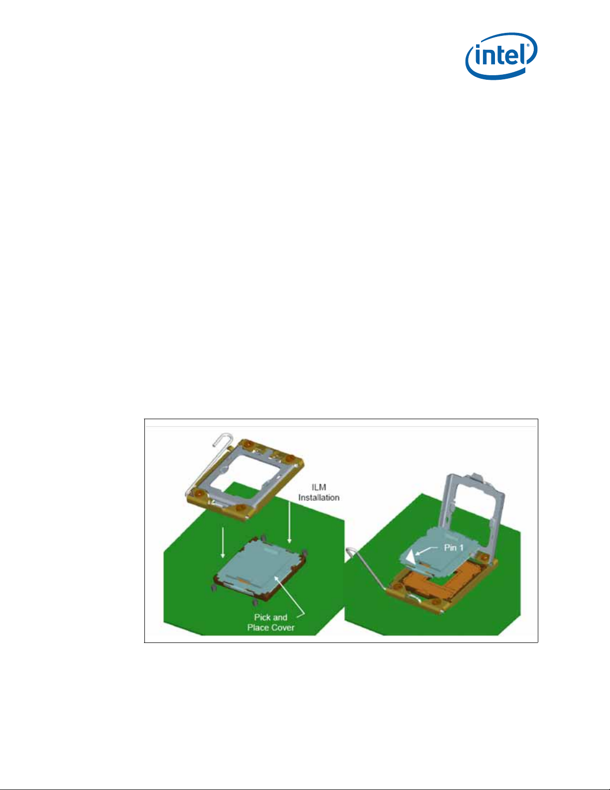
4 Independent Loading Mechanism (ILM)...................................................................26
4.1 Design Concept.................................................................................................26
4.1.1 ILM Cover Assembly Design Overview.......................................................26
4.1.2 ILM Back Plate Design Overview...............................................................27
4.2 Assembly of ILM to a Motherboard.......................................................................28
5 LGA1366 Socket and ILM Electrical, Mechanical and Environmental Specifications .. 31
5.1 Component Mass...............................................................................................31
5.2 Package/Socket Stackup Height ..........................................................................31
5.3 Socket Maximum Temperature............................................................................31
5.4 Loading Specifications.................................... .. .. ................................................33
5.4.1 Board Deflection Guidance.......................................................................33
5.5 Electrical Requirements......................................................................................34
5.6 Environmental Requirements ............................................................................ ..35
6 Thermal Specifications ............................................................................................36
6.1 Package Thermal Specifications...................................................... .. ...................36
6.1.1 Thermal Specifications ............................................................................36
6.1.2 Thermal Metrology .................................................................................47
6.2 Processor Thermal Features................................................................................48
6.2.1 Processor Temperature ...........................................................................48
6.2.2 Adaptive Thermal Monitor........................................................................48
August 2010 Thermal/Mechanical Design Guide
Order Number: 323107-002US 3
Intel® Xeon® Processor C5500/C3500 Series and LGA1366 Socket
Page 4

6.2.3 THERMTRIP# Signal...................................... ..........................................51
6.3 Platform Environment Control Interface (PECI)......................................................51
6.3.1 Introduction...........................................................................................51
6.3.2 PECI Specifications .................................................................................53
7Thermal Solutions....................................................................................................54
7.1 Performance Targets....................................................................... .. .. ...............54
7.2 Heat Pipe Considerations ....................................................................................56
7.3 Assembly..........................................................................................................57
7.3.1 Thermal Interface Material (TIM) ........................................... .. .. ... ............58
7.4 Structural Considerations....................................................................................58
7.5 Thermal Design........................................................... .. .. .......................... .. .. ....59
7.5.1 Thermal Characterization Parameter..........................................................59
7.5.2 NEBS Thermal Profile ..............................................................................60
7.5.3 Power Thermal Utility ..............................................................................61
7.6 Thermal Features..................... .......................... .. .. ......................... .. .. ...............61
7.6.1 Fan Speed Control ................................................ ... ......................... .. ....61
7.6.2 PECI Averaging and Catastrophic Thermal Management...............................62
7.6.3 Intel® Turbo Boost Technology............................................ .....................62
7.6.4 Absolute Processor Temperature...............................................................63
7.6.5 Custom Heat Sinks For UP ATCA...............................................................63
8 Quality and Reliability Requirements .......................................................................66
8.1 Use Conditions ..................................................................................................66
8.2 Intel Reference Component Validation ..................................................................67
8.2.1 Board Functional Test Sequence ...............................................................67
8.2.2 Post-Test Pass Criteria.............................................................................68
8.2.3 Recommended BIOS/Processor/Memory Test Procedures .............................68
8.3 Material and Recycling Requirements....................................................................68
A Component Suppliers...............................................................................................70
B Mechanical Drawings ...............................................................................................72
C Socket Mechanical Drawings....................................................................................89
Intel® Xeon® Processor C5500/C3500 Series and LGA1366 Socket
Thermal/Mechanical Design Guide August 2010
4 Order Number: 323107-002US
Page 5

Figures
1-1 Intel® Xeon® Processor C5500/C3500 Series Socket Stack-up .......................................8
2-1 Processor Package Assembly Sketch.........................................................................11
2-2 Processor Package Drawing (Sheet 1 of 2)............................................ .. .. ... ..............13
2-3 Processor Package Drawing (Sheet 2 of 2)............................................ .. .. ... ..............14
2-4 Processor Top-Side Markings ...................... .. ..................................................... ......16
2-5 Processor Land Coordinates and Quadrants, Bottom View................................ .. .. .. .. .. ..17
3-1 LGA1366 Socket with Pick and Place Cover Removed ..................................................18
3-2 LGA1366 Socket Contact Numbering (Top View of Socket)...........................................19
3-3 LGA1366 Socket Land Pattern (Top View of Board) .....................................................20
3-4 Attachment to Motherboard.....................................................................................21
3-5 Pick and Place Cover...............................................................................................22
3-6 Package Installation / Removal Features ...................................................................23
3-7 LGA1366 NCTF Solder Joints....................................................................................25
4-1 ILM Cover Assembly...............................................................................................27
4-2 Back Plate...................................... ......................... .. .. ......................... ... .. ............28
4-3 ILM Assembly........................................................................................................29
4-4 Pin1 and ILM Lever................................ .. .. ......................... ... ......................... ........30
5-1 Socket Temperature Measurement Location...............................................................32
5-2 Flow Chart of Knowledge-Based Reliability Evaluation Methodology...............................35
6-1 Intel
6-2 Intel® Xeon® Processor EC3539 and EC5539 Thermal Profile ...................................... 39
6-3 Intel
6-4 Intel® Xeon® Processor LC5518 Thermal Profile................................. .... .. .................. 42
6-5 Intel® Celeron® Processor P1053 Thermal Profile.......................................................43
6-6 Intel
6-7 Intel® Xeon® Processor LC3518 Thermal Profile................................. .... .. .................. 46
6-8 TTV Case Temperature (TCASE) Measurement Location...............................................47
6-9 Frequency and Voltage Ordering ..............................................................................49
7-1 1U Heatsink Performance Curves..............................................................................55
7-2 ATCA Heatsink Performance Curves..........................................................................56
7-3 TTV Die Size and Orientation ...................................................................................57
7-4 1U Reference Heatsink Assembly................................ .. .. .. ............................ .. .. .. ......57
7-5 Processor Thermal Characterization Parameter Relationships........................................59
7-6 NEBS Thermal Profile..............................................................................................60
7-7 UP ATCA Thermal Solution............................................... .. .......................... .. ..........64
7-8 UP ATCA System Layout....................... .. .. ......................... .. .......................... .. ........64
7-9 UP ATCA Heat Sink Drawing ....................................................................................65
B-1 Board Keepin / Keepout Zones (Sheet 1 of 4) ............................................................73
B-2 Board Keepin / Keepout Zones (Sheet 2 of 4) ............................................................74
B-3 Board Keepin / Keepout Zones (Sheet 3 of 4) ............................................................75
B-4 Board Keepin / Keepout Zones (Sheet 4 of 4) ............................................................76
B-5 1U Reference Heatsink Asse mb ly (She et 1 of 2).........................................................77
B-6 1U Reference Heatsink Asse mb ly (She et 2 of 2).........................................................78
B-7 1U Reference Heatsink Fin and Base (Sheet 1 of 2).....................................................79
B-8 1U Reference Heatsink Fin and Base (Sheet 2 of 2).....................................................80
B-9 Heatsink Shoulder Screw (1U, 2U, and Tower)...........................................................81
B-10 Heatsink Compression Spring (1U, 2U, and Tower) .....................................................82
B-11 Heatsink Retaining Ring (1U, 2U, and Tower).............................................................83
B-12 Heatsink Load Cup (1U, 2U, and Tower)....................................................................84
B-13 ATCA Reference Heatsink Assembly (Sheet 1 of 2)......................................................85
B-14 ATCA Reference Heatsink Assembly (Sheet 2 of 2)......................................................86
B-15 ATCA Reference Heatsink Fin and Base (Sheet 1 of 2).................................................87
B-16 ATCA Reference Heatsink Fin and Base (Sheet 2 of 2).................................................88
®
Xeon® Processor EC5549 and EC5509 Thermal Profile ....................................... 37
®
Xeon® Processor LC5528 Thermal Profile................................. .... .. .................. 40
®
Xeon® Processor LC3528 Thermal Profile................................. .... .. .................. 44
August 2010 Thermal/Mechanical Design Guide
Order Number: 323107-002US 5
Intel® Xeon® Processor C5500/C3500 Series and LGA1366 Socket
Page 6

C-1 Socket Mechanical Drawing - (Sheet 1 of 4)...............................................................90
C-2 Socket Mechanical Drawing - (Sheet 2 of 4)...............................................................91
C-3 Socket Mechanical Drawing - (Sheet 3 of 4)...............................................................92
C-4 Socket Mechanical Drawing - (Sheet 4 of 4)...............................................................93
Tables
1-1 Reference Documents ....................................................... .. .......................... .. .. ....... 9
1-2 Terms and Descriptions............................................................................................ 9
2-1 Processor Loading Specifications...............................................................................15
2-2 Package Handling Guidelines.................................... ................................................15
2-3 Processor Materials.................................................................................................16
5-1 Socket Component Mass..........................................................................................31
5-2 1366-land Package and LGA1366 Socket Stackup Height .............................................31
5-3 Socket and ILM Mechanical Specifications ..................................................................33
5-4 Electrical Requirements for LGA1366 Socket.................... .. .. .. .. .. ................................. 34
6-1 Intel
6-2 Intel
6-3 Intel® Xeon® Processor EC3539 and EC5539 Thermal Specifications ............................38
6-4 Intel® Xeon® Processor EC3539 and EC5539 Thermal Profile.......................................39
6-5 Intel
6-6 Intel® Xeon® Processor LC5528 Thermal Profile .........................................................41
6-7 Intel® Xeon® Processor LC5518 Thermal Specifications...............................................41
6-8 Intel
6-9 Intel® Celeron® Processor P1053 Thermal Specifications ................................ .............43
6-10 Intel® Celeron® Processor P1053 Thermal Profile................... .....................................43
6-11 Intel
6-12 Intel® Xeon® Processor LC3528 Thermal Profile .........................................................45
6-13 Intel® Xeon® Processor LC3518 Thermal Specifications...............................................45
6-14 Intel
6-15 GetTemp0() Error Codes..........................................................................................53
7-1 Boundary Conditions and Performance Targets ...........................................................54
7-2 Fan Speed Control, TCONTROL and DTS Relationship...................................................61
7-3 TCONTROL Guidance...............................................................................................62
8-1 Server Use Conditions Environment (System Level).....................................................66
8-2 Server Use Conditions Environment (System Level).....................................................67
A-1 Heatsinks and Thermal Interface Material ..................................................................70
A-2 LGA1366 Socket and ILM Components.......................................................................71
B-1 Mechanical Drawing List ..........................................................................................72
C-1 Mechanical Drawing List ..........................................................................................89
®
Xeon® Processor EC5549 and EC5509 Thermal Specifications .............................37
®
Xeon® Processor EC5549 and EC5509 Thermal Profile........................................38
®
Xeon® Processor LC5528 Thermal Specifications...............................................40
®
Xeon® Processor LC5518 Thermal Profile .........................................................42
®
Xeon® Processor LC3528 Thermal Specifications...............................................44
®
Xeon® Processor LC3518 Thermal Profile .........................................................46
Intel® Xeon® Processor C5500/C3500 Series and LGA1366 Socket
Thermal/Mechanical Design Guide August 2010
6 Order Number: 323107-002US
Page 7
Revision History
Revision Number Description Revision Date
002
001 First release February 2010
Modified Table 5-3, Socket and ILM Mechanical Specifications
Modified Section 7.6.1, Fan Speed Control
§ §
August 2010
August 2010 Thermal/Mechanical Design Guide
Order Number: 323107-002US 7
Intel® Xeon® Processor C5500/C3500 Series and LGA1366 Socket
Page 8

Heatsink
Socket and ILM
Back Plate
Introduction
1 Introduction
This document provides guidelines for the design of thermal and mechanical solutions
for processors in the Picket Post platform. The components described in this document
include:
• The processor thermal solution (heatsink) and associated retention hardware.
• The LGA1366 socket and the Independent Loading Mechanism (ILM) and back
plate.
®
Figure 1-1. Intel
Xeon® Processor C5500/C3500 Series Socket Stack-up
August 2010 Thermal/Mechanical Design Guide
Order Number: 323107-002US 8
The goals of this document are:
• To assist board and system thermal mechanical designers.
• To assist designers and suppliers of processor heatsinks.
Other processor specifications are provided in the Intel® Xeon® Processor C5500/
C3500 Series Datasheet.
Intel® Xeon® Processor C5500/C3500 Series and LGA1366 Socket
Page 9
1.1 Reference Documents
Material and concepts in the following documents may be beneficial when reading this
document.
Table 1-1. Reference Documents
Document Document# Notes
European Blue Angel Recycling Standards 3
®
Intel
Xeon® Processor C5500/C3500 Series Datasheet, Volume 1 323103 1
®
Intel
Xeon® Processor C5500/C3500 Series Datasheet, Volume 2 323317 1
®
Intel
Xeon® Processor 5500 Series Mechanical Model 321326 2
®
Intel
Xeon® Processor 5500 Series Thermal Model 321327 2
Entry-level Electronics Bay Specification 4
Notes:
1. See http://developer.intel.com/design/intarch/xeon5000/documentation.htm
2. See http://www.intel.com/p/en_US/products/server/processor/xeon5000/tools
3. Available at http://www.blauer-engel.de
4. Available at http://ssiforum.oaktree.com/
Introduction
1.2 Definition of Terms
Table 1-2. Terms and Descriptions (Sheet 1 of 2)
Term Description
Bypass Bypass is the area between a passive heatsink and any object that can act to form a
DTS Digital Thermal Sensor reports a relative die temperature as an offset from TCC
FSC Fan Speed Control
IHS Integrated Heat Spreader: a component of the processor package used to enhance the
ILM Independent Loading Mechanism provides the force needed to seat the 1366-LGA land
IMON The current monitor input to the CPU. The VRM tells the CPU how much current it is
LGA1366 socket The processor mates with the system board through this surface mount, 1366-land
PECI The Platform Environment Control Interface (PECI) is a one- wire interfac e that p rovid es
Ψ
CA
Ψ
CS
Ψ
SA
T
CASE
T
CASE_MAX
duct. For this example, it can be expressed as a dimension away from the outside
dimension of the fins to the nearest surface.
activation temperature.
thermal performance of the package. Component thermal solutions interface with the
processor at the IHS surface.
package onto the socket contacts.
drawing.
socket.
a communication channel between Intel processor and chipset components to external
monitoring devices.
Case-to-ambient thermal characterization parameter (psi). A measure of thermal
solution performance using t otal package power. Defined as (T
Package Power. Heat source should always be specified for Ψ measurements.
Case-to-sink thermal characterization parameter. A measure of thermal interface
material performance using total package po wer. D efined as (T
Package Power.
Sink-to-ambient thermal characterization parameter. A measure of heatsink thermal
performance using total package power. Defined as (T
The case temperature of the processor , measured at the geometric center of the topside
of the IHS.
The maximum case temperature as specified in a component specification.
– TLA) / Total
CASE
– TS) / Total
CASE
– TLA) / Total Package Power.
S
®
Xeon® Processor C5500/C3500 Series and LGA1366 Socket
Intel
Thermal/Mechanical Design Guide August 2010
9 Order Number: 323107-002US
Page 10
Introduction
Table 1-2. Terms and Descriptions (Sheet 2 of 2)
Term Description
TCC Thermal Control Circuit: Thermal monitor uses the TCC to reduce the die temperature
T
CONTROL
TDP Thermal Design Power: Thermal solution must be designed to dissipate this target
Thermal Monitor A power reduction feature designed to decrease temperature after the processor has
Thermal Profile Line that defines case temperature specification of a processor at a given power level.
TIM Thermal Interface Material: The thermally conductive compound between the heatsink
T
LA
T
SA
U A unit of measure used to define server rack spacing height. 1U is equal to 1.75 in, 2U
by using clock modulation and/or operating frequency and input voltage adjustment
when the die temperature is very near its operating limits.
T
is a static value below TCC activation used as a trigger point for fan speed
control
control.
power level. TDP is not the maximum power that the processor can dissipate.
reached its maximum operating temperature.
and the processor case. This material fills the air gaps and voids, and enhances the
transfer of the heat from the processor case to the heatsink.
The measured ambient temperature locally surrounding the proc essor. The ambient
temperature should be measured just upstream of a p assive heatsink o r at the fan inlet
for an active heatsink.
The system ambient air temperature external to a system chassis. This temperature is
usually measured at the chassis air inlets.
equals 3.50 in, etc.
§
August 2010 Thermal/Mechanical Design Guide
Order Number: 323107-002US 10
Intel® Xeon® Processor C5500/C3500 Series and LGA1366 Socket
Page 11
IHS
Substrate
LGA1366 Socket
System Board
Capacitors
TIM
IHS
Substrate
LGA
System Board
Capacitors
Die
TIM
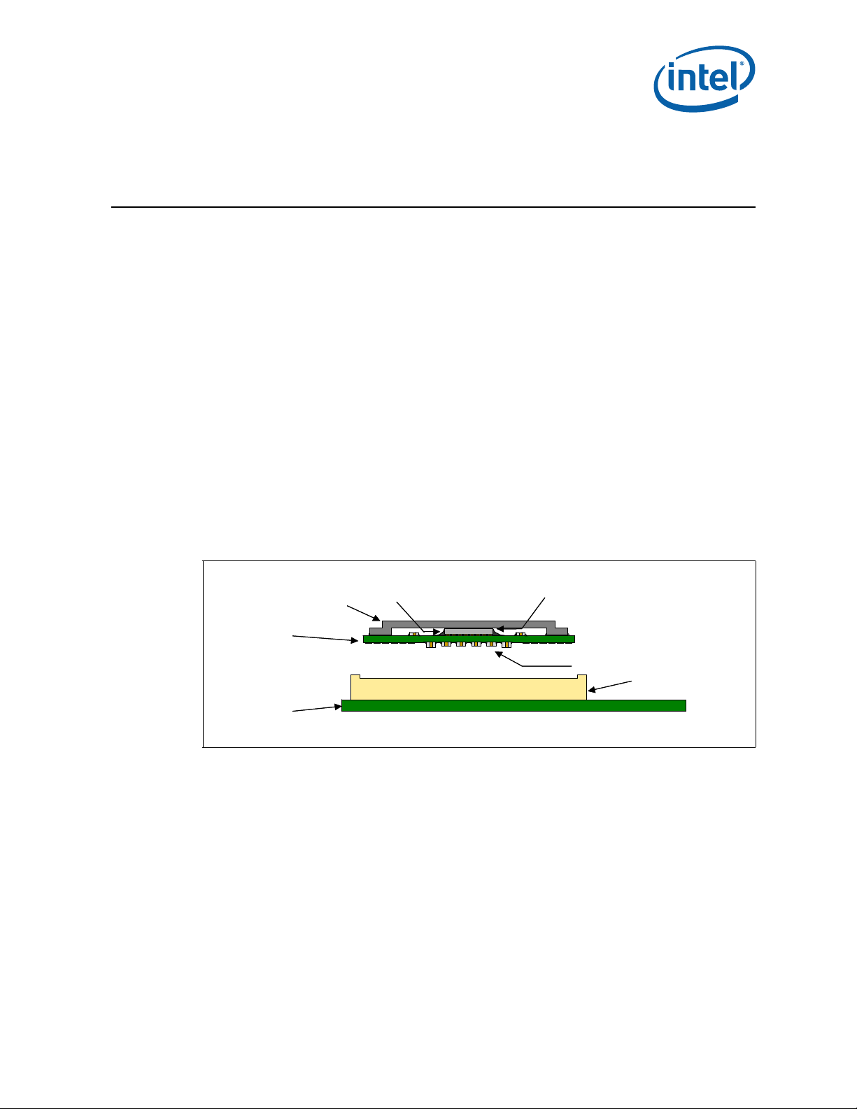
Package Mechanical Specifications
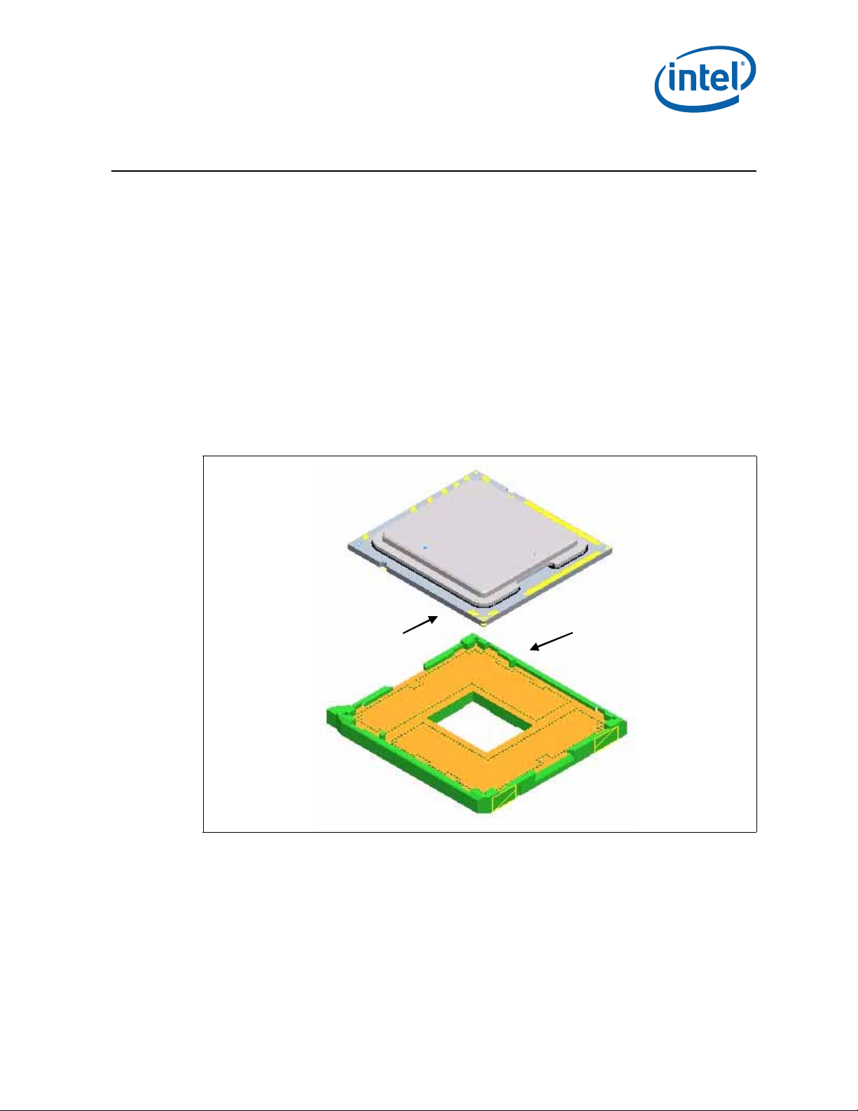
2 Package Mechanical
Specifications
2.1 Package Mechanical Specifications
The processor is packaged in a Flip-Chip Land Grid Array (FC-LGA6) package that
interfaces with the motherboard via an LGA1366 socket. The package consists of a
processor mounted on a substrate land-carrier. An integrated heat spreader (IHS) is
attached to the package substrate and core and serves as the mating surface for
processor component thermal solutions, such as a heatsink. Figure 2-1 shows a sketch
of the processor package components and how they are assembled together. See
Section 3 and Section 4.
The package components shown in Figure 2-1 include the following:
• Integrated Heat Spreader (IHS)
• Thermal Interface Material (TIM)
• Processor core (die)
• Package substrate
• Capacitors
Figure 2-1. Processor Package Assembly Sketch
Note:
1. Socket and motherboard are included for reference and are not part of processor package.
August 2010 Thermal/Mechanical Design Guide
Order Number: 323107-002US 11
Intel® Xeon® Processor C5500/C3500 Series and LGA1366 Socket
Page 12

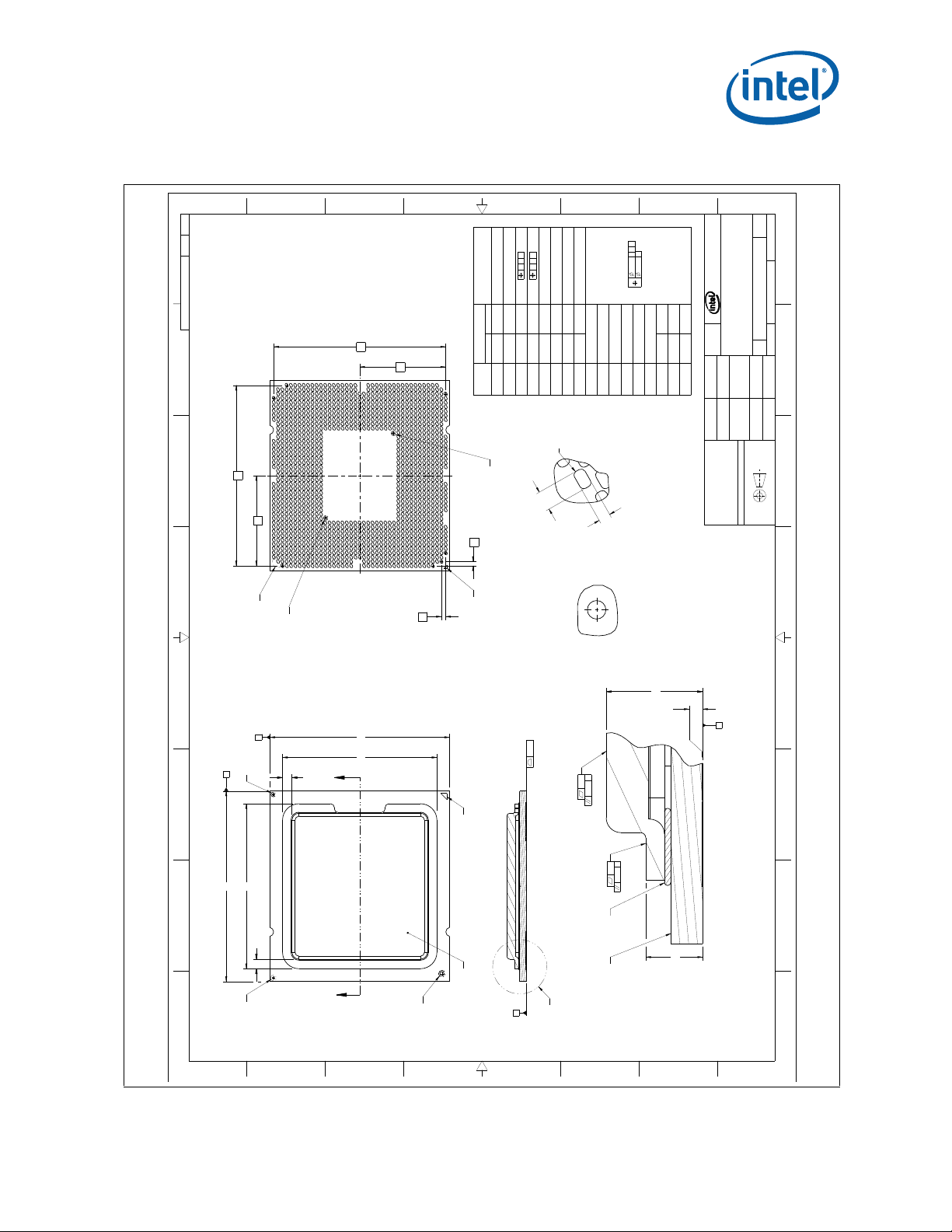
2.1.1 Package Mechanical Drawing
The package mechanical drawings are shown in Figure 2-2 and Figure 2-3. The
drawings include dimensions necessary to design a thermal solution for the processor.
These dimensions include:
1. Package reference with tolerances (total height, length, width, etc.)
2. IHS parallelism and tilt
3. Land dimensions
4. Top-side and back-side component keep-out dimensions
5. Reference datums
6. All drawing dimensions are in mm
Package Mechanical Specifications
®
Xeon® Processor C5500/C3500 Series and LGA1366 Socket
Intel
Thermal/Mechanical Design Guide August 2010
12 Order Number: 323107-002US
Page 13
8 7 6 5 4 3 2
H
G
F
E
D
C
B
A
8 7 6 5 4 3 2 1
H
G
F
E
D
C
B
A
A
A
R
D
E
C
C
4X RM
1
M
2
M
3
F
4
F
2
B1C
1
C
3
B
2
C
2
C
4
G
2
G
1
H
1
H
2
J
1
J
2
0.02
THIS DRAWING CONTAINS INTEL CORPORATION CONFIDENTIAL INFORMATION. IT IS DISCLOSED IN CONFIDENCE AND ITS CONTENTS
MAY NOT BE DISCLOSED, REPRODUCED, DISPLAYED OR MODIFIED, WITHOUT THE PRIOR WRITTEN CONSENT OF INTEL CORPORATION.
D76126 1 7
DWG. NO SHT. REV
THIS DRAWING CONTAINS INTEL CORPORATION CONFIDENTIAL INFORMATION. IT IS DISCLOSED IN CONFIDENCE AND ITS CONTENTS
MAY NOT BE DISCLOSED, REPRODUCED, DISPLAYED OR MODIFIED, WITHOUT THE PRIOR WRITTEN CONSENT OF INTEL CORPORATION.
D76126 1 7
DWG. NO SHT. REV
DEPARTMENT
2200 MISSION COLLEGE BLVD.
P.O. BOX 58119
SANTA CLARA, CA 95052-8119
TITLE
EMTS DRAWING
SIZE DRAWING NUMBER REV
A1 D76126 7
SCALE: 2:1
DO NOT SCALE DRAWING
SHEET 1 OF 2
FINISHMATERIAL
DATEAPPROVED BY
DATECHECKED BY
DATEDRAWN BY
DATEDESIGNED BY
UNLESS OTHERWISE SPECIFIED
INTERPRET DIMENSIONS AND TOLERANCES
IN ACCORDANCE WITH ASME Y14.5M-1994
DIMENSIONS ARE IN MILLIMETERS
ALL UNTOLERANCED LINEAR
DIMENSIONS ±0
ANGLES ±0.5
THIRD ANGLE PROJECTION
SEE DETAIL B
SEE DETAIL B
SEE DETAIL B
SEE DETAIL B
IHS LID
SEE DETAIL B
PIN 1
SEE DETAIL C
PIN 1
BAAY AWAV AU
AT
ARAP ANAM ALAK AJAH AGAF AEAD ACAB AAY WV UT RP NM LK JH GF ED CB A
1 3 5 7 9 11 13 15 17 19 21 23 25 27 29 31 33 35 37 39 41 43
2 4 6 8 10 12 14 16 18 20 22 24 26 28 30 32 34 36 38 40 42
SEE DETAIL A
SECTION A-A
DETAIL A
SCALE 20:1
PACKAGE SUBSTRATE IHS SEALANT
IHS LID
DETAIL
C
SCALE 20:1
DETAIL B
SUBSTRATE ALIGNMENT FIDUCIAL
X5
SCALE 35:1
SYMBOL
MILLIMETERS
COMMENTS
MIN MAX
B
1
44.93 45.07
B
2
42.43 42.57
C
1
38.9 39.1
1CE
C
2
36.4 36.6
1CD
C
3
2.2 2.3
C
4
2.2 2.3
F
2
4.377 4.757
F
4
2.498 2.896
G
1
42.672 BASIC
G
2
40.64 BASIC
H
1
21.336 BASIC
H
2
20.32 BASIC
J
1
1.016 BASIC
J
2
1.016 BASIC
M
1
0.19 0.23
M
2
0.88 0.96
M
3
0.53 0.61
0.203
0.08
0.203 C
0.203 C D E
0.071 C
0.05
0.203 C
Package Mechanical Specifications
Figure 2-2. Processor Package Drawing (Sheet 1 of 2)
August 2010 Thermal/Mechanical Design Guide
Order Number: 323107-002US 13
Intel® Xeon® Processor C5500/C3500 Series and LGA1366 Socket
Page 14
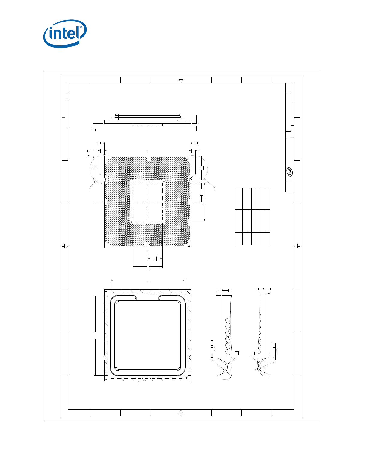
Figure 2-3. Processor Package Drawing (Sheet 2 of 2)
H
G
F
E
D
C
B
A
H
G
F
E
D
C
B
A
8 7 6 5 4 3 2
8 7 6 5 4 3 2 1
R
H
H
H
C
9.455
7.2
1.06 MAX
COMPONENT HEIGHT
T
1
T
2
V
1
V
2
2X 36.5
2X 39
14.4
18.91
E
G
E
G
THIS DRAWING CONTAINS INTEL CORPORATION CONFIDENTIAL INFORMATION. IT IS DISCLOSED IN CONFIDENCE AND ITS CONTENTS
MAY NOT BE DISCLOSED, REPRODUCED, DISPLAYED OR MODIFIED, WITHOUT THE PRIOR WRITTEN CONSENT OF INTEL CORPORATION.
THIS DRAWING CONTAINS INTEL CORPORATION CONFIDENTIAL INFORMATION. IT IS DISCLOSED IN CONFIDENCE AND ITS CONTENTS
MAY NOT BE DISCLOSED, REPRODUCED, DISPLAYED OR MODIFIED, WITHOUT THE PRIOR WRITTEN CONSENT OF INTEL CORPORATION.
D76126 2 7
DWG. NO SHT. REV
DEPARTMENT
2200 MISSION COLLEGE BLVD.
P.O. BOX 58119
SANTA CLARA, CA 95052-8119
SIZE DRAWING NUMBER REV
A1 D76126 7
SCALE: 2:1
DO NOT SCALE DRAWING
SHEET 2 OF 2
1 3 5 7 9 11 13 15 17 19 21 23 25 27 29 31 33 35 37 39 41 43
2 4 6 8 10 12 14 16 18 20 22 24 26 28 30 32 34 36 38 40 42
SEE DETAIL D
SEE DETAIL E
BAAY AWAV AU
AT
ARAP ANAM ALAK AJAH AGAF AEAD ACAB AAY WV UT RP NM LK JH GF ED CB A
DETAIL D
SCALE 15:1
0.23 C H E
M N
NM
R
2
DETAIL
E
SCALE 15:1
0.23 C H G
J K
KJ
R
1
4X
SURFACE
TEST PAD AREA
SYMBOL
MILLIMETERS
COMMENTS
MIN MAX
R
1
R1.09 --
R
2
R1.09 --
T
1
0.2 --
T
2
11.7 --
V
1
0.2 --
V
2
11.7 --
Package Mechanical Specifications
®
Xeon® Processor C5500/C3500 Series and LGA1366 Socket
Intel
Thermal/Mechanical Design Guide August 2010
14 Order Number: 323107-002US
Page 15
Package Mechanical Specifications
2.1.2 Processor Component Keep-Out Zones
The processor may contain components on the substrate that define component
keep-out zone requirements. A thermal and mechanical solution design must not
intrude into the required keep-out zones. Do not contact the Test Pad Area with
conductive material. Decoupling capacitors are typically mounted to either the topside
or land-side of the package substrate. See Figure 2-2 and Figure 2-3 for keep-out
zones. The location and quantity of package capacitors may change due to
manufacturing efficiencies but will remain within the component keep-in.
2.1.3 Package Loading Specifications
Table 2-1 provides load specifications for the processor package. These maximum
limits should not be exceeded during heatsink assembly, shipping conditions, or
standard use condition. Exceeding these limits during test may result in component
failure. The processor substrate should not be used as a mechanical reference or load-
.
Table 2-1. Processor Loading Specifications
bearing surface for thermal solutions.
Parameter Maximum Notes
Static Compressive Load 890 N [200 lbf] 1, 2, 3
Dynamic Compressive Load 1779 N [400 lbf] [max static
compressive + dynamic load]
1, 3, 4
Notes:
1. These specifications apply to uniform compressive loading in a direction normal to the processor IHS.
2. This is the maximum static force that can be applied by the heatsink and Independent Loading Mechanism
(ILM).
3. These specifications are based on limited testing for design characterization. Loading limits are for the
package constrained by the limits of the processor socket.
4. Dynamic loading is defined as an 11 ms duration average load superimposed on the static load
requirement.
2.1.4 Package Handling Guidelines
Table 2-2 includes a list of guidelines on package handling in terms of recommended
maximum loading on the processor IHS relative to a fixed substrate. These package
handling loads may be experienced during heatsink removal.
Table 2-2. Package Handling Guidelines
Parameter Maximum Recommended
Shear 70 lbs
Tensile 25 lbs
Torque 35 in.lbs
2.1.5 Package Insertion Specifications
The processor can be inserted into and removed from a LGA1366 socket 15 times. The
socket should meet the LGA1366 requirements detailed in Section 5.
August 2010 Thermal/Mechanical Design Guide
Order Number: 323107-002US 15
Intel® Xeon® Processor C5500/C3500 Series and LGA1366 Socket
Page 16
2.1.6 Processor Mass Specification
GRP1LINE1
GRP1LINE2
G2L1
G2L2
G3L1
G3L2
Legend: Mark Text (Engineering Mark):
GRP1LINE1: INTEL{M}{C}’YY
GRP1LINE2: INTEL CONFIDENTIAL
GRP1LINE3: QDF ES XXXXX
GRP1LINE4: FORECAST-NAME
GRP1LINE5: {FPO} {e4}
Legend: Mark Text (Production Mark):
GRP1LINE1: INTEL{M}{C}’YY PROC#
GRP1LINE2: SUB-BRAND
GRP1LINE3: SSPEC XXXXX
GRP1LINE4: SPEED/CACHE/INTC
GRP1LINE5: {FPO} {e4}
The typical mass of the processor is 35 grams. This mass [weight] includes all the
components that are included in the package.
2.1.7 Processor Materials
Package Mechanical Specifications
Table 2-3 lists some of the package components and associated materials.
Table 2-3. Processor Materials
Component Material
Integrated Heat Spreader (IHS) Nickel Plated Copper
Substrate Fiber Reinforced Resin
Substrate Lands Gold Plated Copper
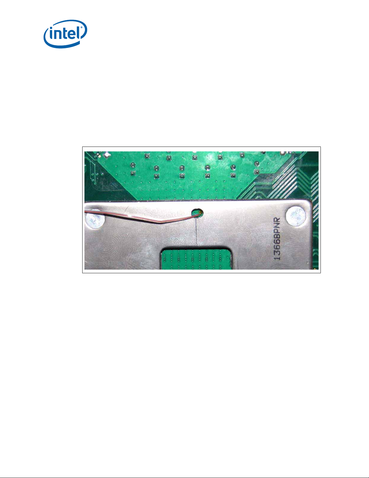
2.1.8 Processor Markings
Figure 2-4 shows the topside markings on the processor. This diagram is to aid in the
identification of the processor.
Figure 2-4. Processor Top-Side Markings
®
Xeon® Processor C5500/C3500 Series and LGA1366 Socket
Intel
Thermal/Mechanical Design Guide August 2010
16 Order Number: 323107-002US
Page 17
Package Mechanical Specifications
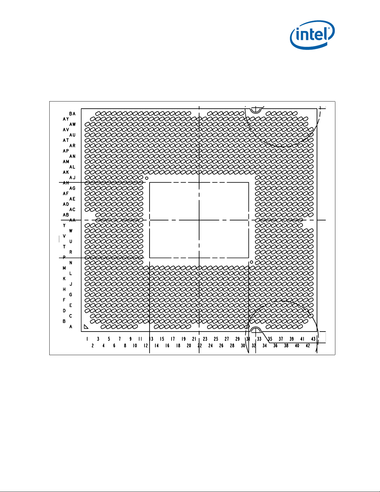
2.1.9 Processor Land Coordinates
Figure 2-5 shows the bottom view of the processor land coordinates. The coordinates
.
Figure 2-5. Processor Land Coordinates and Quadrants, Bottom View
are referred to throughout the document to identify processor lands.
§
August 2010 Thermal/Mechanical Design Guide
Order Number: 323107-002US 17
Intel® Xeon® Processor C5500/C3500 Series and LGA1366 Socket
Page 18
socket
cavity
package socket
cavity
package
LGA1366 Socket
3 LGA1366 Socket
This section describes a surface mount, LGA (Land Grid Array) socket intended for the
Intel® Xeon® processor C5500/C3500 series in the Picket Post platform. The socket
provides I/O, power and ground contacts. The socket contains 1366 contacts arrayed
about a cavity in the center of the socket with lead-free solder balls for surface
mounting on the motherboard.
The socket has 1366 contacts with 1.016 mm X 1.016 mm pitch (X by Y) in a 43 x 41
grid array with 21 x 17 grid depopulation in the center of the array and selective
depopulation elsewhere.
The socket must be compatible with the package (processor) and the Independent
Loading Mechanism (ILM). The design includes a back plate which is integral to having
a uniform load on the socket solder joints. Socket loading specifications are listed in
Section 5.
Figure 3-1. LGA1366 Socket with Pick and Place Cover Removed
August 2010 Thermal/Mechanical Design Guide
Order Number: 323107-002US 18
Intel® Xeon® Processor C5500/C3500 Series and LGA1366 Socket
Page 19

Figure 3-2. LGA1366 Socket Contact Numbering (Top View of Socket)
LGA1366 Socket
®
Xeon® Processor C5500/C3500 Series and LGA1366 Socket
Intel
Thermal/Mechanical Design Guide August 2010
19 Order Number: 323107-002US
Page 20
A C E G J L N R U W AA AC AE AG AJ AL AN AR AU AW BA
B D F H K M P T V Y AB AD AF AH AK AM AP AT AV AY BB
1
3
7
5
9
11
15
13
17
19
23
21
25
27
31
29
1
3
7
5
9
11
15
13
17
19
23
21
25
27
31
29
2
8
4
6
10
16
12
14
18
24
20
22
26
32
28
30
2
8
4
6
10
16
12
14
18
24
20
22
26
32
28
30
16
12
15
13
14
17
18
24
20
19
23
21
22
25
26
32
28
27
31
29
30
33
34
40
36
35
39
37
38
41
42
43
LGA1366 Socket
3.1 Board Layout
The land pattern for the LGA1366 socket is 40 mils X 40 mils (X by Y), and the pad size
is 18 mils. There is no round-off (conversion) error between socket pitch (1.016 mm)
and board pitch (40 mil) because these values are equivalent.
In general, metal defined (MD) pads perform better than solder mask defined (SMD)
pads under thermal cycling, and SMD pads perform better than MD pads under
dynamic stress. Recommendations for pad definition on a per pad basis do not exist for
the LGA1366 socket.
The 40 mil spacing results in a reduced drill keepout as compared to previous
platforms. Drill keepout is explained in section 3.2.1 of the Intel
Design Guide (PDG). Select PCB suppliers are capable of producing 40 mil spacing.
Figure 3-3. LGA1366 Socket Land Pattern (Top View of Board)
August 2010 Thermal/Mechanical Design Guide
Order Number: 323107-002US 20
®
Xeon® 5500 Platform
Intel® Xeon® Processor C5500/C3500 Series and LGA1366 Socket
Page 21
3.2 Attachment to Motherboard
The socket is attached to the motherboard by 1366 solder balls. There are no additional
external methods (i.e. screw, extra solder, adhesive, etc.) to attach the socket. As
indicated in Figure 3-4, the Independent Loading Mechanism (ILM) is not present
during the attach (reflow) process.
Figure 3-4. Attachment to Motherboard
LGA1366 Socket
3.3 Socket Components
The socket has two main components, the socket body and Pick and Place (PnP) cover,
and is delivered as a single integral assembly. See Appendix C for detailed drawings.
3.3.1 Socket Body Housing
The housing material is thermoplastic or equivalent with UL 94 V -0 flame rating capable
of withstanding 260°C for 40 seconds (typical reflow/rework). The socket coefficient of
thermal expansion (in the XY plane), and creep properties, must be such that the
integrity of the socket is maintained for the conditions listed in Section 8.
The color of the housing will be dark as compared to the solder balls. This provides the
contrast needed for pick and place vision systems.
3.3.2 Solder Balls
A total of 1366 solder balls corresponding to the contacts are on the bottom of the
socket for surface mounting with the motherboard.
The socket has the following solder ball material:
• Lead free SAC (SnAgCu) solder alloy with a silver (Ag) content between 3% and
4% and a melting temperature of approximately 217°C. The alloy must be
compatible with immersion silver (ImAg) motherboard surface finish and a SAC
alloy solder paste.
The co-planarity (profile) and true position requirements are defined in Appendix C.
®
Xeon® Processor C5500/C3500 Series and LGA1366 Socket
Intel
Thermal/Mechanical Design Guide August 2010
21 Order Number: 323107-002US
Page 22
LGA1366 Socket
3.3.3 Contacts
Base material for the contacts is high strength copper alloy.
For the area on socket contacts where processor lands will mate, there is a 0.381 μm
[15 μinches] minimum gold plating over 1.27 μm [50 μinches] minimum nickel
underplate.
No contamination by solder in the contact area is allowed during solder reflow.
3.3.4 Pick and Place Cover
The cover provides a planar surface for vacuum pick up used to place components in
the Surface Mount Technology (SMT) manufacturing line. The cover remains on the
socket during reflow to help prevent contamination during reflow. The cover can
withstand 260° C for 40 seconds (typical reflow/rework profile) and the conditions
listed in Section 6 without degrading.
As indicated in Figure 3-5, the cover remains on the socket during ILM installation, and
should remain on whenever possible to help prevent damage to the socket contacts.
Cover retention must be sufficient to support the socket weight during lifting,
translation, and placement (board manufacturing), and during board and system
shipping and handling.
The covers are designed to be interchangeable between socket suppliers. As indicated
in Figure 3-5, a Pin1 indicator on the cover provides a visual reference for proper
orientation with the socket.
Figure 3-5. Pick and Place Cover
August 2010 Thermal/Mechanical Design Guide
Order Number: 323107-002US 22
Intel® Xeon® Processor C5500/C3500 Series and LGA1366 Socket
Page 23

3.4 Package Installation / Removal
alignment
walls
orientation
notch
orientation
post
access
Pin1 triangle
Pin1 chamfer
alignment
walls
orientation
notch
orientation
post
access
Pin1 triangle
Pin1 chamfer
As indicated in Figure 3-6, access is provided to facilitate manual installation and
removal of the package.
To assist in package orientation and alignment with the socket:
• The package Pin1 triangle and the socket Pin1 chamfer provide visual reference for
proper orientation.
• The package substrate has orientation notches along two opposing edges of the
package, offset from the centerline. The socket has two corresponding orientation
posts to physically prevent mis-orientation of the package. These orientation
features also provide initial rough alignment of package to socket.
• The socket has alignment walls at the four corners to provide final alignment of the
.
Figure 3-6. Package Installation / Removal Features
package.
LGA1366 Socket
3.4.1 Socket Standoffs and Package Seating Plane
Intel
Thermal/Mechanical Design Guide August 2010
23 Order Number: 323107-002US
Standoffs on the bottom of the socket base establish the minimum socket height after
solder reflow and are specified in Appendix C.
Similarly, a seating plane on the topside of the socket establishes the minimum
package height. See Section 5.2 for the calculated IHS height above the motherboard.
®
Xeon® Processor C5500/C3500 Series and LGA1366 Socket
Page 24

LGA1366 Socket
3.5 Durability
The socket must withstand 30 cycles of processor insertion and removal. The max
chain contact resistance from Table 5-4 must be met when mated in the 1st and 30th
cycles.
The socket Pick and Place cover must withstand 15 cycles of insertion and removal.
3.6 Markings
There are three markings on the socket:
• LGA1366: Font type is Helvetica Bold - minimum 6 point (2.125 mm).
• Manufacturer's insignia (font size at supplier's discretion).
• Lot identification code (allows traceability of manufacturing date and location).
All markings must withstand 260° C for 40 seconds (typical reflow/rework profile)
without degrading, and must be visible after the socket is mounted on the
motherboard.
LGA1366 and the manufacturer's insignia are molded or laser marked on the side wall.
3.7 Component Insertion Forces
Any actuation must meet or exceed SEMI S8-95 Safety Guidelines for Ergonomics/
Human Factors Engineering of Semiconductor Manufacturing Equipment, example T able
R2-7 (Maximum Grip Forces). The socket must be designed so that it requires no force
to insert the package into the socket.
3.8 Socket Size
Socket information needed for motherboard design is given in Appendix C.
This information should be used in conjunction with the reference motherboard keep-
out drawings provided in Appendix B to ensure compatibility with the reference thermal
mechanical components.
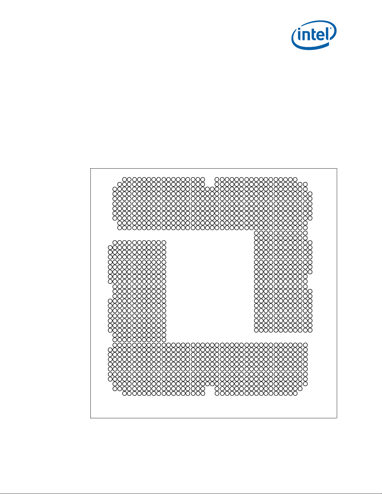
3.9 LGA1366 Socket NCTF Solder Joints
Intel has defined selected solder joints of the socket as non-critical to function (NCTF)
when evaluating package solder joints post environmental testing. The processor
signals at NCTF locations are typically redundant ground or non-critical reserved, so the
loss of the solder joint continuity at end of life conditions will not affect the overall
product functionality. Figure 3-7 identifies the NCTF solder joints.
August 2010 Thermal/Mechanical Design Guide
Order Number: 323107-002US 24
Intel® Xeon® Processor C5500/C3500 Series and LGA1366 Socket
Page 25
.
A C E G J L N R U W AA AC AE AG AJ AL AN AR AU AW BA
B D F H K M P T V Y AB AD AF AH AK AM AP AT AV AY BB
1
3
7
5
9
11
15
13
17
19
23
21
25
27
31
29
1
3
7
5
9
11
15
13
17
19
23
21
25
27
31
29
2
8
4
6
10
16
12
14
18
24
20
22
26
32
28
30
2
8
4
6
10
16
12
14
18
24
20
22
26
32
28
30
16
12
15
13
14
17
18
24
20
19
23
21
22
25
26
32
28
27
31
29
30
33
34
40
36
35
39
37
38
41
42
43
Figure 3-7. LGA1366 NCTF Solder Joints
LGA1366 Socket
Note: For platforms supporting the DP processor land C3 is CTF.
®
Xeon® Processor C5500/C3500 Series and LGA1366 Socket
Intel
Thermal/Mechanical Design Guide August 2010
25 Order Number: 323107-002US
§
Page 26

Independent Loading Mechanism (ILM)
4 Independent Loading
Mechanism (ILM)
The Independent Loading Mechanism (ILM) provides the force needed to seat the
1366-LGA land package onto the socket contacts. The ILM is physically separate from
the socket body. The assembly of the ILM is expected to occur after wave solder. The
exact assembly location is dependent on manufacturing preference and test flow. See
the Manufacturing Advantage Service collateral for this platform for additional
guidance.
Note: The ILM has two critical functions: deliver the force to seat the processor onto the
socket contacts and distribute the resulting load evenly through the socket solder
joints.
Note: The mechanical design of the ILM is integral to the overall functionality of the LGA1366
socket. Intel performs detailed studies on integration of processor package, socket and
ILM as a system. These studies directly impact the design of the ILM. The Intel
reference ILM will be “build to print” from Intel controlled drawings. Intel recommends
using the Intel Reference ILM. Custom non-Intel ILM designs do not benefit from Intel's
detailed studies and may not incorporate critical design parameters.
4.1 Design Concept
The ILM consists of two assemblies that will be procured as a set from the enabled
vendors. These two components are ILM cover assembly and back plate.
4.1.1 ILM Cover Assembly Design Overview
The ILM cover assembly consists of four major pieces: load lever, load plate, frame and
the captive fasteners.
The load lever and load plate are stainless steel. The frame and fasteners are high
carbon steel with appropriate plating. The fasteners are fabricated from a high carbon
steel. The frame provides the hinge locations for the load lever and load plate.
The cover assembly design ensures that once assembled to the back plate and the load
lever is closed, the only features touching the board are the captive fasteners. The
nominal gap of the frame to the board is ~1 mm when the load plate is closed on the
empty socket or when closed on the processor package.
When closed the load plate applies two point loads onto the IHS at the “dimpled”
features shown in Figure 4-1. The reaction force from closing the load plate is
transmitted to the frame and through the captive fasteners to the back plate. Some of
the load is passed through the socket body to the board inducing a slight compression
on the solder joints.
August 2010 Thermal/Mechanical Design Guide
Order Number: 323107-002US 26
Intel® Xeon® Processor C5500/C3500 Series and LGA1366 Socket
Page 27
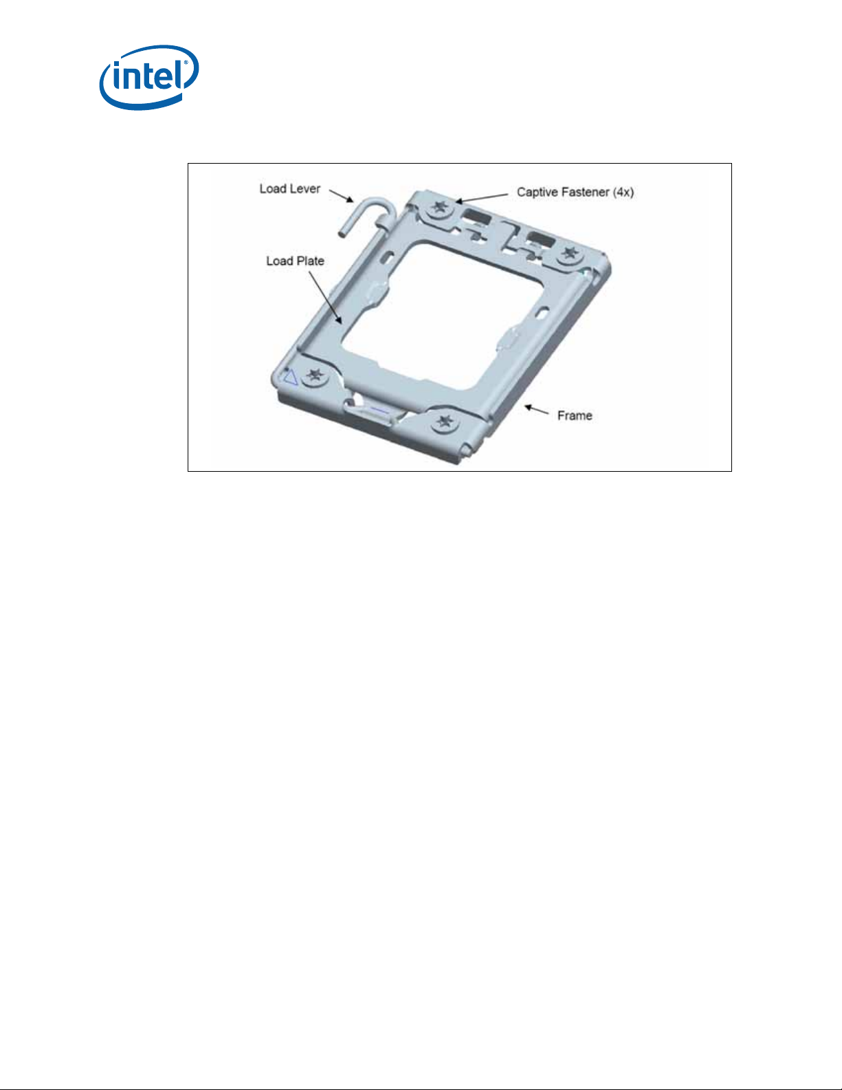
Figure 4-1. ILM Cover Assembly
Independent Loading Mechanism (ILM)
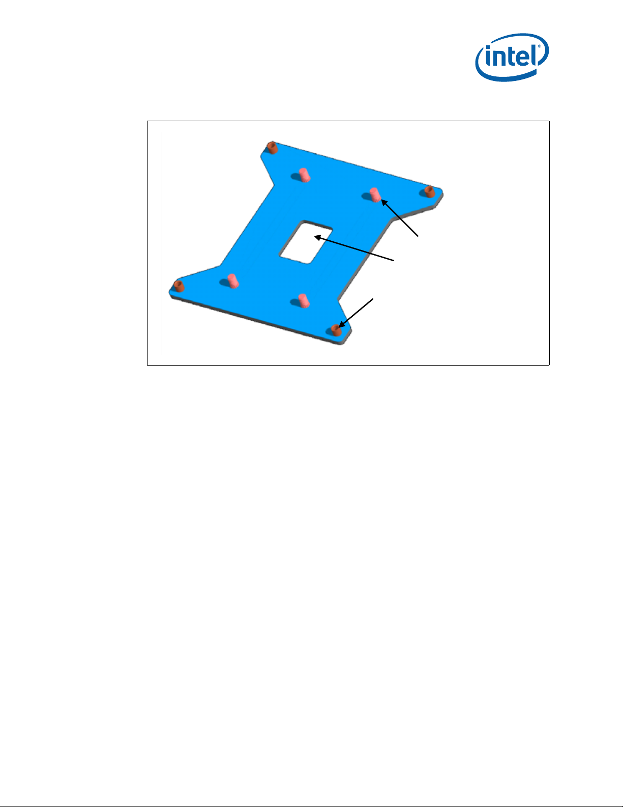
4.1.2 ILM Back Plate Design Overview
The unified back plate for 2-socket server and 2-socket Workstation products consists
of a flat steel back plate with threaded studs for ILM attach, and internally threaded
nuts for heatsink attach. The threaded studs have a smooth surface feature that
provides alignment for the back plate to the motherboard for proper assembly of the
ILM around the socket. A clearance hole is located at the center of the plate to allow
access to test points and backside capacitors. An additional cut-out on two sides
provides clearance for backside voltage regulator components. An insulator is preapplied.
Back plates for processors in 1-socket workstation platforms are covered in the Intel
®
Processor 3500 Series Thermal/Mechanical Design Guide.
Xeon
®
®
Xeon® Processor C5500/C3500 Series and LGA1366 Socket
Intel
Thermal/Mechanical Design Guide August 2010
27 Order Number: 323107-002US
Page 28
Threaded studs
Threaded nuts
Clearance hole
C
u
t
-
o
u
t
Threaded studs
Threaded nuts
Clearance hole
C
u
t
-
o
u
t
C
u
t
-
o
u
t
Threaded studs
Clearance hole
Threaded nuts
Independent Loading Mechanism (ILM)
Figure 4-2. Back Plate
4.2 Assembly of ILM to a Motherboard
The ILM design allows a bottoms up assembly of the components to the board. In
step 1 (see Figure 4-3), the back plate is placed in a fixture. Holes in the motherboard
provide alignment to the threaded studs. In step 2, the ILM cover assembly is placed
over the socket and threaded studs. Using a T20 Torx* driver fasten the ILM cover
assembly to the back plate with the four captive fasteners. Torque to 8 inch-pounds.
The length of the threaded studs accommodate board thicknesses from 0.062” -
0.100”.
August 2010 Thermal/Mechanical Design Guide
Order Number: 323107-002US 28
Intel® Xeon® Processor C5500/C3500 Series and LGA1366 Socket
Page 29

.
Figure 4-3. ILM Assembly
Independent Loading Mechanism (ILM)
®
Xeon® Processor C5500/C3500 Series and LGA1366 Socket
Intel
Thermal/Mechanical Design Guide August 2010
29 Order Number: 323107-002US
Page 30

Independent Loading Mechanism (ILM)
As indicated in Figure 4-4, socket protrusion and ILM key features prevent 180-degree
rotation of ILM cover assembly with respect to socket. The result is a specific Pin 1
orientation with respect to ILM lever.
See the Manufacturing Advantage Service for additional details on fixtures and
assembly guidance.
Figure 4-4. Pin1 and ILM Lever
§
August 2010 Thermal/Mechanical Design Guide
Order Number: 323107-002US 30
Intel® Xeon® Processor C5500/C3500 Series and LGA1366 Socket
Page 31

LGA1366 Socket and ILM Electrical, Mechanical and Environmental Specifications
5 LGA1366 Socket and ILM
Electrical, Mechanical and
Environmental Specifications
This chapter describes the electrical, mechanical and environmental specifications for
the LGA1366 socket and the Independent Loading Mechanism.
5.1 Component Mass
Table 5-1. Socket Component Mass
Component Mass
Socket body, contacts, and PnP cover 15 gm
ILM cover 43 gm
ILM back plate for dual processor server products 100 gm
Notes:
1. Preliminary guidance.
5.2 Package/Socket Stackup Height
Table 5-2 provides the stackup height of a processor in the 1366-land LGA package and
LGA1366 socket with the ILM closed and the processor fully seated in the socket.
Table 5-2. 1366-land Package and LGA1366 Socket Stackup Height
Integrated stackup height (mm)
From top of board to top of IHS
Notes:
1. This data is provided for information only, and should b e deriv ed from: (a) th e height of th e sock et se ating
plane above the motherboard after reflow, given in Appendix C, (b) the height of the package, from the
package seating plane to the top of the IHS, and accounting for its nominal variation and tolerances that
are given in the corresponding processor Datasheet.
2. This value is a RSS calculation.
7.729 ± 0.282 mm
5.3 Socket Maximum Temperature
The power dissipated within the socket is a function of the current at the pin level and
the effective pin resistance. To ensure socket long term reliability, Intel defines socket
maximum temperature using a via on the underside of the motherboard. Exceeding the
temperature guidance may result in socket body deformation, or increases in thermal
and electrical resistance which can cause a thermal runaway and eventual electrical
failure. The guidance for socket maximum temperature is listed below:
• Via temperature under socket < 96 °C
The specific via used for temperature measurement is located on the bottom of the
motherboard between pins AY23, AY22, AW23, and AW22. See Figure 5-1.
August 2010 Thermal/Mechanical Design Guide
Order Number: 323107-002US 31
Intel® Xeon® Processor C5500/C3500 Series and LGA1366 Socket
Page 32
LGA1366 Socket and ILM Electrical, Mechanical and Environmental Specifications
The socket maximum temperature is defined at Thermal Design Current (TDC). In
addition, the heatsink performance targets and boundary conditions of Table 6-1 must
be met to limit power dissipation through the socket.
To measure via temperature:
1. Drill a hole through the back plate at the specific via defined above.
2. Thread a T-t ype therm ocouple (36 - 40 gauge) through the hole and glue it into the
specific via on the underside of the motherboard.
3. Once the glue dries, reinstall the back plate and measure the temperature.
Figure 5-1. Socket Temperature Measurement Location
®
Xeon® Processor C5500/C3500 Series and LGA1366 Socket
Intel
Thermal/Mechanical Design Guide August 2010
32 Order Number: 323107-002US
Page 33

LGA1366 Socket and ILM Electrical, Mechanical and Environmental Specifications
5.4 Loading Specifications
The socket will be tested against the conditions listed in the LGA1366 Socket Validation
Reports with heatsink and the ILM attached, under the loading conditions outlined in
this chapter.
Table 5-3 provides load specifications for the LGA1366 socket with the ILM installed.
The maximum limits should not be exceeded during heatsink assembly, shipping
conditions, or standard use condition. Exceeding these limits during test may result in
component failure. The socket body should not be used as a mechanical reference or
load-bearing surface for thermal solutions.
Table 5-3. Socket and ILM Mechanical Specifications
Parameter Min Max Notes
Static compressive load from ILM cover to
processor IHS
Heatsink static compressive load 0 N [0 lbf]] 266 N [60 lbf] 1, 2, 3
Total static compressive load
(ILM plus Heatsink)
Dynamic compressive load (with heatsink
installed)
Pick & place cover insertion / removal force N/A 10.2 N [2.3 lbf]
Load lever actuation force N/A 38.3 N [8.6 lbf] in the
445 N [100 lbf] 623 N [140 lbf] 3, 4
470 N (106 lbf) 890 N (200 lbf) 3, 4
N/A 890 N [200 lbf] 1, 3, 5, 6
vertical direction.
10.2 N [2.3 lbf] in the
lateral direction.
Notes:
1. These specifications apply to uniform compressive loading in a direction perpendicular to the IHS top
surface.
2. This is the minimum and maximum static force that can be applied by the heatsink and it’s retention
solution to maintain the heatsink to IHS interface. This does not imply the Intel reference TIM is validated
to these limits.
3. Loading limits are for the LGA1366 socket.
4. This minimum limit defines the compressive force required to electrically seat the pr ocessor onto the socke t
contacts.
5. Dynamic loading is defined as an 11 ms duration average load superimposed on the static load
requirement.
6. Test co ndition used a heatsink mass of 550gm [1.21 lb] with 50 g acceleration measured at heatsink mass.
The dynamic portion of this specification in the product application can have flexibility in specific v alues, but
the ultimate product of mass times acceleration should not exceed this dynamic load.
5.4.1 Board Deflection Guidance
See Intel® Xeon® Processor 5500 Series Thermal/Mechanical Design Guide (TMDG),
Revision 2.1 for detailed board deflection guidance.
August 2010 Thermal/Mechanical Design Guide
Order Number: 323107-002US 33
Intel® Xeon® Processor C5500/C3500 Series and LGA1366 Socket
Page 34
LGA1366 Socket and ILM Electrical, Mechanical and Environmental Specifications
5.5 Electrical Requirements
LGA1366 socket electrical requirements are measured from the socket-seating plane of
the processor to the component side of the socket PCB to which it is attached. All
specifications are maximum values (unless otherwise stated) for a single socket
contact, but includes effects of adjacent contacts where indicated.
Table 5-4. Electrical Requirements for LGA1366 Socket
Parameter Value Comment
Mated loop inductance, loop <3.9 nH The inductance calculated for two contacts,
Mated partial mutual inductance, L NA The inductance on a contact due to any single
Maximum mutual capacitance, C <1 pF The capacitance between two contacts
Socket Average Contact Resistance
(EOL)
15.2 mΩ The socket average contact resistance target is
considering one forward conductor and one
return conductor. These values must be satisfied
at the worst-case height of the socket.
neighboring contact.
derived from average of every chain contact
resistance for each part used in testing, with a
chain contact resistance defined as the
resistance of each chain minus resistance of
shorting bars divided by number of lands in the
daisy chain.
Max Individual Contact Resistance
(EOL)
Bulk Resistance Increase ≤
Dielectric Withstand Voltage 360 Volts RMS
Insulation Resistance 800 MΩ
100 mΩ The specification listed is at room temperature
≤
3 mΩ The bulk resistance increase per contact from
The specification listed is at room temperature
and has to be satisfied at all time.
Socket Contact Resistance:
the socket contact, solderball, and interface
resistance to the interposer land.
and has to be satisfied at all time.
Socket Contact Resistance:
the socket contact, solderball, and interface
resistance to the interposer land; gaps included.
24° C to 107° C
The resistance of
The resistance of
®
Xeon® Processor C5500/C3500 Series and LGA1366 Socket
Intel
Thermal/Mechanical Design Guide August 2010
34 Order Number: 323107-002US
Page 35
Establish the
market/expected use
environment for the
technology
Develop Speculative
stress conditions based on
historical data, content
experts, and literature
search
Perform stressing to
validate accelerated
stressing assumptions and
determine acceleration
factors
Freeze stressing
requirements and perform
additional data turns
LGA1366 Socket and ILM Electrical, Mechanical and Environmental Specifications
5.6 Environmental Requirements
Design, including materials, shall be consistent with the manufacture of units that meet
the following environmental reference points.
The reliability targets in this section are based on the expected field use environment
for these products. The test sequence for new sockets will be developed using the
knowledge-based reliability evaluation methodology, which is acceleration factor
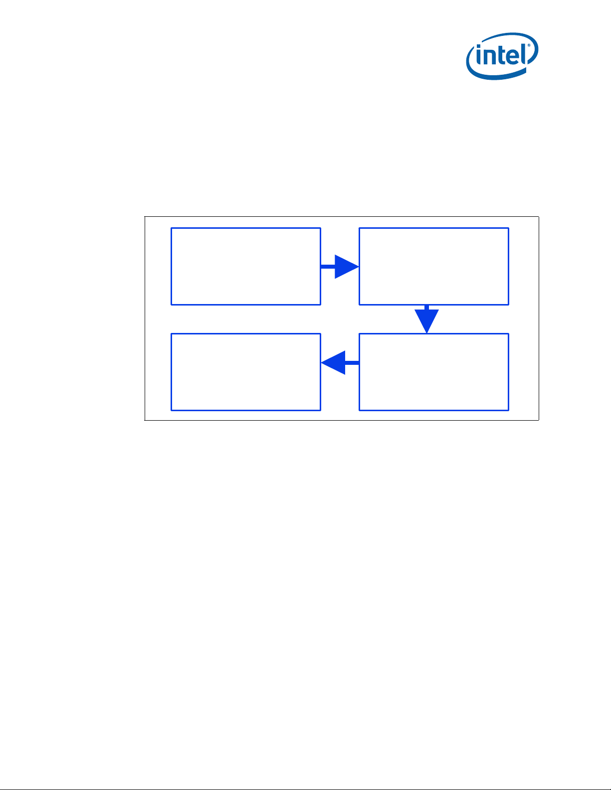
dependent. A simplified process flow of this methodology can be seen in Figure 5-2.
Figure 5-2. Flow Chart of Knowledge-Based Reliability Evaluation Methodology
August 2010 Thermal/Mechanical Design Guide
Order Number: 323107-002US 35
A detailed description of this methodology is at:
ftp://download.intel.com/technology/itj/q32000/pdf/reliability .pdf.
§
Intel® Xeon® Processor C5500/C3500 Series and LGA1366 Socket
Page 36

Thermal Specifications
6 Thermal Specifications
6.1 Package Thermal Specifications
The Intel® Xeon® processor C5500/C3500 series requires a thermal solution to
maintain temperatures within its operating limits. Any attempt to operate the processor
outside these operating limits may result in permanent damage to the processor and
potentially other components within the system. Maintaining the proper thermal
environment is key to reliable, long-term system operation.
A complete solution includes both component and system level thermal management
features. Component level thermal solutions can include active or passive heatsinks
attached to the processor integrated heat spreader (IHS).
This section provides data necessary for developing a complete thermal solution. For
more information on designing a component level thermal solution, see Section 7.
6.1.1 Thermal Specifications
To allow the optimal operation and long-term reliability of Intel processor-based
systems, the processor must remain within the minimum and maximum case
temperature (T
Thermal solutions not designed to provide this level of thermal capability may affect the
long-term reliability of the processor and system. These specifications are based on
pre-silicon estimates. These specifications may be further updated as more data
becomes available. Processors are listed here by TDP (Multiple SKUs may have the
same TDP and same spec).
®
The Intel
managing processor temperatures that is intended to support acoustic noise reduction
through fan speed control and to assure processor reliability. Selection of the
appropriate fan speed is based on the relative temperature data reported by the
processor’s Platform Environment Control Interface (PECI) as described in Section 6.3.
If PECI is less than TCONTROL, then the case temperature is permitted to exceed the
Thermal Profile, but PECI must remain at or below TCONTROL. If PECI >= TCONTROL,
then the case temperature must meet the Thermal Profile. The temperature reported
over PECI is always a negative value and represents a delta below the onset of thermal
control circuit (TCC) activation, as indicated by PROCHO T# (see Section 6.2, Processor
Thermal Features). Systems that implement fan speed control must be designed to use
this data. Systems that do not alter the fan speed only need to guarantee the case
temperature meets the thermal profile specifications.
The Intel
single Thermal Profile. See specifications below. For this processor, it is expected that
the Thermal Control Circuit (TCC) wo uld only be activ ated for very brief periods of time
when running the most power-intensive applications.
The Intel
single Thermal Profile. For this processor, it is expected that the Thermal Control Circuit
(TCC) would only be activated for very brief periods of time when running the most
power-intensive applications.
Xeon® processor C5500/C3500 series implements a methodology for
®
Xeon® processor EC5500 and EC3500 series (85 W and 65 W) supports a
®
Celeron® processor P1053 (30 W) (see specifications below) supports a
) specifications as defined by the applicable thermal profile.
CASE
August 2010 Thermal/Mechanical Design Guide
Order Number: 323107-002US 36
Intel® Xeon® Processor C5500/C3500 Series and LGA1366 Socket
Page 37
Thermal Specifications
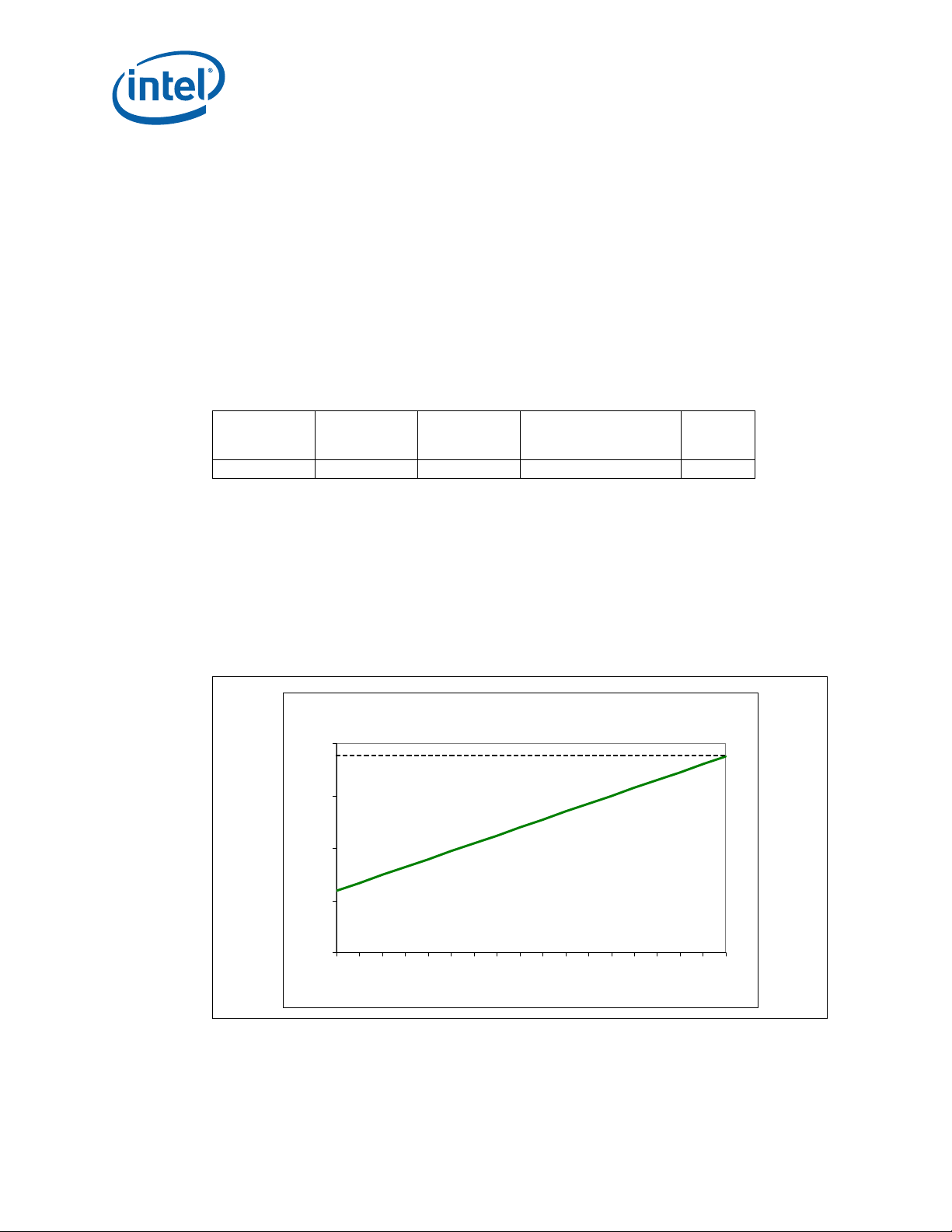
Thermal Profile
40
50
60
70
80
0 5 10 15 20 25 30 35 40 45 50 55 60 65 70 75 80 85
Power [W ]
Tcase [C]
Thermal Profile
Tc = 0.3 03* P + 51. 8
The Intel® Xeon® processor LC5500 and LC3500 series (60 W, 48 W, 35 W, and 23 W)
all support Thermal Profiles with nominal and short-term conditions designed to meet
NEBS Level 3 compliance. See specifications below. F or these SKUs, op eration at either
the nominal or short-term thermal profiles should result in virtually no TCC activation.
Analysis indicates that real applications are unlikely to cause the processor to consume
maximum power dissipation for sustained time periods. Intel recommends that
complete thermal solution designs target the Thermal Design Power (TDP), instead of
the maximum processor power consumption. The Adaptive Thermal Monitor feature is
intended to help protect the processor in the event that an application exceeds the TDP
recommendation for a sustained time period. For more details on this feature, see
Section 6.2. The Adaptive Thermal Monitor feature must be enabled for the
processor to remain within its specifications.
Table 6-1. Intel® Xeon® Processor EC5549 and EC5509 Thermal Specifications
Core
Frequency
Launch to FMB 85 5 See Figure 6-1; Table 6-2 1, 2, 3, 4, 5
Notes:
1. These values are specified at V
the processor is not to be subjected to any static V
specified ICC. See the loadline specifications in the Datasheet.
2. Thermal Design Power (TDP) should be used for processor thermal solution design targets. TDP is not the
maximum power that the processor can dissipate. TDP is measured at maximum T
3. These specifications are based on initial silicon characterization. These specifications may be further
updated as more characterization data becomes available.
4. Power specifications are defined at all VIDs found in the Datasheet. The Intel
C3500 series may be shipped under multiple VIDs for each frequency.
5. FMB (Flexible Motherboard) guidelines provide a design targ et for meeting all plan ned p roces sor fre quency
requirements.
Thermal Design
Power
(W)
Minimum
CASE
T
(°C)
for all processor frequencies. Systems must be designed to ensure
CC_MAX
CC
Maximum
CASE
T
(°C)
and ICC combination wherein VCC exceeds V
Notes
.
CASE
®
Xeon® processor C5500/
CC_MAX
at
Figure 6-1. Intel® Xeon® Processor EC5549 and EC5509 Thermal Profile
Notes:
1. Intel® Xeon® processor EC5549 and EC5509 Thermal Profile is representative of a volumetrically
unconstrained platform. See Table 6-2 for discrete points that constitute the thermal profile.
2. Implementation of Intel
TCC activation.
®
Xeon® processor EC5549 and EC5509 Thermal Profile should result in virtually no
®
Xeon® Processor C5500/C3500 Series and LGA1366 Socket
Intel
Thermal/Mechanical Design Guide August 2010
37 Order Number: 323107-002US
Page 38
Thermal Specifications
Table 6-2. Intel® Xeon® Processor EC5549 and EC5509 Thermal Profile
Power (W) T
CASE_MAX
(°C)
0 51.8
5 53.3
10 54.8
15 56.3
20 57.9
25 59.4
30 60.9
35 62.4
40 63.9
45 65.4
50 67.0
55 68.5
60 70.0
65 71.5
70 73.0
75 74.5
80 76.0
85 77.6
Table 6-3. Intel® Xeon® Processor EC3539 and EC5539 Thermal Specifications
Core
Frequency
Thermal Design
Power
(W)
Minimum
CASE
T
(°C)
Launch to FMB 65 5 See Figure 6-2; Table 6-4 1, 2, 3, 4, 5
Maximum
CASE
T
(°C)
Notes
Notes:
1. These values are specified at V
the processor is not to be subjected to an y static V
specified ICC. See the loadline specifications in the Datasheet.
2. Thermal Design Power (TDP) should be used for processor thermal solution design targets. TDP is not the
maximum power that the processor can dissipate. TDP is measured at maximum T
3. These specifications are based on initial silicon characterization. These specifications may be further
updated as more characterization data becomes available.
4. Power specifications are defined at all VIDs found in the Datasheet. The Intel
C3500 series Intel
frequency.
5. FMB (Flexible Motherboard) guidelines provide a design target for meeting all planned processor frequency
requirements.
August 2010 Thermal/Mechanical Design Guide
Order Number: 323107-002US 38
®
Xeon® processor C5500/C3500 series may be shipped under multiple VIDs for each
for all processor frequencies. Systems must be designed to ensure
CC_MAX
and ICC combination wherein VCC exceeds V
CC
.
CASE
®
Xeon® processor C5500/
Intel® Xeon® Processor C5500/C3500 Series and LGA1366 Socket
CC_MAX
at
Page 39
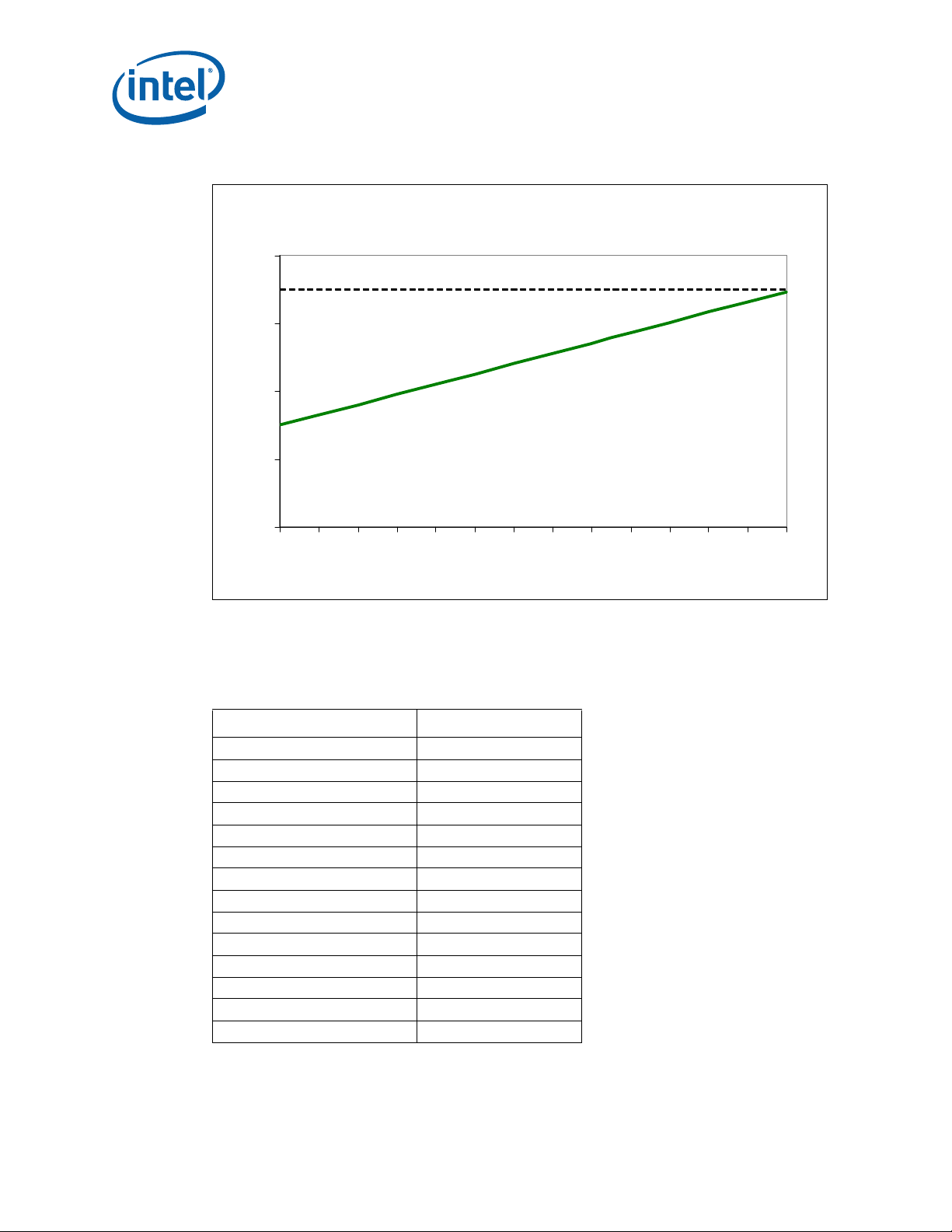
Figure 6-2. Intel® Xeon® Processor EC3539 and EC5539 Thermal Profile
Thermal Profile
40
50
60
70
80
0 5 10 15 20 25 30 35 40 45 50 55 60 65
Power [ W ]
Tcase [C]
Tc = 0. 30 2* P + 55
Thermal Profile
Thermal Specifications
Notes:
1. Intel® Xeon® processor EC3539 and EC5539 Thermal Profile is representative of a volumetrically
unconstrained platform. See Table 6-4 for discrete points that constitute the thermal profile.
2. Implementation of Intel
no TCC activation.
®
Xeon® processor EC3539 and EC5539 Thermal Profile should result in virtually
Table 6-4. Intel® Xeon® Processor EC3539 and EC5539 Thermal Profile
Power (W) T
0 55.0
5 56.5
10 58.0
15 59.5
20 61.0
25 62.6
30 64.1
35 65.6
40 67.1
45 68.6
50 70.1
55 71.6
60 73.1
65 74.6
CASE_MAX
(°C)
®
Xeon® Processor C5500/C3500 Series and LGA1366 Socket
Intel
Thermal/Mechanical Design Guide August 2010
39 Order Number: 323107-002US
Page 40
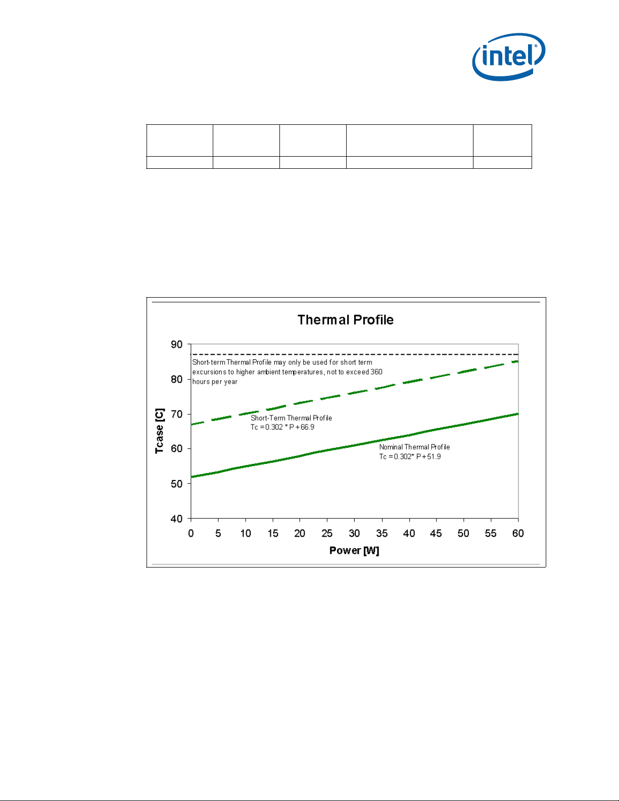
Thermal Specifications
Table 6-5. Intel® Xeon® Processor LC5528 Thermal Specifications
Core
Frequency
Thermal Design
Power
(W)
Minimum
CASE
T
(°C)
Launch to FMB 60 5 See Figure 6-3; Table 6-6 1, 2, 3, 4, 5
Notes:
1. These values are specified at V
the processor is not to be subjected to an y static V
specified ICC. See the loadline specifications in the Datasheet.
2. Thermal Design Power (TDP) should be used for processor thermal solution design targets. TDP is not the
maximum power that the processor can dissipate. TDP is measured at maximum T
3. These specifications are based on initial silicon characterization. These specifications may be further
updated as more characterization data becomes available.
4. Power specifications are defined at all VIDs found in the Datasheet. The Intel
C3500 series may be shipped under multiple VIDs for each frequency.
5. FMB (Flexible Motherboard) guidelines provide a design target for meeting all planned processor frequency
requirements.
for all processor frequencies. Systems must be designed to ensure
CC_MAX
and ICC combination wherein VCC exceeds V
CC
Maximum
T
CASE
(°C)
Figure 6-3. Intel® Xeon® Processor LC5528 Thermal Profile
Notes
CC_MAX
.
CASE
®
Xeon® processor C5500/
at
Notes:
1. Intel® Xeon® processor LC5528 Thermal Profile is representative of a volumetrically constrained platform.
See Table 6-7 for discrete points that constitute the thermal profile.
2. Implementation of Intel
in virtually no TCC activation. Furthermore, utilization of thermal solutions that do not meet this Thermal
Profile will result in increased probability of TCC activation and may incur measurable performance loss.
3. The Nominal Thermal Profile must be used for all normal operating conditions, or for products that do not
require NEBS Level 3 compliance.
4. The Short-Term T hermal Profile may only be used for short-term excursions to higher ambient operating
temperatures, not to exceed 360 hours per year, as compliant with NEBS Level 3. Operation at the ShortTerm Thermal Profile for durations exceeding 360 hours per year violate the processor thermal
®
Xeon® processor LC5528 nominal and short-term thermal profiles should result
specifications and may result in permanent damage to the processor.
August 2010 Thermal/Mechanical Design Guide
Order Number: 323107-002US 40
Intel® Xeon® Processor C5500/C3500 Series and LGA1366 Socket
Page 41
Table 6-6. Intel® Xeon® Processor LC5528 Thermal Profile
Thermal Specifications
Power (W) N ominal T
CASE_MAX
(°C)
Short-term T
0 51.9 66.9
5 53.4 68.4
10 54.9 69.9
15 56.4 71.4
20 57.9 72.9
25 59.5 74.5
30 61.0 76.0
25 62.5 77.5
40 64.0 79.0
45 65.5 80.5
50 67.0 82.0
55 68.5 83.5
60 70.0 85.0
Table 6-7. Intel® Xeon® Processor LC5518 Thermal Specifications
Core
Frequency
Thermal Design
Power
(W)
Minimum
CASE
T
(°C)
Launch to FMB 48 5 See Figure 6-4; Table 6-8 1, 2, 3, 4, 5
Notes:
1. These values are specified at V
the processor is not to be subjected to any static V
specified ICC. See the loadline specifications in the Datasheet.
2. Thermal Design Power (TDP) should be used for processor thermal solution design targets. TDP is not the
maximum power that the processor can dissipate. TDP is measured at maximum T
3. These specifications are based on initial silicon characterization. These specifications may be further
updated as more characterization data becomes available.
4. Power specifications are defined at all VIDs found in the Datasheet. The Intel
C3500 series may be shipped under multiple VIDs for each frequency.
5. FMB (Flexible Motherboard) guidelines provide a design targ et for meeting all plan ned p roces sor fre quency
requirements.
for all processor frequencies. Systems must be designed to ensure
CC_MAX
and ICC combination wherein VCC exceeds V
CC
Maximum
CASE
T
(°C)
(°C)
CASE_MAX
Notes
.
CASE
®
Xeon® processor C5500/
CC_MAX
at
®
Xeon® Processor C5500/C3500 Series and LGA1366 Socket
Intel
Thermal/Mechanical Design Guide August 2010
41 Order Number: 323107-002US
Page 42

Thermal Specifications
Figure 6-4. Intel® Xeon® Processor LC5518 Thermal Profile
Notes:
1. Intel® Xeon® processor LC5518 Thermal Profile is representative of a volumetrically constrained platform.
See Table 6-8 for discrete points that constitute the thermal profile.
2. Implementation of Intel
in virtually no TCC activation. Furthermore, utilization of thermal solutions that do not meet this Thermal
Profile will result in increased probability of TCC activation and may incur measurable performance loss.
3. The Nominal Thermal Profile must be used for all normal operating conditions, or for products that do not
require NEBS Level 3 compliance.
4. The Short-Term T hermal Profile may only be used for short-term excursions to higher ambient operating
temperatures, not to exceed 360 hours per year per year, as compliant with NEBS Level 3. Operation at the
Short-Term Thermal Profile for durations exceeding 360 hours per year violate the processor thermal
specifications and may result in permanent damage to the processor.
®
Xeon® processor LC5518 nominal and short-term thermal profiles should result
Table 6-8. Intel® Xeon® Processor LC5518 Thermal Profile
Power (W) Nominal T
CASE_MAX
0 52.0 67.0
5 54.7 69.7
10 57.3 72.3
15 60.0 75.0
20 62.6 77.6
25 65.3 80.3
30 68.0 83.0
35 70.6 85.6
40 73.3 88.3
48 77.5 92.5
(°C)
Short-term T
(°C)
CASE_MAX
August 2010 Thermal/Mechanical Design Guide
Order Number: 323107-002US 42
Intel® Xeon® Processor C5500/C3500 Series and LGA1366 Socket
Page 43

Table 6-9. Intel® Celeron® Processor P1053 Thermal Specifications
Thermal Profile
40
50
60
70
0 5 10 15 20 25 30
Power [ W]
Tcase [C]
Thermal Profile
Tc = 0.3 13* P + 55
Core
Frequency
Thermal Design
Power
(W)
Minimum
CASE
T
(°C)
Launch to FMB 30 5 See Figure 6-5; Table 6-10 1, 2, 3, 4, 5
Maximum
T
CASE
(°C)
Thermal Specifications
Notes
1. These values are specified at V
the processor is not to be subjected to any static V
specified ICC. See the loadline specifications in the Datasheet.
2. Thermal Design Power (TDP) should be used for processor thermal solution design targets. TDP is not the
maximum power that the processor can dissipate. TDP is measured at maximum T
3. These specifications are based on initial silicon characterization. These specifications may be further
updated as more characterization data becomes available.
4. Power specifications are defined at all VIDs found in the Datasheet. The Intel
C3500 series may be shipped under multiple VIDs for each frequency.
5. FMB (Flexible Motherboard) guidelines provide a design targ et for meeting all plan ned p roces sor fre quency
requirements.
for all processor frequencies. Systems must be designed to ensure
CC_MAX
and ICC combination wherein VCC exceeds V
CC
Figure 6-5. Intel® Celeron® Processor P1053 Thermal Profile
CC_MAX
.
CASE
®
Xeon® processor C5500/
at
Notes:
1. Intel® Celeron® processor P1053 Thermal Profile is representative of a volumetrically unconstrained
platform. See Table 6-12 for discrete points that constitute the thermal profile.
2. Implementation of Intel
activation.
Table 6-10. Intel® Celeron® Processor P1053 Thermal Profile
Power (W) T
0 55.0
®
Xeon® Processor C5500/C3500 Series and LGA1366 Socket
Intel
Thermal/Mechanical Design Guide August 2010
43 Order Number: 323107-002US
5 56.6
10 58.1
15 59.7
20 61.3
25 62.8
30 64.4
®
Celeron® processor P1053 Thermal Profile should result in virtually no TCC
CASE_MAX
(°C)
Page 44

Therma l Pro file
40
50
60
70
80
90
100
0 5 10 15 20 25 30 35
Power [W ]
Tcase [C]
Short-Term Thermal Profile
Tc = 0. 970 * P + 60
Nominal Thermal Profile
Tc = 0. 970 * P + 45
Short-term Thermal P rofil e m ay only be used for
short term ex curs i ons to higher ambient
temperatures, not to ex ceed 360 hours per y ear
Thermal Specifications
Table 6-11. Intel® Xeon® Processor LC3528 Thermal Specifications
Core
Frequency
Launch to FMB 35 5 See Figure 6-6; Table 6-12 1, 2, 3, 4, 5
Notes:
1. These values are specified at V
the processor is not to be subjected to an y static V
specified ICC. See the loadline specifications in the Datasheet.
2. Thermal Design Power (TDP) should be used for processor thermal solution design targets. TDP is not the
maximum power that the processor can dissipate. TDP is measured at maximum T
3. These specifications are based on initial silicon characterization. These specifications may be further
updated as more characterization data becomes available.
4. Power specifications are defined at all VIDs found in the Datasheet. The Intel
C3500 series may be shipped under multiple VIDs for each frequency.
5. FMB (Flexible Motherboard) guidelines provide a design target for meeting all planned processor frequency
requirements.
Thermal Design
Power
(W)
Minimum
CASE
T
(°C)
for all processor frequencies. Systems must be designed to ensure
CC_MAX
and ICC combination wherein VCC exceeds V
CC
Maximum
T
CASE
(°C)
Figure 6-6. Intel® Xeon® Processor LC3528 Thermal Profile
Notes
CC_MAX
.
CASE
®
Xeon® processor C5500/
at
Notes:
1. Intel® Xeon® processor LC3528 Thermal Profile is representative of a volumetrically constrained platform.
See Table 6-12 for discrete points that constitute the thermal profile.
2. Implementation of Intel
in virtually no TCC activation. Furthermore, utilization of thermal solutions that do not meet this Thermal
Profile will result in increased probability of TCC activation and may incur measurable performance loss.
3. The Nominal Thermal Profile must be used for all normal operating conditions, or for products that do not
require NEBS Level 3 compliance.
4. The Short-Term T hermal Profile may only be used for short-term excursions to higher ambient operating
temperatures, not to exceed 96 hours per instance, 360 hours per year, and a maximum of 15 instances
per year, as compliant with NEBS Level 3. Operation at the Short-Term Thermal Profile for durations
exceeding 360 hours per year violate the processor thermal specifications and may result in permanent
damage to the processor.
®
Xeon® processor LC3528 nominal and short-term thermal profiles should result
Intel® Xeon® Processor C5500/C3500 Series and LGA1366 Socket
August 2010 Thermal/Mechanical Design Guide
Order Number: 323107-002US 44
Page 45

Table 6-12. Intel® Xeon® Processor LC3528 Thermal Profile
Thermal Specifications
Power (W) N ominal T
CASE_MAX
(°C)
Short-term T
0 45.0 60.0
5 49.9 64.9
10 54.7 69.7
15 59.6 74.6
20 64.4 79.4
25 69.3 84.3
30 74.1 89.1
35 79.0 94.0
Table 6-13. Intel® Xeon® Processor LC3518 Thermal Specifications
Core
Frequency
Thermal Design
Power
(W)
Minimum
CASE
T
(°C)
Launch to FMB 23 5 See Figure 6-7; Table 6-14 1, 2, 3, 4, 5
Notes:
1. These values are specified at V
the processor is not to be subjected to any static V
specified ICC. See the loadline specifications in the Datasheet.
2. Thermal Design Power (TDP) should be used for processor thermal solution design targets. TDP is not the
maximum power that the processor can dissipate. TDP is measured at maximum T
3. These specifications are based on initial silicon characterization. These specifications may be further
updated as more characterization data becomes available.
4. Power specifications are defined at all VIDs found in the Datasheet. The Intel
C3500 series may be shipped under multiple VIDs for each frequency.
5. FMB (Flexible Motherboard) guidelines provide a design targ et for meeting all plan ned p roces sor fre quency
requirements.
for all processor frequencies. Systems must be designed to ensure
CC_MAX
and ICC combination wherein VCC exceeds V
CC
Maximum
T
CASE
(°C)
(°C)
CASE_MAX
Notes
.
CASE
®
Xeon® processor C5500/
CC_MAX
at
®
Xeon® Processor C5500/C3500 Series and LGA1366 Socket
Intel
Thermal/Mechanical Design Guide August 2010
45 Order Number: 323107-002US
Page 46

Thermal Profile
40
50
60
70
80
90
100
0 5 10 15 20
Power [ W ]
Tcase [C]
Tc = 1.50 * P + 60
Nominal Thermal P rofil e
Tc = 1.50 * P + 45
Short-t erm Thermal Profile m ay onl y be us ed for
short term ex curs i ons to higher ambient
tem peratures , no t to ex ceed 360 hours per y ear
23
Thermal Specifications
Figure 6-7. Intel® Xeon® Processor LC3518 Thermal Profile
Short -Term Thermal P rofil e
Notes:
1. Intel® Xeon® processor LC3518 Thermal Profile is representative of a volumetrically constrained platform.
2. Implementation of Intel
3. The Nominal Thermal Profile must be used for all normal operating conditions, or for products that do not
4. The Short-Term T hermal Profile may only be used for short-term excursions to higher ambient operating
Table 6-14. Intel® Xeon® Processor LC3518 Thermal Profile
See Table 6-14 for discrete points that constitute the thermal profile.
in virtually no TCC activation. Furthermore, utilization of thermal solutions that do not meet this Thermal
Profile will result in increased probability of TCC activation and may incur measurable performance loss.
require NEBS Level 3 compliance.
temperatures, not to exceed 96 hours per instance, 360 hours per year, and a maximum of 15 instances
per year, as compliant with NEBS Level 3. Operation at the Short-Term Thermal Profile for durations
exceeding 360 hours per year violate the processor thermal specifications and may result in permanent
damage to the processor.
Power (W) Nominal T
0 45.0 60.0
5 52.5 67.5
10 60.0 75.0
15 67.5 82.5
20 75.0 90.0
23 79.5 94.5
®
Xeon® processor LC3518 nominal and short-term thermal profiles should result
CASE_MAX
(°C)
Short-term T
(°C)
CASE_MAX
August 2010 Thermal/Mechanical Design Guide
Order Number: 323107-002US 46
Intel® Xeon® Processor C5500/C3500 Series and LGA1366 Socket
Page 47

6.1.2 Thermal Metrology
Notes:
1. Figure is not to scale and is for reference only.
2. B1: Max = 45.07 mm, Min = 44.93 mm.
3. B2: Max = 42.57 mm, Min = 42.43 mm.
4. C1: Max = 39.1 mm, Min = 38.9 mm.
5. C2: Max = 36.6 mm, Min = 36.4 mm.
6. C3: Max = 2.3 mm, Min = 2.2 mm
7. C4: Max = 2.3 mm, Min = 2.2 mm.
Thermal Specifications
The minimum and maximum case temperatures (T
Profiles above and are measured at the geometric top center of the T TV integrated heat
spreader (IHS). Figure 6-8 illustrates the location where T
measurements should be made.
Figure 6-8. TTV Case Temperature (T
) Measurement Location
CASE
) are specified in Thermal
CASE
temperature
CASE
®
Xeon® Processor C5500/C3500 Series and LGA1366 Socket
Intel
Thermal/Mechanical Design Guide August 2010
47 Order Number: 323107-002US
Page 48

Thermal Specifications
6.2 Processor Thermal Features
6.2.1 Processor Temperature
A new feature in the Intel® Xeon® processor C5500/C3500 series is a software
readable field in the IA32_TEMPERATURE_TARGET register that contains the minimum
temperature at which the TCC will be activated and PROCHOT# will be asserted. The
TCC activation temperature is calibrated on a part-by-part basis and normal factory
variation may result in the actual TCC activation temperature being higher than the
value listed in the register. TCC activation temperatures may change based on
processor stepping, frequency or manufacturing efficiencies.
Note: There is no specified correlation between DTS temperatures and processor case
temperatures; therefore it is not possible to use this feature to ensure the processor
case temperature meets the Thermal Profile specifications.
6.2.2 Adaptive Thermal Monitor
The Adaptive Thermal Monitor feature provides an enhanced method for controlling the
processor temperature when the processor silicon reaches its maximum operating
temperature. Adaptive Thermal Monitor uses Thermal Control Circuit (TCC) activation
to reduce processor power via a combination of methods. The first method (Frequency/
VID control) involves the processor adjusting its operating frequency (via the core ratio
multiplier) and input voltage (via the VID signals). This combination of reduced
frequency and VID results in a reduction to the processor power consumption. The
second method (clock modulation) reduces power consumption by modulating (starting
and stopping) the internal processor core clocks. The processor intelligently selects the
appropriate TCC method to use on a dynamic basis. BIOS is not required to select a
specific method (as with previous-generation processors supporting TM1 or TM2).
The Adaptive Thermal Monitor feature must be enabled for th e processor to be
operating within specifications. The temperature at which Adaptive Thermal
Monitor activates the Thermal Control Circuit is not user configurable and is not
software visible. Snooping and interrupt processing are performed in the normal
manner while the TCC is active.
With a properly designed and characterized thermal solution, it is anticipated that the
TCC would only be activated for very short periods of time when running the most
power intensive applications. The processor performance impact due to these brief
periods of TCC activation is expected to be so minor that it would be immeasurable. An
under-designed thermal solution that is not able to prevent excessive activation of the
TCC in the anticipated ambient environment ma y cause a noticeable performance loss,
and in some cases may result in a T
that exceeds the specified maximum
CASE
temperature and may affect the long-term reliability of the processor. In addition, a
thermal solution that is significantly under-designed may not be capable of cooling the
processor even when the TCC is active continuously.
The duty cycle for the TCC, when activated by the Thermal Monitor, is factory
configured and cannot be modified. The Thermal Monitor does not require any
additional hardware, software drivers, or interrupt handling routines.
The following sections provide more details on the different TCC mechanisms used by
the Intel
®
Xeon® processor C5500/C3500 series.
August 2010 Thermal/Mechanical Design Guide
Order Number: 323107-002US 48
Intel® Xeon® Processor C5500/C3500 Series and LGA1366 Socket
Page 49
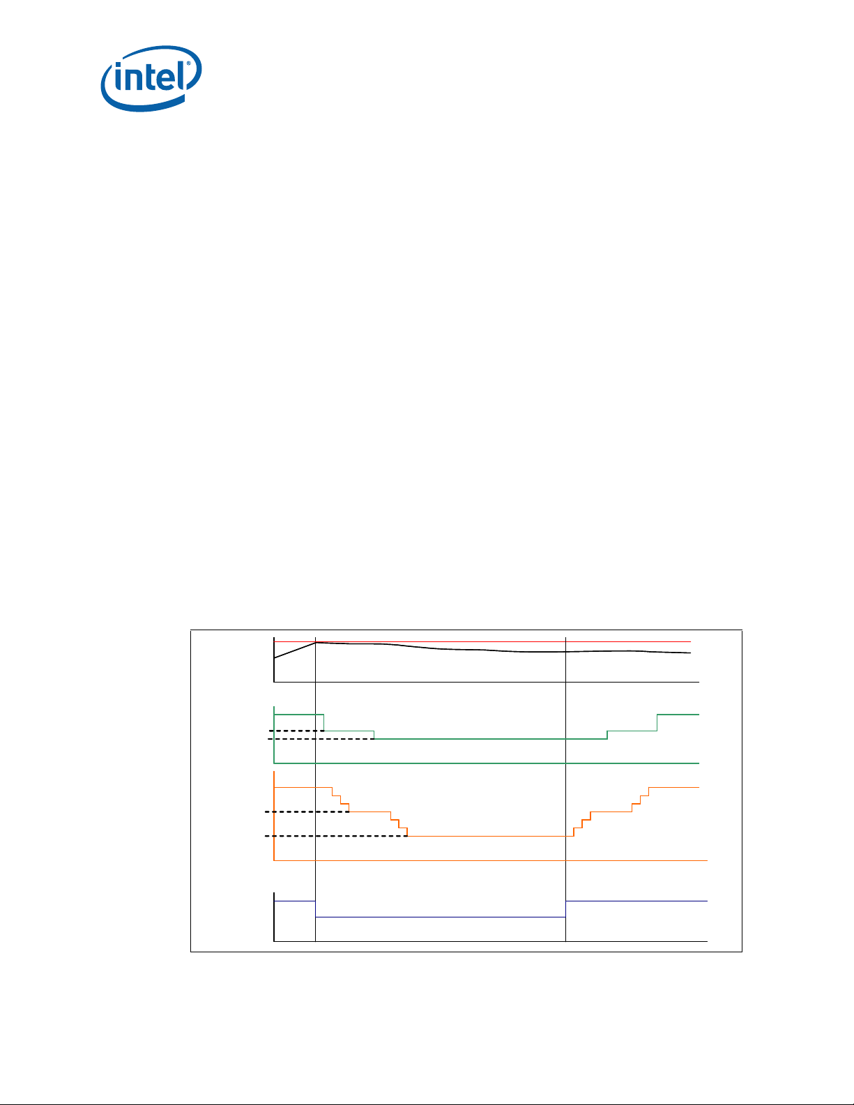
6.2.2.1 Frequency/VID Control
Temperatu re
f
MAX
f
1
f
2
VIDf
MAX
VID
Frequency
VIDf
2
VIDf
1
PROCHOT#
Temperatu re
f
MAX
f
1
f
2
VIDf
MAX
VID
Frequency
VIDf
2
VIDf
1
PROCHOT#
The processor uses Frequency/VID control whereby TCC activation causes the
processor to adjust its operating frequency (via the core ratio multiplier) and input
voltage (via the VID signals). This combination of reduced frequency and VID results in
a reduction to the processor power consumption.
This method includes multiple operating points, each consisting of a specific operating
frequency and voltage. The first operating point represents the normal operating
condition for the processor. The remaining points consist of both lower operating
frequencies and voltages. When the TCC is activated, the processor automatically
transitions to the new operating frequency. This transition occurs very rapidly (on the
order of 2 microseconds).
Once the new operating frequency is engaged, the processor will transition to the new
core operating voltage by issuing a new VID code to the voltage regulator. The voltage
regulator must support dynamic VID steps to support this method. During the voltage
change, it will be necessary to transition through multiple VID codes to reach the target
operating voltage. Each step will be one VID table entry (see the Intel
Processor C5500/C3500 Series Datsheet). The processor continues to execute
instructions during the voltage transition. Operation at the lower voltages reduces the
power consumption of the processor.
Thermal Specifications
®
Xeon®
A small amount of hysteresis has been included to prevent rapid active/inactive
transitions of the TCC when the processor temperature is near its maximum operating
temperature. Once the temperature has dropped below the maximum operating
temperature, and the hysteresis timer has expired, the operating frequency and
voltage transition back to the normal system operating point via the intermediate VID/
frequency points. Transition of the VID code will occur first, to insure proper operation
once the processor reaches its normal operating frequency. Refer to Figure 6-9 for an
illustration of this ordering.
Figure 6-9. Frequency and Voltage Ordering
®
Xeon® Processor C5500/C3500 Series and LGA1366 Socket
Intel
Thermal/Mechanical Design Guide August 2010
49 Order Number: 323107-002US
Page 50

Thermal Specifications
6.2.2.2 Clock Modulation
Clock modulation is performed by alternately turning the clocks off and on at a duty
cycle specific to the processor (factory configured to 37.5% on and 62.5% off). The
period of the duty cycle is configured to 32 microseconds when the TCC is active. Cycle
times are independent of processor frequency. A small amount of hysteresis has been
included to prevent rapid active/inactive transitions of the TCC when the processor
temperature is near its maximum operating temperature. Once the temperature has
dropped below the maximum operating temperature, and the hysteresis timer has
expired, the TCC goes inactive and clock modulation ceases. Clock modulation is
automatically engaged as part of the TCC activation when the Frequency/VID targets
are at their minimum settings. It may also be initiated by software at a configurable
duty cycle.
6.2.2.3 On-Demand Mode
The processor provides an auxiliary mechanism that allows system software to force
the processor to reduce its power consumption. This mechanism is referred to as “OnDemand” mode and is distinct from the Adaptive Thermal Monitor feature. On-Demand
mode is intended as a means to reduce system level power consumption. Systems
utilizing the Intel
this mechanism to limit the processor temperature. If bit 4 of the
IA32_CLOCK_MODULATION MSR is set to a ‘1’, the processor will immediately reduce
its power consumption via modulation (starting and stopping) of the internal core clock,
independent of the processor temperature. When using On-Demand mode, the duty
cycle of the clock modulation is programmable via bits 3:1 of the same
IA32_CLOCK_MODULATION MSR. In On-Demand mode, the duty cycle can be
programmed from 12.5% on/ 87.5% off to 87.5% on/12.5% off in 12.5% increments.
On-Demand mode may be used in conjunction with the Adaptive Thermal Monitor;
however, if the system tries to enable On-Demand mode at the same time the TCC is
engaged, the factory configured duty cycle of the TCC will override the duty cycle
selected by the On-Demand mode.
®
Xeon® Processor 5500 Series must not rely on software usage of
6.2.2.4 PROCHOT# Signal
An external signal, PROCHOT# (processor hot), is asserted when the processor core
temperature has reached its maximum operating temperature. If Adaptive Thermal
Monitor is enabled (it must be enabled for the processor to be operating within
specification), the TCC will be active when PROCHOT# is asserted. The processor can
be configured to generate an interrupt upon the assertion or de-assertion of
PROCHOT#.
The PROCHOT# signal is bi-directional in that it can either signal when the processor
(any core) has reached its maximum operating temperature or be driven from an
external source to activate the TCC. The ability to activate the TCC via PROCHOT# can
provide a means for thermal protection of system components.
As an output, PROCHOT# will go active when the processor temperature monitoring
sensor detects that one or more cores has reached its maximum safe operating
temperature. This indicates that the processor Thermal Control Circuit (TCC) has been
activated, if enabled. As an input, assertion of PROCHOT# by the system will activate
the TCC for all cores. TCC activation when PROCHOT# is asserted by the system will
result in the processor immediately transitioning to the minimum frequency and
corresponding voltage (using Freq/VID control). Clock modulation is not activated in
this case. The TCC will remain active until the system de-asserts PROCHOT#.
August 2010 Thermal/Mechanical Design Guide
Order Number: 323107-002US 50
Intel® Xeon® Processor C5500/C3500 Series and LGA1366 Socket
Page 51

PROCHOT# can allow VR thermal designs to target maximum sustained current instead
of maximum current. Systems should still provide proper cooling for the VR, and rely
on PROCHOT# only as a backup in case of system cooling failure. The system thermal
design should allow the power delivery circuitry to operate within its temperature
specification even while the processor is operating at its Thermal Design Power.
With a properly designed and characterized thermal solution, it is anticipated that
PROCHOT# will only be asserted for very short periods of time when running the most
power intensive applications. An under-designed thermal solution that is not able to
prevent excessive assertion of PROCHOT# in the anticipated ambient environment may
cause a noticeable performance loss. Refer to the appropriate platform design guide
and for details on implementing the bi-directional PROCHOT# feature.
6.2.3 THERMTRIP# Signal
Regardless of whether or not Adaptive Thermal Monitor is enabled, in the event of a
catastrophic cooling failure, the processor will automatically shut down when the silicon
has reached an elevated temperature (see the THERMTRIP# definition in the
Datasheet). At this point, the THERMTRIP# signal will go active and stay active as
described in the Datasheet. THERMTRIP# activation is independent of processor
activity. If THERMTRIP# is asserted, processor core voltage (V
within the timeframe defined in the Datasheet. The temperature at which THERMTRIP#
asserts is not user configurable and is not software visible.
Thermal Specifications
) must be removed
CC
6.3 Platform Environment Control Interface (PECI)
6.3.1 Introduction
The Platform Environment Control Interface (PECI) is a one-wire interface that provides
a communication channel between Intel processor and chipset components to external
monitoring devices. The processor implements a PECI interface to allow communication
of processor thermal and other information to other devices on the platform. The
processor provides a digital thermal sensor (DTS) on each core for fan speed control.
The DTS is calibrated at the factory to provide a digital representation of processor
temperature relative PROCHOT# assertion. Instantaneous temperature readings from
the DTS are available via the IA32_TEMP_STATUS MSR; averaged DTS values are read
via the PECI interface.
The PECI physical layer is a self-clocked one-wire bus that begins each bit with a
driven, rising edge from an idle level near zero volts. The duration of the signal driven
high depends on whether the bit value is a logic '0' or logic '1'. PECI also includes
variable data transfer rate established with every message. The single wire interface
provides low board routing overhead for the multiple load connections in the congested
routing area near the processor and chipset components. Bus speed, error checking,
and low protocol overhead provides adequate link bandwidth and reliability to transfer
critical device operating conditions and configuration information.
6.3.1.1 Fan Speed Control with Digital Thermal Sensor
Fan speed control solutions use a value stored in the static v ariable, T
CONTROL
temperature data which is delivered over PECI (in response to a GetTemp0()
command) is compared to this T
CONTROL
reference. The DTS temperature is reported as
a relative value versus an absolute value. The temperature reported over PECI is
. The DTS
®
Xeon® Processor C5500/C3500 Series and LGA1366 Socket
Intel
Thermal/Mechanical Design Guide August 2010
51 Order Number: 323107-002US
Page 52

Thermal Specifications
always a negative value and represents a delta below the onset of thermal control
circuit (TCC) activation, as indicated by PROCHOT#. Therefore, as the temperature
approaches TCC activation, the value approaches zero degrees.
6.3.1.2 Processor Thermal Data Sample Rate and Filtering
The processor digital thermal sensor (DTS) provides an improved capability to monitor
device hot spots, which inherently leads to more varying temperature readings over
short time intervals. To reduce the sample rate requirements on PECI and improve
thermal data stability vs. time the processor DTS implements an averaging algorithm
that filters the incoming data. This filter is expressed mathematically as:
PECI(t) = PECI(t-1)+1/(2^X)*[Temp - PECI(t-1)]
Where: PECI(t) is the new averaged temperature, PECI(t-1) is the previous averaged
temperature Temp is the raw temperature data from the DTS, X is the Thermal
Averaging Constant (TAC).
Note: Only values read via the PECI interface are averaged. Temperature values read via the
IA32_TEMP_STATUS MSR are not averaged.
The Thermal Averaging Constant is a BIOS configurable value that determines the time
in milliseconds over which the DTS temperature values are averaged. Short averaging
times will make the averaged temperature values respond more quickly to DTS
changes. Long averaging times will result in better overall thermal smoothing but also
incur a larger time lag between fast DST temperature changes and the value read via
PECI.
Within the processor, the DTS converts an analog signal into a digital value
representing the temperature relative to TCC activation. The conversions are in
integers with each single number change corresponding to approximately 1° C. DTS
values reported via the internal processor MSR will be in whole integers.
As a result of the averaging function described above, DTS values reported over PECI
will include a 6-bit fractional value. Under typical operating conditions, where the
temperature is close to Tcontrol, the fractional values may not be of interest. But when
the temperature approaches zero, the fractional values can be used to detect the
activation of the TCC. An averaged temperature value between 0 and 1 can only occur
if the TCC has been activated during the averaging window. As TCC activation time
increases, the fractional value will approach zero. Fan control circuits can detect this
situation and take appropriate action as determined by the system designers. Of
course, fan control chips can also monitor the Prochot pin to detect TCC activ ation via a
dedicated input pin on the package.
August 2010 Thermal/Mechanical Design Guide
Order Number: 323107-002US 52
Intel® Xeon® Processor C5500/C3500 Series and LGA1366 Socket
Page 53

6.3.2 PECI Specifications
6.3.2.1 PECI Device Address
The processor PECI_ID# signal is used to configure the PECI address for the given
processor. The PECI register resides at:
• Address 30h when PECI_ID# is pulled to Vtt.
• Address 31h when PECI_ID# is terminated to ground.
6.3.2.2 PECI Command Support
PECI commands are in the Intel® Xeon® Processor C5500/C3500 Series Datasheet).
6.3.2.3 PECI Fault Handling Requirements
PECI is largely a fault tolerant interface, including noise immunity and error checking
improvements over other comparable industry standard interfaces. The PECI client is
as reliable as the device that it is embedded in, and thus given operating conditions
that fall under the specification, the PECI will always respond to requests and the
protocol itself can be relied upon to detect any transmission failures. There are,
however, certain scenarios in which the PECI is know to be unresponsive. Before a
power on RESET# and during RESET# assertion, PECI is not ensured to provide reliable
thermal data. System designs should implement a default power-on condition that
ensures proper processor operation during the time frame when reliable data is not
available via PECI.
Thermal Specifications
To protect platforms from potential operational or safety issues due to an abnormal
condition on PECI, the Host controller should take action to protect the system from
possible damaging states. If the Host controller cannot complete a valid PECI
transactions of GetTemp0() with a given PECI device over three consecutive failed
transactions or a one second max specified interval, then it should take appropriate
actions to protect the corresponding device and/or other system components from
overheating. The host controller may also implement an alert to software in the event
of a critical or continuous fault condition.
6.3.2.4 PECI GetTemp0() Error Code Support
The error codes supported for the processor GetTemp() command are listed in
Table 6-15.
Table 6-15. GetTemp0() Error Codes
Error Code Description
8000h General sensor error
§
®
Xeon® Processor C5500/C3500 Series and LGA1366 Socket
Intel
Thermal/Mechanical Design Guide August 2010
53 Order Number: 323107-002US
Page 54
Thermal Solutions
7 Thermal Solutions
This section describes 1U and ATCA reference heatsinks. These heatsink designs target
the Intel® Xeon® processor C5500/C3500 series and thermal design guidelines for the
processor.
7.1 Performance Targets
Table 7-1 provides boundary conditions and performance targets for 1U and ATCA
heatsinks. These values are used to generate processor thermal specifications and to
provide guidance for heatsink design. Other Intel
thermal solutions may work with the same retention. See the Intel® Xeon® Processor
5500 Series Thermal/Mechanical Design Guide.
Note: Custom heatsinks and high airflow AT CA designs can cool higher power processors than
typical ATCA.
Table 7-1. Boundary Conditions and Performance Targets
®
Xeon® Processor 5500 Series
Parameter Value
Altitude, system
ambient temp
TDP 85 W 65 W 30 W 60 W 48 W 35 W
1,4
T
LA
2
Ψ
CA
System form
3
factor
Heatsink
volumetric
Heatsink
technology
Note:
1. Local ambient temperature of the air entering the heatsink.
2. Max target (mean + 3σ) for thermal characterization parameter (Section 7.5.1).
3. Reference system configuration. Processors are not limited to these form factors.
4. Local Ambient Temperature written 45/60oC means 45oC under Nominal conditions but 60oC is allowed for
Short-Term NEBS excursions.
5. Passive heatsinks with TIM.
52 oC55
0.303o C/W 0.302o C/W 0.313o C/W 0.302o C/W 0.532o C/W 0.970o C/W
1U 1U 1U 1U or ATCA ATCA ATCA or
5
o
C55
90 x 90 x 27 mm (1U) 1U or Custom
Cu base, Al fins Cu base, Cu fins
Sea level, 40
o
C52/67
o
C
o
C 52/67o C45/60
ATCA
90 x 90 x 13 mm90 x 90 x 13
o
C
Dense Blade
mm
August 2010 Thermal/Mechanical Design Guide
Order Number: 323107-002US 54
Intel® Xeon® Processor C5500/C3500 Series and LGA1366 Socket
Page 55

For a 1U reference heatsink, see Appendix B for detailed drawings. Table 7-1 specifies
0.15
0.20
0.25
0.30
0.35
0.40
0.45
0.50
0 1020304050
CFM Through Fins
Ψ
ca, C/W
0.00
0.20
0.40
0.60
0.80
1.00
1.20
1.40
Δ
P, inch water
Mean
Ψ
ca
= 0.1430 + 1.141*CFM
-0.817
Ψ
ca
= 0.1430 + 1.141*CFM
-0.817
σ
= 0.0016 C/W
Δ
P = 1.9e-04CFM
2
+ 2.0e-02CFM
2
+ 2.0e-02CFM
Ψ
target at 11 CFM through the fins. Figure 7-1 shows ΨCA and pressure drop for the
CA
1U heatsink versus the airflow provided. Best-fit equations are provided to prevent
errors associated with reading the graph.
Figure 7-1. 1U Heatsink Performance Curves
Thermal Solutions
Intel
Thermal/Mechanical Design Guide August 2010
55 Order Number: 323107-002US
®
Xeon® Processor C5500/C3500 Series and LGA1366 Socket
Page 56
0
0.5
1
1.5
2
2.5
0 5 10 15 20 25 30 35
CFM Through Fins
Ψ
ca, C/W
0
0.4
0.8
1.2
1.6
2
Δ
P, inch water
Mean
Ψ
ca
= 0. 337 + 1.625 * CFM
-0.939
Thermal Solutions
For the ATCA reference heatsink, see Appendix B for detailed drawings. Table 7-1
specifies ΨCA target at 30 CFM per blade. Figure 7-2 shows ΨCA and pressure drop for
the ATCA heatsink versus the airflow provided. Best-fit equations are provided to
prevent errors associated with reading the graph.
Figure 7-2. ATCA Heatsink Performance Curves
P = 1. 3 e-04 CFM ^2 +1.1e-02 CFM
Δ
7.2 Heat Pipe Considerations
Figure 7-3 shows the orientation and position of the TTV die. The TTV die is sized and
positioned similar to the processor die.
August 2010 Thermal/Mechanical Design Guide
Order Number: 323107-002US 56
Intel® Xeon® Processor C5500/C3500 Series and LGA1366 Socket
Page 57
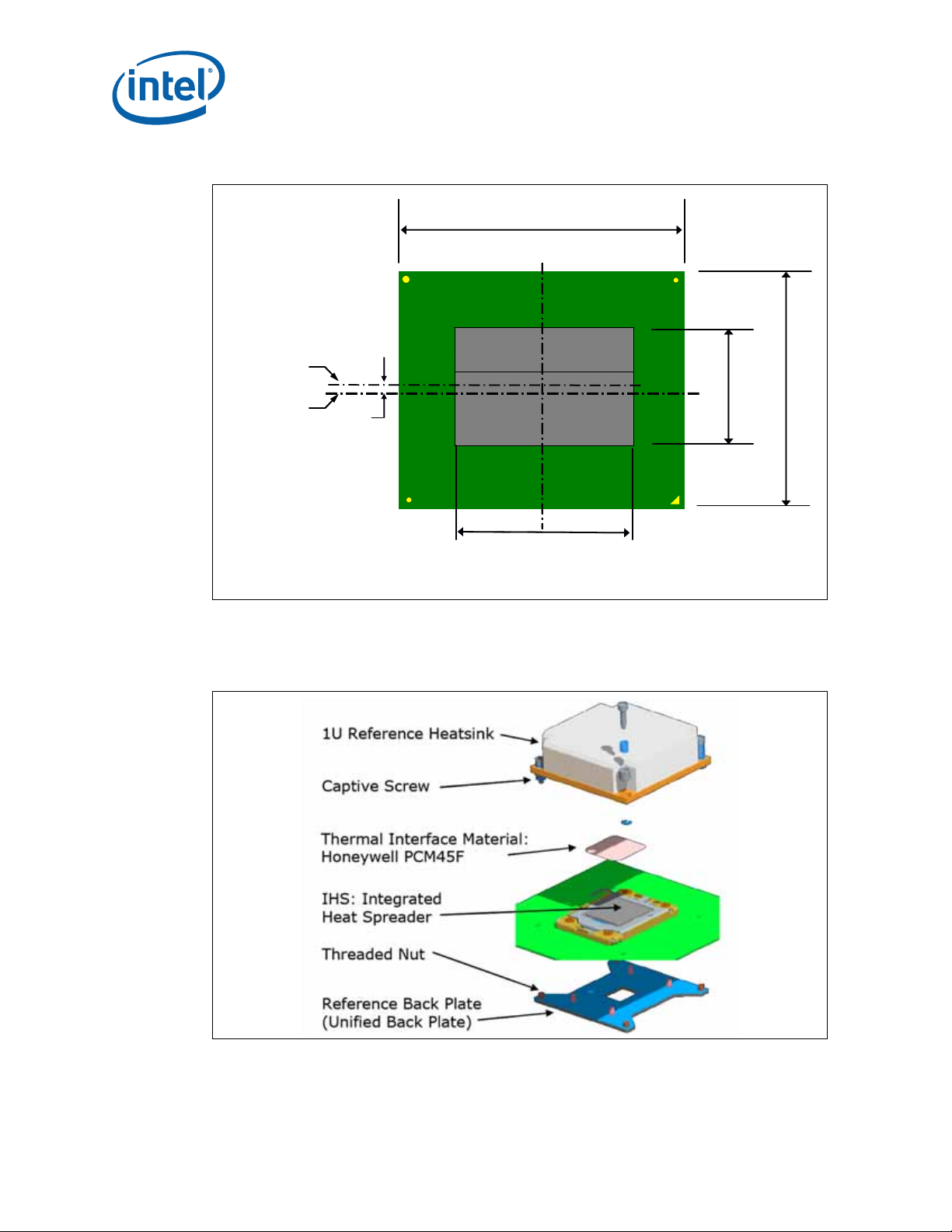
Figure 7-3. TTV Die Size and Orientation
Figure 1 - Side Views of Package with IHS (not to scale)
Core 1
Core 2
Core 3
Core 4
Cache Cache C ache Cach e
Uncore
Core
Cache
42.5
45
19.3
13.2
1.0
Package CL
Die CL
NOT TO SCALE
All Dimensions in mm
Thermal Solutions
7.3 Assembly
Figure 7-4. 1U Reference Heatsink Assembly
®
Xeon® Processor C5500/C3500 Series and LGA1366 Socket
Intel
Thermal/Mechanical Design Guide August 2010
57 Order Number: 323107-002US
Page 58

Thermal Solutions
The assembly process for the 1U reference heatsink begins with application of
Honeywell* PCM45F thermal interface material to improve conduction from the IHS.
Tape and roll format is recommended. Pad size is 35 x 35mm.
Next, the heatsink is positioned such that the heatsink fins are parallel to system
airflow. While lowering the heatsink onto the IHS, the four captive screws of the
heatsink are aligned to the four threaded nuts of the back plate.
Using a #2 Phillips driver, torque the four captive screws to 8 inch-pounds.
This assembly process is designed to produce a static load of 39 - 51 lbf, for 0.062" -
0.100" board thickness respectively. Honeywell PCM45F is expected to meet the
performance targets in Table 7-1 from 30 - 60 lbf. From Table 5-3, the Heatsink Static
Compressive Load of 0 - 60 lbf allows for designs that v ary from the 1U reference
heatsink. Example: A customer’s unique heatsink with very little static load (as little as
0 lbf) is acceptable from a socket loading perspective as long as the T
is met.
Compliance to board keepout zones in Appendix B is assumed for this assembly
process.
7.3.1 Thermal Interface Material (TIM)
specification
CASE
TIM should be verified to be within its recommended shelf life before use. Surfaces
should be free of foreign materials prior to application of TIM. Use isopropyl alcohol and
a lint-free cloth to remove old TIM before applying new TIM.
7.4 Structural Considerations
The mass of the 1U and ATCA reference heatsinks does not exceed 500 gm.
From Table 5-3, the Dynamic Compressive Load of 200 lbf max allows for designs that
exceed 500 gm as long as the mathematical product does not exceed 200 lbf. Example:
A heatsink of 2lb mass (908 gm) x 50 g (acceleration) x 2.0 Dynamic Amplification
Factor = 200 lbf. The Total Static Compressive Load (Table 5-3) should also be
considered in dynamic assessments.
The heatsink limit of 500 gm and use of back plate have eliminated the need for Direct
Chassis Attach retention (as used with previous Dual-Core Intel
5000 sequence). Direct contact between back plate and chassis pan will help minimize
board deflection during shock.
Placement of board-to-chassis mounting holes also impacts board deflection and
resultant socket solder ball stress. Customers need to assess shock for their designs as
their heatsink retention (back plate), heatsink mass and chassis mounting holes may
vary.
®
Xeon® processor
August 2010 Thermal/Mechanical Design Guide
Order Number: 323107-002US 58
Intel® Xeon® Processor C5500/C3500 Series and LGA1366 Socket
Page 59

7.5 Thermal Design
7.5.1 Thermal Characterization Parameter
The case-to-local ambient Thermal Characterization Parameter (ΨCA) is defined by:
Thermal Solutions
Equation 7-1. ΨCA = (T
CASE
- TLA) /
TDP
Where:
T
= Processor case temperature (°C). For T
CASE
specification see
CASE
Section 6.
T
= Local ambient temperature in chassis at processor (°C).
LA
TDP = TDP (W) assumes all powe r dissipates through the integrated heat
spreader. This inexact assumption is convenient for heatsink design.
TTVs are often used to dissipate TDP. Correction offsets account for
differences in temperature distribution between processor and TTV.
Equation 7-2. Ψ
= ΨCS + ΨSA
CA
Where:
Ψ
= Thermal characterization parameter of the TIM (°C/W) is dependent
CS
on the thermal conductivity and thickness of the TIM.
Ψ
= Thermal characterization parameter from heatsink-to-local ambient
SA
(°C/W) is dependent on the thermal conductivity and geometry of the
heatsink and dependent on the air velocity through the heatsink fins.
Figure 7-5 illustrates the thermal characterization parameters.
Figure 7-5. Processor Thermal Characterization Parameter Relationships
®
Xeon® Processor C5500/C3500 Series and LGA1366 Socket
Intel
Thermal/Mechanical Design Guide August 2010
59 Order Number: 323107-002US
Page 60

Thermal Solutions
7.5.2 NEBS Thermal Profile
Processors that offer a NEBS thermal profile are specified in the Intel® Xeon®
Processor C5500/C3500 Series Datasheet).
NEBS thermal profiles help relieve thermal constraints for Short-Term NEBS conditions.
To help reliability, processors must meet the nominal thermal profile under standard
operating conditions and can only rise up to the Short-Term spec for NEBS excursions
(see Figure 7-6). Short-Term is clearly defined for NEBS Level 3 but the 360 hours per
year limit is a key consideration.
Note: Fan speed can be decreased and case temperatures can be allowed to rise above the
thermal profile if the processor is below Tcontrol (see
Section 7.6.1). Exceeding the
thermal profile at these lower temperatures is not considered a risk to reliability.
Figure 7-6. NEBS Thermal Profile
Note:
1.) The thermal specifications shown in this graph are for re ference only. See the Intel® Xeon® Processor C5500/
C3500 Series Datasheet for the Thermal Profile specifications. In case of conflict, the data information in the
Datasheet supersedes any data in this figure.
2.) The Nominal Thermal Profile must be used for all normal operating conditions, or for products that do not
require NEBS Level 3 compliance.
3.) The Short-Term Thermal Profile may only be used for short-term excursions to higher ambient operating
temperatures, not to exceed 360 hours per year as compliant with NEBS Level 3.
4.) Implementation of either thermal profile should result in virtually no TCC activation.
5.) Utilization of a thermal solution that exceeds the Short-Term Thermal Profile, or which operate s at the Shor tTerm Thermal Profile for a duration longer than the limits specifi ed in Note 3 abov e, do not meet th e processor
thermal specifications and may result in permanent damage to the processor.
August 2010 Thermal/Mechanical Design Guide
Order Number: 323107-002US 60
Intel® Xeon® Processor C5500/C3500 Series and LGA1366 Socket
Page 61

7.5.3 Power Thermal Utility
The Intel® Xeon® processor C5500/C3500 series Power Thermal Utility allows power
and thermal testing of the processor.
The Utility will allow power and thermal testing of the processor. The thermal solution
must be designed to keep the processor Tcase within specification for the Thermal
Design Power (TDP) as specified in Section 6. Contact your Intel representative to
obtain the latest revision of the PTU.
The default power level from the drop down list represents TDP.
7.6 Thermal Features
More information regarding processor thermal features is contained in the appropriate
Datasheet.
7.6.1 Fan Speed Control
There are many ways to implement fan speed control. Using processor ambient
temperature (in addition to Digital Thermal Sensor) to scale fan speed with ambient
temperature can improve acoustics when DTS > TCONTROL.
Thermal Solutions
Table 7-2. Fan Speed Control, T
Condition FSC Scheme
DTS ≤ T
CONTROL
DTS > T
CONTROL
7.6.1.1 T
CONTROL
Factory configured T
Guidance
CONTROL
Letter or may be extracted by issuing a Mailbox or an RDMSR instruction. See the
appropriate Electrical, Mechanical, and Thermal Specifications (EMTS) for more
information.
CONTROL
FSC can adjust fan speed to maintain DTS ≤ T
FSC should adjust fan speed to keep T
specification (increased acoustic region).
and DTS Relationship
CASE
(low acoustic region).
CONTROL
at or below the Thermal Profile
values are available in the appropriate Dear Customer
®
Xeon® Processor C5500/C3500 Series and LGA1366 Socket
Intel
Thermal/Mechanical Design Guide August 2010
61 Order Number: 323107-002US
Page 62

Thermal Solutions
Table 7-3. T
CONTROL
85W -18 Intel® Xeon® processor EC5549
85W -16 Intel® Xeon® processor EC5509
65W -10 Intel® Xeon® processor EC3539
60W -20 Intel® Xeon® processor LC5528
65W -14 Intel® Xeon® processor EC5539
48W -24 Intel® Xeon® processor LC5518
30W -8 Intel® Celeron® processor P1053
35W -26 Intel® Xeon® processor LC3528
23W -26 Intel® Xeon® processor LC3518
Guidance
TDP T
CONTROL
Guidance Comment
7.6.2 PECI Averaging and Catastrophic Thermal Management
By averaging DTS over PECI, thermal solution failure can be detected and a soft
shutdown can be initiated to help prevent loss of data.
Thermal data is averaged over a rolling window of 256mS by default (X=8):
AVG
= AVG
N
* (1 – 1/2X) + Temperature * 1/2
N-1
Using a smaller averaging constant could cause premature detection of failure.
The Critical Te mperature threshold generally triggers somewhere between PECI of -
0.75 and -0.50. To avoid false shutdowns, initiate soft shutdown at -0.25.
Since customer designs, boundary conditions, and failure scenarios differ, above
guidance should be tested in the customer’s system to prevent loss of data during
shutdown.
7.6.3 Intel® Turbo Boost Technology
Intel® Turbo Boost Technology (Intel® TBT) is a new feature available on certain
processor SKUs that opportunistically, and automatically, allows the processor to run
faster than the marked frequency if the part is operating below its power, temperature
and current limits.
Heatsink performance (lower Ψ
factors that can impact the amount of Intel® TBT frequency benefit. Intel® TBT
performance is also constrained by ICC, and VCC limits.
as described in Section 7.5.1) is one of several
CA
X
August 2010 Thermal/Mechanical Design Guide
Order Number: 323107-002US 62
Intel® Xeon® Processor C5500/C3500 Series and LGA1366 Socket
Page 63

Increased IMON accuracy may provide more Intel® TBT benefit on TDP limited
applications, as compared to lower ΨCA, as temperature is not typically the limiter for
these workloads. See Voltage Regulator Module (VRM) and Enterprise Voltage
Regulator-Down (EVRD) 11.1 Design Guidelines for more information regarding IMON
accuracy.
®
With Intel
levels (but still within TDP), and be more likely to operate above T
compared to when Intel
TBT enabled, the processor may run more consistently at higher power
®
TBT is disabled. This may result in higher acoustics.
7.6.4 Absolute Processor Temperature
Intel does not test any third-party software that reports absolute processor
temperature. As such, Intel cannot recommend the use of software that claims this
capability. Since there is part-to-part variation in the TCC (thermal control circuit)
activation temperature, use of software that reports absolute temperature can be
misleading.
See Section 6.2.1 for details regarding use of IA32_TEMPERATURE_TARGET register to
determine the minimum absolute temperature at which the TCC will be activated and
PROCHOT# will be asserted.
Thermal Solutions
CONTROL
, as
7.6.5 Custom Heat Sinks For UP ATCA
The embedded-specific 60W SKU was targeted for NEBS compliant 1U+ systems and
UP ATCA configurations with custom thermal solutions. In order to cool this part in a
single wide ATCA slot, a custom thermal solu tion will be required. Unique solutions like
the UP AT CA processor will be very configuration specific so , the thermal solution for UP
ATCA was not fully designed with retention and keep-out definitions. Figure 7-7 is a
good example of a custom thermal solution for the UP ATCA processor.
To cool the additional power of a 60 W processor in ATCA, the heatsink volume had to
grow. The assumption was that the heat sink could not grow wider because of VR and
Memory placement so a Remote Heat Exchanger (RHE) was used. The RHE is attached
to the main heat sink with a heat pipe. The RHE gives additional convective surface
area and gives the thermal solution access to more air. Samples of the following design
were ordered and tested for thermal performance only.
Flotherm analysis shows that the following design can cool an LGA1366 TTV in an A T CA
blade at 30 CFM. The heat sink Ψca would be 0.50ºC/W at 55ºC ambient which falls
below the thermal profile for the 60W processor.
®
Xeon® Processor C5500/C3500 Series and LGA1366 Socket
Intel
Thermal/Mechanical Design Guide August 2010
63 Order Number: 323107-002US
Page 64
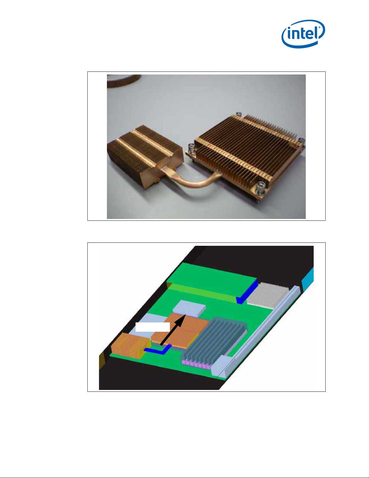
Airflow
direction
Thermal Solutions
Figure 7-7. UP ATCA Thermal Solution
Note: Thermal sample only, retention not production ready.
Figure 7-8. UP ATCA System Layout
Note: Heatsink should be optimized for the layout.
August 2010 Thermal/Mechanical Design Guide
Order Number: 323107-002US 64
Intel® Xeon® Processor C5500/C3500 Series and LGA1366 Socket
Page 65

Figure 7-9. UP ATCA Heat Sink Drawing
Thermal Solutions
§
®
Xeon® Processor C5500/C3500 Series and LGA1366 Socket
Intel
Thermal/Mechanical Design Guide August 2010
65 Order Number: 323107-002US
Page 66
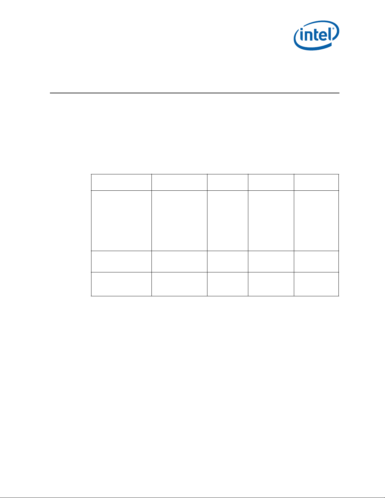
Quality and Reliability Requirements
8 Quality and Reliability
Requirements
8.1 Use Conditions
Intel evaluates reliability performance based on the use conditions (operating
environment) of the end product by using acceleration models.
The use condition environment definitions provided in Table 8-1 and Table 8-2 are
based on speculative use condition assumptions, and are provided only as examples.
Table 8-1. Server Use Conditions Environment (System Level)
Use Environment
Slow small internal
gradient changes due to
external ambient
(temperature cycle or
externally heated).
Fast, large gradient on/
off to max operating
temp. (power cycle or
internally heated
including power save
features)
High ambient moisture
during low-power state
(operating voltage)
High operating
temperature and short
duration high
temperature exposures
Speculative Stress
Condition
Temperature Cycle
THB/HAST T = 25 –30° C
Bake T = 95 - 105° C
Example Use
Condition
ΔT = 35 - 44° C
(solder joint)
85% RH
(ambient)
(contact)
Example 7-Yr
Stress Equiv.
550-930 cycles
Temp Cycle Q
(-25° C to
100° C)
110-220 hrs at
110° C 85% RH
700 – 2500 hrs at
125° C
Example 10-Yr
Stress Equiv.
780-1345 cycles
Temp Cycle Q
(-25° C to
100°C )
145-240 hrs at
110° C 85% RH
800 – 3300 hrs at
125° C
August 2010 Thermal/Mechanical Design Guide
Order Number: 323107-002US 66
Intel® Xeon® Processor C5500/C3500 Series and LGA1366 Socket
Page 67
Quality and Reliability Requirements
Table 8-2. Server Use Conditions Environment (System Level)
Use Environment Speculative Stress Condition Example Use Condition
Shipping and Handling Mechanical Shock
• System-level
•Unpackaged
•Trapezoidal
• 25 g
• velocity change is based on packaged weight
Product weight (lbs) Non-palletized product
< 20 lbs
20 to > 40
40 to > 80
80 to < 100
100 to < 120
≥120
Change in velocity is based upon a 0.5 coefficien t of
restitution.
Shipping and Handling Random Vibration
• System Level
•Unpackaged
• 5 Hz to 500 Hz
• 2.20 g RMS random
• 5 Hz @ .001 g
(slope up)
• 20 Hz to 500 Hz @ 0.01 g
• Random control limit tolerance is ± 3 dB
velocity change (in/sec)
250
225
205
175
145
125
2
/Hz to 20 Hz @ 0.01 g2/Hz
2
/Hz (flat)
Total of 12 drops per
system:
•2 drops per axis
•± direction
Total per system:
• 10 minutes per axis
•3 axes
8.2 Intel Reference Component Validation
Intel tests reference components individually and as an assembly on mechanical test
boards and assesses performance to the envelopes specified in previous sections by
varying boundary conditions.
While component validation shows a reference design is tenable for a limited range of
conditions, customers need to assess their specific boundary conditions and perform
reliability testing based on their use conditions.
Intel reference components are also used in board functional tests to assess
performance for specific conditions.
Note: The 1U thermal solution was tested but the ATCA solution was not fully tested.
8.2.1 Board Functional Test Sequence
Each test sequence should start with components (baseboard, heatsink assembly, and
so on) that have not been previously submitted to any reliability testing.
The test sequence should always start with a visual inspection after assembly, and
BIOS/Processor/memory test. The stress test should be then followed by a visual
inspection and then BIOS/processor/memory test.
®
Xeon® Processor C5500/C3500 Series and LGA1366 Socket
Intel
Thermal/Mechanical Design Guide August 2010
67 Order Number: 323107-002US
Page 68

Quality and Reliability Requirements
8.2.2 Post-Test Pass Criteria
The post-test pass criteria are:
• No significant physical damage to the heatsink and retention hardware.
• Heatsink remains seated and its bottom remains mated flat against the IHS
surface. No visible gap between the heatsink base and processor IHS. No visible tilt
of the heatsink with respect to the retention hardware.
• No signs of physical damage on baseboard surface due to impact of heatsink.
• No visible physical damage to the processor package.
• Successful BIOS/processor/memory test of post-test samples.
• Thermal compliance testing to demonstrate that the case temperature specification
can be met.
8.2.3 Recommended BIOS/Processor/Memory Test Procedures
This test ensures proper operation of the product before and after environmental
stresses, with the thermal mechanical enabling components assembled. The test shall
be conducted on a fully operational baseboard that has not been exposed to any
battery of tests prior to the test being considered.
Test setup should include the following components, properly assembled and/or
connected:
• Appropriate system baseboard.
• Processor and memory.
• All enabling components, including socket and thermal solution parts.
The pass criterion is that the system under test shall successfully complete the
checking of BIOS, basic processor functions, and memory, without any errors. Intel PC
Diags is an example of software that can be utilized for this test.
8.3 Material and Recycling Requirements
Material shall be resistant to fungal growth. Examples of non-resistant materials
include cellulose materials, animal and vegetable based adhesives, grease, oils, and
many hydrocarbons. Synthetic materials such as PVC formulations, certain
polyurethane compositions (for example, polyester and some polyethers), plastics
which contain organic fillers of laminating materials, paints, and varnishes also are
susceptible to fungal growth. If materials are not fungal growth resistant, then MILSTD-810E, Method 508.4 must be performed to determine material performance.
Any plastic component exceeding 25 gm should be recyclable per the European Blue
Angel recycling standards.
The following definitions apply to the use of the terms lead-free, Pb-free, and RoHS
compliant.
Lead-free and Pb-free: Lead has not been intentionally added, but lead may still
exist as an impurity below 1000 ppm.
August 2010 Thermal/Mechanical Design Guide
Order Number: 323107-002US 68
Intel® Xeon® Processor C5500/C3500 Series and LGA1366 Socket
Page 69

Quality and Reliability Requirements
RoHS compliant: Lead and other materials banned in RoHS Directive are either
(1) below all applicable substance thresholds as proposed by the EU or (2) an
approved/pending exemption applies.
Note: RoHS implementation details are not fully defined and may change.
§
®
Xeon® Processor C5500/C3500 Series and LGA1366 Socket
Intel
Thermal/Mechanical Design Guide August 2010
69 Order Number: 323107-002US
Page 70

Component Suppliers
A Component Suppliers
The part numbers below represent Intel reference designs and collaborative designs for
1U and AT CA heatsinks. These components are still in development and might not meet
the criteria in Section 8. Customer implementation of these components may be unique
and require validation by the customer. Customers can obtain these components
directly from the suppliers below.
Table A-1. Heatsinks and Thermal Interface Material
Component Description Supplier PN Supplier Contact Info
1U Reference
Heatsink
p/n E32409-001
ATCA
Reference
heatsink
p/n E65918-001
Thermal
Interface
Material
1U Aluminum
Fin, Copper Base
AT CA Copper Fin,
Copper Base
Phase Change Honeywell
Fujikura
HSA-8078 Rev A
Fujikura
HSA-7901-B
PCM45F
Fujikura America
Yuji Yasuda
yuji@fujikura.com
408-988-7478
Fujikura Taiwan Branch
Yao-Hsien Huang
yeohsien@fujikuratw.com.tw
886(2)8788-4959
Fujikura America
Yuji Yasuda
yuji@fujikura.com
408-748-6991
Fujikura Taiwan Branch
Yao-Hsien Huang
yeohsien@fujikuratw.com.tw
886(2)8788-4959
Scott Miller
509-252-2206
scott.miller4@honeywell.com
Paula Knoll
858-279-2956
paula_knoll@honeywell.com
Note: Performance targets for heatsinks are described in Section 7.1. Mechanical drawings
are provided in Appendix B. Mechanical models are listed in Table 1-1. Heatsinks
assemble to server back plate (Table A-2).
August 2010 Thermal/Mechanical Design Guide
Order Number: 323107-002US 70
Intel® Xeon® Processor C5500/C3500 Series and LGA1366 Socket
Page 71
Component Suppliers
Table A-2. LGA1366 Socket and ILM Components
Item Intel PN Foxconn Tyco
ILM Cover Assembly D92428-002 PT44L12-4101 1939738-1
Server Back Plate D92433-002 PT44P12-4101 1981467-1
LGA1366 Socket D86205-002 PE136627-4371-01F 1939737-1 or 1981837 -1
Supplier Contact Info
Julia Jiang
juliaj@foxconn.com
408-919-6178
Billy Hsieh
billy.hsieh@tycoelectronics.com
+81 44 844 8292
Note: The LGA1366 socket and ILM components are described in Section 2 and Section 3,
respectively. Socket mechanical drawings are provided in Appendix B. Mechanical
models are listed in Table 1-1.
§
®
Xeon® Processor C5500/C3500 Series and LGA1366 Socket
Intel
Thermal/Mechanical Design Guide August 2010
71 Order Number: 323107-002US
Page 72
Mechanical Drawings
B Mechanical Drawings
Table B-1. Mechanical Drawing List
Description Figure
Board Keepin / Keepout Zones (Sheet 1 of 4) Figure B-1
Board Keepin / Keepout Zones (Sheet 2 of 4) Figure B-2
Board Keepin / Keepout Zones (Sheet 3 of 4) Figure B-3
Board Keepin / Keepout Zones (Sheet 4 of 4) Figure B-4
1U Reference Heatsink Assembly (Sheet 1 of 2) Figure B-5
1U Reference Heatsink Assembly (Sheet 2 of 2) Figure B-6
1U Reference Heatsink Fin and Base (Sheet 1 of 2) Figure B-7
1U Reference Heatsink Fin and Base (Sheet 2 of 2) Figure B-8
Heatsink Shoulder Screw (1U, 2U, and Tower) Figure B-9
Heatsink Compression Spring (1U, 2U, and Tower) Figure B-10
Heatsink Retaining Ring (1U, 2U, and Tower) Figure B-11
Heatsink Load Cup (1U, 2U, and Tower) Figure B-12
ATCA Reference Heatsink Assembly (Sheet 1 of 2) Figure B-13
ATCA Reference Heatsink Assembly (Sheet 2 of 2) Figure B-14
ATCA Reference Heatsink Fin and Base (Sheet 1 of 2) Figure B-15
ATCA Reference Heatsink Fin and Base (Sheet 2 of 2) Figure B-16
August 2010 Thermal/Mechanical Design Guide
Order Number: 323107-002US 72
Intel® Xeon® Processor C5500/C3500 Series and LGA1366 Socket
Page 73
Figure B-1. Board Keepin / Keepout Zones (Sheet 1 of 4)
13
4
5678
B
C
D
A
123
4
5678
B
C
D
A
2200 MISSION COLLEGE BLVD.
P.O. BOX 58119
SANTA CLARA, CA 95052-8119
R
49.90
[1.965]
SOCKET BODY OUTLINE,
FOR REFERENCE ONLY
44.70
[1.760]
CENTERLINE OF OUTER
SOCKET BALL ARRAY
47.50
[1.870]
SOCKET BODY OUTLINE,
FOR REFERENCE ONLY
41.66
[1.640]
CENTERLINE OF OUTER
SOCKET BALL ARRAY
36.00
[1.417]
SOCKET ILM
HOLE PATTERN
90.00
[3.543]
MAX THERMAL
RETENTION OUTLINE
90.00
[3.543]
MAX THERMAL
RETENTION OUTLINE
61.20
[2.409]
SOCKET ILM
HOLE PATTERN
80.00
[3.150]
THERMAL RETENTION
HOLE PATTERN
80.00
[3.150]
THERMAL RETENTION
HOLE PATTERN
D77712
102
DWG. NO SHT. REV
SHEET 1 OF 4DO NOT SCALE DRAWINGSCALE: 3.000
02
D77712
D
REV
DRAWING NUMBER
SIZE
THURLEY & GAINESTOWN
ENABLING KEEPIN / KEEPOUT
TITLE
EASD / PTMI
DEPARTMENT
FINISHMATERIAL DATEAPPROVED BY
--
11/03/06J. WILLIAMS
DATECHECKED BY
09/28/06 N. ULEN
DATEDRAWN BY
09/28/06 N. ULEN
DATEDESIGNED BY
UNLESS OTHERWISE SPECIFIED
INTERPRET DIMENSIONS AND TOLERANCES
IN ACCORDANCE WITH ASME Y14.5-1994
DIMENSIONS ARE IN MILLIMETERS
TOLERANCES:
.X # 0.0 Angles # 0.0
.XX # 0.00
.XXX # 0.000
THIRD ANGLE PROJECTION
THIS DRAWING CONTAINS INTEL CORPORAT ION CONFIDENTIAL INFORMATION. IT IS DISCLOSED IN CONFIDENCE AND ITS CONT ENTS
MAY NOT BE DISCLOSED, REPRODUCED, DI SPLAYED OR MODIFIED, WITHOUT THE PRI OR WRITTEN CONSENT OF INTEL CORPORAT ION.
AS VIEWED FROM PRIMARY SIDE
OF THE MOTHERBOARD
NOTES: 1. THIS DRAWING TO BE USED IN CORELATION WITH SUPPLIED
3D DATA BASE FILE. ALL DIMENSIONS AND TOLERANCES
ON THIS DRAWING TAKE PRECEDENCE OVER SUPPLIED FILE.
2. PRIMARY DIMENSIONS STATED IN MILLIMETERS. [BRACKATED]
DIMENSIONS STATED IN INCHES
3. SOCKET KEEP OUT DIMENSIONS SHOWN FOR REFERNCE ONLY
PLEASE REFER TO THE SOCKET B KEEPOUT / KEEPIN DRAWING
FOR EXACT DIMENSIONS
4 BALL 1 LOCATION WITH RESPECT TO SOCKET BALL ARRAY IS
FORMED BY INTERSECTION OF ROW A & COLUMN 1. MAXIMUM
OUTLINE OF SOCKET SOLDERBALL ARRAY MUST BE PLACED
SYMMETRIC TO THE ILM HOLE PATTERN (INNER PATTERN) FOR
PROPER ILM & SOCKET FUNCTION.
5. A HEIGHT RESTRICTION ZONE IS DEFINED AS ONE WHERE
ALL COMPONENTS PLACED ON THE SURFACE OF THE MOTHERBOARD
MUST HAVE A MAXIMUM HEIGHT NO GREATER THAN THE HEIGHT
DEFINED BY THAT ZONE.
ALL ZONES DEFINED WITHIN THE 90 X 90 MM
OUTLINE REPRESENT SPACE THAT RESIDES BENEATH THE HEAT
SINK FOOTPRINT.
UNLESS OTHERWISE NOTED ALL VIEW DIMENSION ARE NOMINAL.
ALL HEIGHT RESTRICTIONS ARE MAXIMUMS. NEITHER ARE
DRIVEN BY IMPLIED TOLERANCES.
A HEIGHT RESTRICTION OF 0.0 MM REPRESENTS
THE TOP (OR BOTTOM) SURFACE OF THE MOTHERBOARD AS
THE MAXIMUM HEIGHT.
SEE NOTE 7 FOR ADDITIONAL DETAILS.
6. SEE SHEET 4 FOR REVISION HISTORY.
7 COMBINED COMPONENT AND SOLDER PASTE HEIGHT INCLUDING
TOLERANCES AFTER REFLOW.
BALL 1 POSITION 4
LINE REPRESENTS OF
OUTERMOST ROWS AND COLUMNS
OF SOCKET BALL ARRAY OUTLINE.
FOR REFERENCE ONLY
SOCKET BODY OUTLINE
FOR REFERENCE ONLY
LEGEND, THIS SHEET ONLY
ZONE 1:
0.0 MM MAX COMPONENT HEIGHT, NO COMPONENT PLACEMENT,
SOCKET, ILM, AND FINGER ACCESS KEEPIN ZONE
ZONE 2:
7.0 MM MAX COMPONENT HEIGHT 7
ZONE 3:
3.0 MM MAX COMPONENT HEIGHT 7
ZONE 4:
0.0 MM MAX COMPONENT HEIGHT, NO COMPONENT PLACEMENT
RETENTION MODULE OR HEAT SINK TOUCH ZONE
ZONE 5:
0.0 MM MAX COMPONENT HEIGHT, NO COMPONENT PLACEMENT,
NO ROUTE ZONE
ZONE 6:
1.97 MM MAX COMPONENT HEIGHT, SOCKET CAVITY 7
Mechanical Drawings
®
Xeon® Processor C5500/C3500 Series and LGA1366 Socket
Intel
Thermal/Mechanical Design Guide August 2010
73 Order Number: 323107-002US
Page 74

13
4
5678
B
C
D
A
123
4
5678
B
C
D
A
2200 MISSION COLLEGE BLVD.
P.O. BOX 58119
SANTA CLARA, CA 95052-8119
R
2X 0.00
0.000[]
2X 0.00
0.000[]
2X 7.50
0.295[]
9.60
0.378[]
12.30
0.484[]
67.70
2.665[]
2X 72.50
2.854[]
32.85
1.293[]
47.15
1.856[]
BALL 1 4
19.17
0.755[]
3.30
0.130[]
29.90
1.177[]
BALL 1 4
62.39
2.456[]
77.90
3.067[]
30.600
1.205[]
49.40
1.945[]
4X NPTH
THERMAL RETENTION
MOUNTING HOLES
4.03
+0.06
-0.03
0.159
+0.002
-0.001
[]
4X NPTH
SOCKET ILM
MOUNTING HOLES
3.80
+0.06
-0.03
0.150
+0.002
-0.001[]
4X
NO ROUTE
COPPER PAD ON SURFACE
6.00
0.236[]
4X 6.00
0.236[]
2X 9.400
0.3701[]
9.900
0.3898[]
2X 70.600
2.7795[]
22.000
0.8661[]
58.000
2.2835[]
2X 7.50
0.295[]
2X 72.50
2.854[]
85.00
3.346[]
5.00
0.197[]
5.00
0.197[]
85.00
3.346[]
2X 80.00
3.150[]
3X 80.00
3.150[]
D77712 2 02
DWG. NO SHT. REV
THIS DRAWING CONTAINS INTEL CORPORAT ION CONFIDENTIAL INFORMATION. IT IS DISCLOSED IN CONFIDENCE AND ITS CONT ENTS
MAY NOT BE DISCLOSED, REPRODUCED, DI SPLAYED OR MODIFIED, WITHOUT THE PRI OR WRITTEN CONSENT OF INTEL CORPORAT ION.
SHEET 2 OF 4DO NOT SCALE DRAWINGSCALE: 3.000
EASD / PTMI
02D77712D
REVDRAWING NUMBERSIZEDEPARTMENT
AS VIEWED FROM PRIMARY SIDE
OF THE MOTHERBOARD
(DETAILS)
SEE DETAIL A
DETAIL A
SCALE 6.000
LEGEND, THIS SHEET ONLY
ZONE 1:
0.0 MM MAX COMPONENT HEIGHT, NO COMPONENT PLACEMENT,
SOCKET, ILM, AND FINGER ACCESS KEEPIN ZONE
ZONE 2:
7.0 MM MAX COMPONENT HEIGHT 7
ZONE 3:
3.0 MM MAX COMPONENT HEIGHT 7
ZONE 4:
0.0 MM MAX COMPONENT HEIGHT, NO COMPONENT PLACEMENT
RETENTION MODULE OR HEAT SINK TOUCH ZONE
ZONE 5:
0.0 MM MAX COMPONENT HEIGHT, NO COMPONENT PLACEMENT,
NO ROUTE ZONE
ZONE 6:
1.97 MM MAX COMPONENT HEIGHT, SOCKET CAVITY 7
Mechanical Drawings
Figure B-2. Board Keepin / Keepout Zones (Sheet 2 of 4)
August 2010 Thermal/Mechanical Design Guide
Order Number: 323107-002US 74
Intel® Xeon® Processor C5500/C3500 Series and LGA1366 Socket
Page 75

Figure B-3. Board Keepin / Keepout Zones (Sheet 3 of 4)
13
4
5678
B
C
D
A
123
4
5678
B
C
D
A
2200 MISSION COLLEGE BLVD.
P.O. BOX 58119
SANTA CLARA, CA 95052-8119
R
8X 6.00
0.236[]
5.00
0.197[]
5.00
0.197[]
0.00
0.000[]
0.00
0.000[]
5.00
0.197[]
17.17
0.676[]
62.83
2.474[]
75.00
2.953[]
85.00
3.346[]
9.50
0.374[]
32.85
1.293[]
47.15
1.856[]
70.50
2.776[]
85.00
3.346[]
30.60
1.205[]
49.40
1.945[]
(90.00 )
[3.543]
(90.00 )
[3.543]
(72.20 )
[2.843]
(47.00 )
[1.850]
D77712 3 02
DWG. NO SHT. REV
THIS DRAWING CONTAINS INTEL CORPORAT ION CONFIDENTIAL INFORMATION. IT IS DISCLOSED IN CONFIDENCE AND ITS CONT ENTS
MAY NOT BE DISCLOSED, REPRODUCED, DI SPLAYED OR MODIFIED, WITHOUT THE PRI OR WRITTEN CONSENT OF INTEL CORPORAT ION.
SHEET 3 OF 4DO NOT SCALE DRAWINGSCALE: 3.000
EASD / PTMI
02D77712 D
REVDRAWING NUMBERSIZEDEPARTMENT
AS VIEWED FROM SECONDARY SIDE
OF THE MOTHERBOARD
(DETAILS)
DESKTOP BACKPLATE
KEEPIN SHOWN FOR
REFERENCE ONLY
LEGEND, THIS SHEET ONLY
ZONE 7:
NO COMPONENT PLACEMENT, STIFFENING PLATE CONTACT AREA
ZONE 8:
1.8 MM MAX COMPONENT HEIGHT 7
ZONE 9:
NO COMPONENT PLACEMENT & NO ROUTE ZONE
Mechanical Drawings
®
Xeon® Processor C5500/C3500 Series and LGA1366 Socket
Intel
Thermal/Mechanical Design Guide August 2010
75 Order Number: 323107-002US
Page 76

13
4
5678
B
C
D
A
123
4
5678
B
C
D
A
2200 MISSION COLLEGE BLVD.
P.O. BOX 58119
SANTA CLARA, CA 95052-8119
R
REVISION HISTORY
ZONE REV DESCRIPTION DATE APPROVED
-
A ORIGINAL RELEASE 09/29/06-B
M.B COMPONENT HEIGHT RESTRICTION
CHANGED FROM 2.5MM TO 7MM
10/05/06
C ADDED ADDITION KO FOR RM, SHEET 1 10/27/06
D
DRAWING RE-DO, ADDED BALL PATTERN, SOCKET
BODY, BALL 1, BACKSIDE WINDOW, GENERAL
DRAWING CLARIFICATIONS.
11/03/06
E UPDATED SOCKET KEEPIN OUTLINE TO REFLECT
RECENT CHANGES. SEE KEEPIN ZONE 1
OUTLINE, SHEETS 1 & 2.
11/30/06
2D3 2C1
F CORRECTED ILM HOLE DIAMETER. WAS SHOWING
RADIUS VALUE. 1.9 --> 3.8
UPDATED BACKPLATE HOLE DIAMTER SIZE FOR DT
COMPATIBILITY. DIAMETER 4.0 --> 4.03
12/18/06
G REMOVED 3.0 MM HEIGHT RESTRICTION ZONE
TO THE LEFT AND RIGHT OF SOCKET OUTLINE
01/12/07
1C6
1B5
2B8
2D6
2D4
H MOVED REVISION HISTORY TABLE TO SHEET 4
CORRECTED SOCKET SOLDERBALL ARRAY & POS
41.66 --> 40.64 (ARRAY SIZE)
44.85 --> 44.70 (ARRAY SIZE)
62.43 --> 62.39 (ARRAY POSITION)
19.17 --> 19.67 (ARRAY POSITION)
ADDED TOPSIDE CU PAD CALLOUT FOR ILM HOLES
SEE DETAIL A, SHEET 2
01/19/07
1C6
2D6
I REVERTED SOCKET SOLDERBALL ARRAY
X DIRECTION SIZE AND POSITION TO REV G.
40.64 --> 41.66 (ARRAY WIDTH)
19.67 --> 19.17 (ARRAY POSITION)
SOLDERBALL ARRAY OUTLINE REPRESENTS THE
CENTERLINE OF THE OUTER BALL ROWS/COLS
01/22/07
SHT 4
SHT 4
SHT 3 SHT 1
J ADDED ISO VIEW OF SECONDARY SIDE
MOVED ISO VEWS TO SHEET 4
MODIFIED BACKSIDE HEIGHT RESTRICTIONS FOR
NEW BACKPLATE GEOMETRY
ADDED NOTE 5 DETAILING HEIGHT RESTRICTION
NOMENCLATURE
REMOVED TOLERANCE BLOCK VALUES,
SEE NOTE 5
02/06/07
K UPDATED ZONE 1 KEEPOUT ON SHEETS 1 & 2
TO ALLOW MORE SOCKET LEVER ARM ACCESS,
LEFT SIDE OF ZONE
02/27/07
01 PRODUCTION RELEASE 08/02/07
02 ZONE 6 HEIGHT FROM 1.8MM --> 1.97MM
ADDED NOTE 7
02/24/09
D77712 4 02
DWG. NO SHT. REV
THIS DRAWING CONTAINS INTEL CORPORAT ION CONFIDENTIAL INFORMATION. IT IS DISCLOSED IN CONFIDENCE AND ITS CONT ENTS
MAY NOT BE DISCLOSED, REPRODUCED, DI SPLAYED OR MODIFIED, WITHOUT THE PRI OR WRITTEN CONSENT OF INTEL CORPORAT ION.
SHEET 4 OF 4DO NOT SCALE DRAWINGSCALE: 2.500
EASD / PTMI
02
D77712D
REVDRAWING NUMBERSIZEDEPARTMENT
ALL ZONES, SEE NOTE 5
THIS HEIGHT REPRESENTS AN ARBITRARY
MOTHERBOARD THICKNESS
SECONDARY SIDE
3D HEIGHT RESTRICTION ZONES
PRIMARY SIDE
3D HEIGHT RESTRICTION ZONES
Mechanical Drawings
Figure B-4. Board Keepin / Keepout Zones (Sheet 4 of 4)
August 2010 Thermal/Mechanical Design Guide
Order Number: 323107-002US 76
Intel® Xeon® Processor C5500/C3500 Series and LGA1366 Socket
Page 77

Figure B-5. 1U Reference Heatsink Assembly (Sheet 1 of 2)
ASSEMBLY, HEAT SINK, 1U
Mechanical Drawings
®
Xeon® Processor C5500/C3500 Series and LGA1366 Socket
Intel
Thermal/Mechanical Design Guide August 2010
77 Order Number: 323107-002US
Page 78

Mechanical Drawings
Figure B-6. 1U Reference Heatsink Assembly (Sheet 2 of 2)
August 2010 Thermal/Mechanical Design Guide
Order Number: 323107-002US 78
Intel® Xeon® Processor C5500/C3500 Series and LGA1366 Socket
Page 79

Figure B-7. 1U Reference Heatsink Fin and Base (Sheet 1 of 2)
Mechanical Drawings
®
Xeon® Processor C5500/C3500 Series and LGA1366 Socket
Intel
Thermal/Mechanical Design Guide August 2010
79 Order Number: 323107-002US
Page 80
Mechanical Drawings
Figure B-8. 1U Reference Heatsink Fin and Base (Sheet 2 of 2)
August 2010 Thermal/Mechanical Design Guide
Order Number: 323107-002US 80
Intel® Xeon® Processor C5500/C3500 Series and LGA1366 Socket
Page 81
Figure B-9. Heatsink Shoulder Screw (1U, 2U, and Tower)
Mechanical Drawings
®
Xeon® Processor C5500/C3500 Series and LGA1366 Socket
Intel
Thermal/Mechanical Design Guide August 2010
81 Order Number: 323107-002US
Page 82

Mechanical Drawings
Figure B-10. Heatsink Compression Spring (1U, 2U, and Tower)
August 2010 Thermal/Mechanical Design Guide
Order Number: 323107-002US 82
Intel® Xeon® Processor C5500/C3500 Series and LGA1366 Socket
Page 83
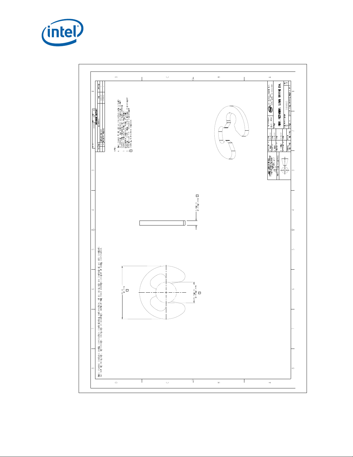
Figure B-11. Heatsink Retaining Ring (1U, 2U, and Tower)
Mechanical Drawings
®
Xeon® Processor C5500/C3500 Series and LGA1366 Socket
Intel
Thermal/Mechanical Design Guide August 2010
83 Order Number: 323107-002US
Page 84
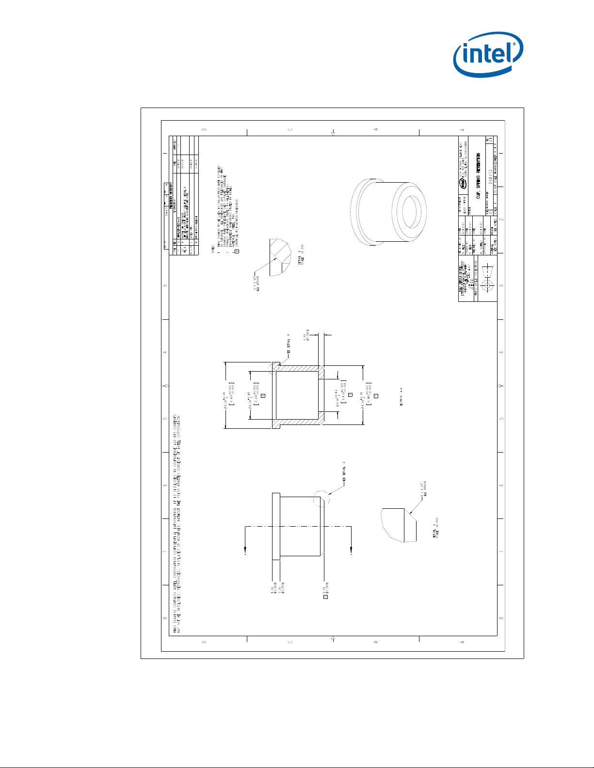
Mechanical Drawings
Figure B-12. Heatsink Load Cup (1U, 2U, and Tower)
August 2010 Thermal/Mechanical Design Guide
Order Number: 323107-002US 84
Intel® Xeon® Processor C5500/C3500 Series and LGA1366 Socket
Page 85
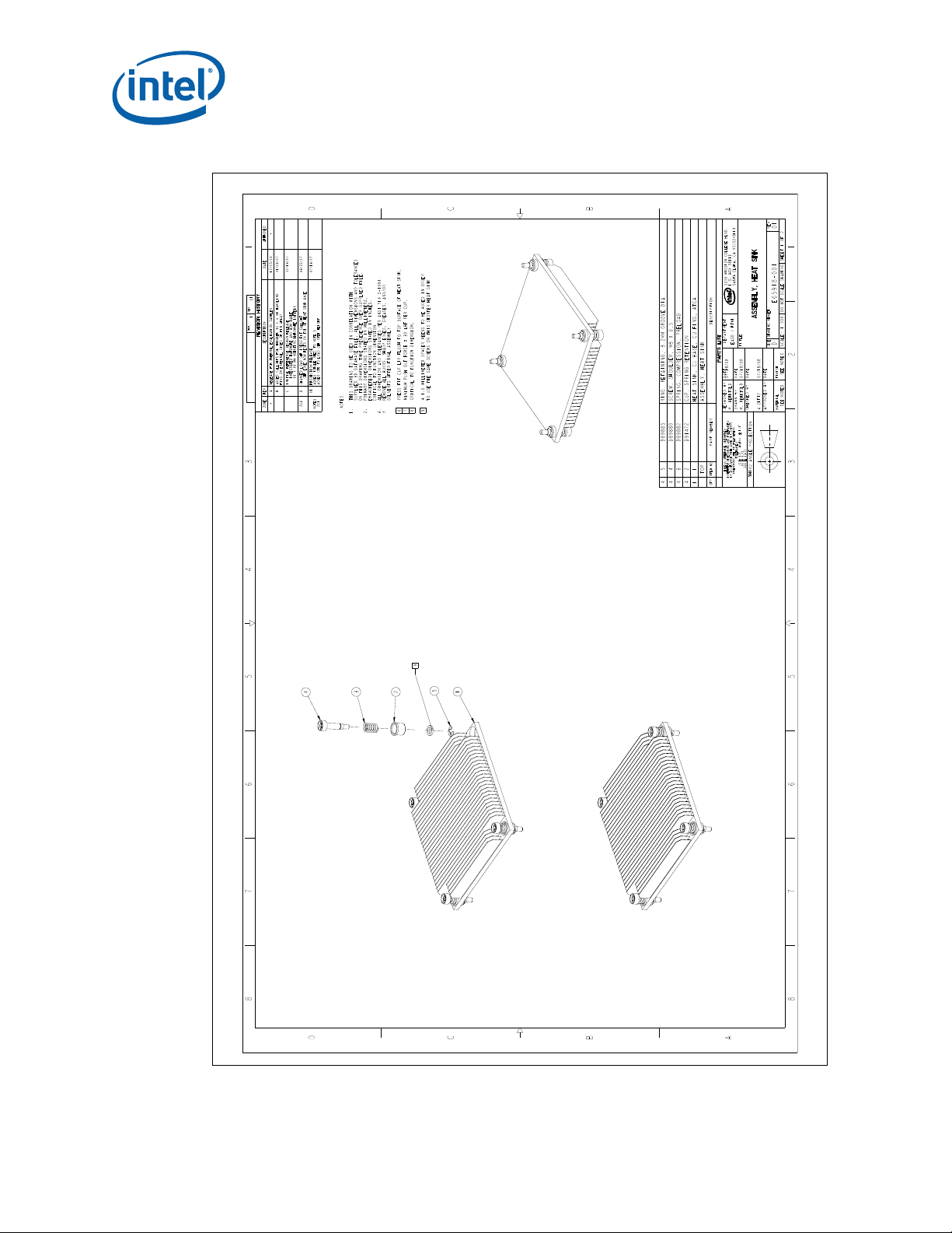
Figure B-13. ATCA Reference Heatsink Assembly (Sheet 1 of 2)
Mechanical Drawings
®
Xeon® Processor C5500/C3500 Series and LGA1366 Socket
Intel
Thermal/Mechanical Design Guide August 2010
85 Order Number: 323107-002US
Page 86
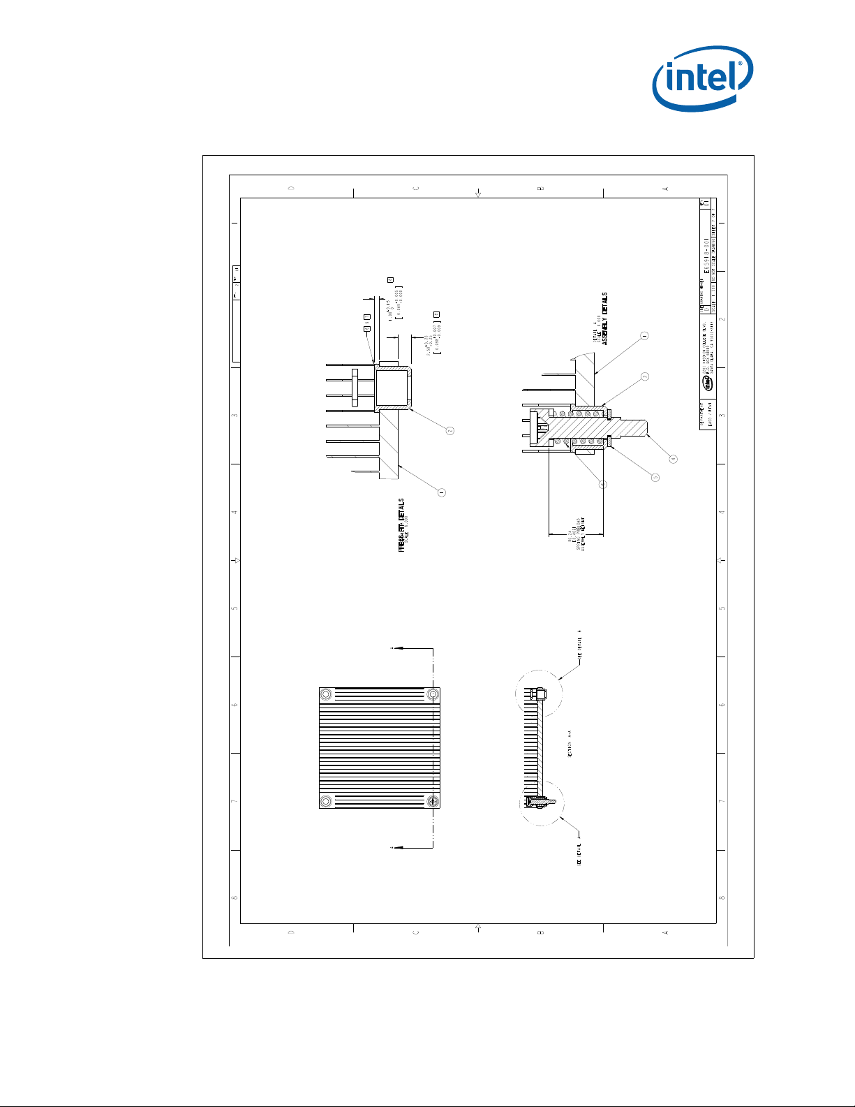
Mechanical Drawings
Figure B-14. ATCA Reference Heatsink Assembly (Sheet 2 of 2)
August 2010 Thermal/Mechanical Design Guide
Order Number: 323107-002US 86
Intel® Xeon® Processor C5500/C3500 Series and LGA1366 Socket
Page 87
Figure B-15. ATCA Reference Heatsink Fin and Base (Sheet 1 of 2)
Mechanical Drawings
®
Xeon® Processor C5500/C3500 Series and LGA1366 Socket
Intel
Thermal/Mechanical Design Guide August 2010
87 Order Number: 323107-002US
Page 88
Mechanical Drawings
Figure B-16. ATCA Reference Heatsink Fin and Base (Sheet 2 of 2)
August 2010 Thermal/Mechanical Design Guide
Order Number: 323107-002US 88
Intel® Xeon® Processor C5500/C3500 Series and LGA1366 Socket
Page 89
Socket Mechanical Drawings
C Socket Mechanical Drawings
Table C-1 lists the mechanical drawings included in this appendix.
Table C-1. Mechanical Drawing List
Drawing Description Figure Number
“Socket Mechanical Drawing - (Sheet 1 of 4)” Figure C-1
“Socket Mechanical Drawing - (Sheet 2 of 4)” Figure C-2
“Socket Mechanical Drawing - (Sheet 3 of 4)” Figure C-3
“Socket Mechanical Drawing - (Sheet 4 of 4)” Figure C-4
August 2010 Thermal/Mechanical Design Guide
Order Number: 323107-002US 89
Intel® Xeon® Processor C5500/C3500 Series and LGA1366 Socket
Page 90

Figure C-1. Socket Mechanical Drawing - (Sheet 1 of 4)
Socket Mechanical Drawings
®
Xeon® Processor C5500/C3500 Series and LGA1366 Socket
Intel
Thermal/Mechanical Design Guide August 2010
90 Order Number: 323107-002US
Page 91
Socket Mechanical Drawings
Figure C-2. Socket Mechanical Drawing - (Sheet 2 of 4)
August 2010 Thermal/Mechanical Design Guide
Order Number: 323107-002US 91
Intel® Xeon® Processor C5500/C3500 Series and LGA1366 Socket
Page 92

Figure C-3. Socket Mechanical Drawing - (Sheet 3 of 4)
Socket Mechanical Drawings
®
Xeon® Processor C5500/C3500 Series and LGA1366 Socket
Intel
Thermal/Mechanical Design Guide August 2010
92 Order Number: 323107-002US
Page 93

Socket Mechanical Drawings
Figure C-4. Socket Mechanical Drawing - (Sheet 4 of 4)
§
August 2010 Thermal/Mechanical Design Guide
Order Number: 323107-002US 93
Intel® Xeon® Processor C5500/C3500 Series and LGA1366 Socket
 Loading...