

Page 1

SPSH4 Server System
Technical Product Specification
Intel reference number 10736
Revision 1.11
March, 2003
Enterprise Platforms and Services Marketing
Page 2
Revision History SPSH4 Server System Technical Product Specification
Revision History
Date Revision
Number
6/21/01 0.5 Preliminary Draft for Review
8/20/02 1.0 Revisions to Roll to 1.0 for publication
1/2003 1.1 Revisions to include Adaptec U320 SCSI Controller 100 MHz support
March
2003
1.11 Corrected section 5.3.4 on page 45 to reflect 4Mb Video rather than 2 mb video
memory to be consistent with the SRSH4 TPS
Modifications
Revision 1.11
ii
Page 3

SPSH4 Server System Technical Product Specification Disclaimers
Disclaimers
Information in this document is provided in connection with Intel® products. No license, express
or implied, by estoppel or otherwise, to any intellectual property rights is granted by this
document. Except as provided in Intel's Terms and Conditions of Sale for such products, Intel
assumes no liability whatsoever, and Intel disclaims any express or implied warranty, relating to
sale and/or use of Intel products including liability or warranties relating to fitness for a particular
purpose, merchantability, or infringement of any patent, copyright or other intellectual property
right. Intel products are not intended for use in medical, life saving, or life sustaining
applications. Intel may make changes to specifications and product descriptions at any time,
without notice.
Designers must not rely on the absence or characteristics of any features or instructions marked
"reserved" or "undefined." Intel reserves these for future definition and shall have no
responsibility whatsoever for conflicts or incompatibilities arising from future changes to them.
This document contains information on products in the design phase of development. Do not
finalize a design with this information. Revised information will be published when the product is
available. Verify with your local sales office that you have the latest datasheet before finalizing a
design.
The SPSH4 Server System may contain design defects or errors known as errata which may
cause the product to deviate from published specifications. Current characterized errata are
available on request.
This document and the software described in it is furnished under license and may only be used
or copied in accordance with the terms of the license. The information in this manual is
furnished for informational use only, is subject to change without notice, and should not be
construed as a commitment by Intel Corporation. Intel Corporation assumes no responsibility or
liability for any errors or inaccuracies that may appear in this document or any software that may
be provided in association with this document.
Except as permitted by such license, no part of this document may be reproduced, stored in a
retrieval system, or transmitted in any form or by any means without the express written consent
of Intel Corporation.
Intel, Pentium, Itanium, and Xeon are trademarks or registered trademarks of Intel Corporation.
*Other brands and names may be claimed as the property of others.
Copyright © Intel Corporation 2001.
Revision 1.11
iii
Page 4

Table of Contents SPSH4 Server System Technical Product Specification
Table of Contents
1. Introduction ..........................................................................................................................1
2. SPSH4 Server Chassis Feature Overview.......................................................................... 2
2.1 Front Panel ......................................................................................................................5
2.2 Rear Features..................................................................................................................7
3. Physical Specifications .......................................................................................................9
3.1 SSH4 Boardset ..............................................................................................................11
3.2 Guidelines For Installing Memory in the SSH4 Server Board........................................ 14
4. Power supply Subsystem.................................................................................................. 15
4.1 Mechanical Dimensions................................................................................................. 18
4.2 Airflow Requirements..................................................................................................... 20
4.2.1 Over-Temperature Protection ..................................................................................20
4.2.2 Connectors and Pinouts........................................................................................... 20
4.2.3 AC Electrical Specifications .....................................................................................22
4.2.4 DC Output Specification........................................................................................... 25
4.2.5 Electrical Protection Circuits ....................................................................................32
4.2.6 Control Signals......................................................................................................... 33
4.3 Cooling Subsystem........................................................................................................ 38
4.3.1 Redundancy and Ambient Temperature Control...................................................... 38
4.3.2 Cooling Summary..................................................................................................... 39
5. Cables and Connectors ..................................................................................................... 40
5.1 Interconnect Block Diagram........................................................................................... 40
5.2 Cable and Interconnect Descriptions............................................................................. 41
5.3 Operator-Accessible Interconnects................................................................................ 42
5.3.1 Keyboard and Mouse Ports...................................................................................... 42
5.3.2 Serial Ports............................................................................................................... 43
5.3.3 Parallel Port.............................................................................................................. 44
5.3.4 Video Port ................................................................................................................45
5.3.5 Universal Serial Bus (USB) Interface ....................................................................... 45
5.3.6 ICMB Connectors..................................................................................................... 46
5.3.7 100/10 Ethernet Connector (LAN 1)......................................................................... 46
5.3.8 1000/100/10 Ethernet Connector (LAN 2)................................................................ 47
5.3.9 Internal SCA-2 HDD Connector ............................................................................... 47
Revision 1.11
iv
Page 5

SPSH4 Server System External Product Specification Table of Contents
5.3.10 External SCSI......................................................................................................... 49
5.3.11 AC Power Input ...................................................................................................... 50
6. SCSI Bay Boardset............................................................................................................. 51
6.1 Hot Swap Hard Drive Backplane ................................................................................... 51
6.1.1 Architectural Overview ............................................................................................. 52
6.2 Design Constraints and Assumptions............................................................................ 52
6.2.1 SCSI Bus Considerations......................................................................................... 52
6.3 Functional Description ................................................................................................... 53
6.3.1 Wide SCSI Connector .............................................................................................. 53
6.3.2 SCA-2 Connectors ................................................................................................... 53
6.3.3 SCSI Multi-ModeTermination ...................................................................................54
6.3.4 SCSI Interface.......................................................................................................... 54
6.3.5 Power Control ..........................................................................................................54
6.3.6 FET Short Protection................................................................................................ 54
6.3.7 Microcontroller.......................................................................................................... 55
6.3.8 Device SCSI ID ........................................................................................................ 55
6.3.9 Hard Drive Activity LED............................................................................................ 55
6.3.10 Hard Drive Fault LED ............................................................................................. 56
6.3.11 IMB (I2C bus).......................................................................................................... 56
6.3.12 Fan Support ...........................................................................................................56
6.3.13 Temperature........................................................................................................... 56
6.3.14 Serial EEPROM......................................................................................................56
6.4 Board Functions............................................................................................................. 57
6.4.1 Reset........................................................................................................................ 57
6.4.2 Microcontroller.......................................................................................................... 57
6.4.3 SCSI Controller ........................................................................................................ 59
6.4.4 Multi-Mode SCSI Termination ..................................................................................59
6.5 Memory Map.................................................................................................................. 59
6.5.1 Memory Map ............................................................................................................ 60
6.5.2 I/O Ports ................................................................................................................... 63
6.6 Programming Information .............................................................................................. 65
6.6.1 Firmware Support Requirements ............................................................................. 66
6.7 External Interface Specifications ...................................................................................66
6.7.1 Connector Specifications .........................................................................................66
6.7.2 SCSI Input Connector 68P....................................................................................... 67
Revision 1.11
Intel reference number 10736
v
Page 6

Table of Contents SPSH4 Server System Technical Product Specification
6.7.3 I2C Connector........................................................................................................... 69
6.7.4 Power Connector .....................................................................................................70
6.7.5 Fan 3-pin Connector ................................................................................................70
6.7.6 SAF-TE PCI Connector Interface............................................................................. 70
6.8 Cables............................................................................................................................ 73
6.8.1 Signal Cables ........................................................................................................... 73
6.8.2 Power Cables........................................................................................................... 73
6.9 Mechanical Specifications .............................................................................................73
7. System Boards ...................................................................................................................75
7.1 Power Distribution Board ...............................................................................................75
7.1.1 Board Layout............................................................................................................ 76
7.1.2 Connector Pinouts.................................................................................................... 76
7.2 Front Panel Board.......................................................................................................... 79
7.2.1 Board Layout............................................................................................................ 80
7.2.2 Connector Pinouts.................................................................................................... 81
7.3 Fan Distribution Board ................................................................................................... 83
7.3.1 Board Layout............................................................................................................ 83
7.3.2 Connector Pinouts.................................................................................................... 83
7.4 HPIB Board.................................................................................................................... 85
7.4.1 Board Layout............................................................................................................ 86
7.4.2 Connector Pinouts.................................................................................................... 86
7.5 ICMB Board ................................................................................................................... 87
7.5.1 Board Layout............................................................................................................ 87
7.5.2 Connector Pinouts.................................................................................................... 87
8. Hardware Configuration .................................................................................................... 89
8.1 System Configuration ....................................................................................................89
8.2 Spares / Accessories ..................................................................................................... 90
9. Product Regulatory Compliance Specifications .............................................................91
9.1 Product Safety Compliance ........................................................................................... 91
9.2 Product EMC Compliance ............................................................................................. 91
9.3 Regulatory Markings...................................................................................................... 92
9.4 Product Safety Markings................................................................................................ 93
9.5 Power supply Regulatory Agency Certifications ............................................................93
9.6 Regulatory Compliance Notices, Statements and Information ......................................94
9.6.1 USA FCC Verification Notice ...................................................................................94
Revision 1.11
vi
Page 7

SPSH4 Server System External Product Specification Table of Contents
9.6.2 Canada..................................................................................................................... 95
9.6.3 European Union ....................................................................................................... 95
9.6.4 Australia / New Zealand ........................................................................................... 95
9.6.5 Japan .......................................................................................................................95
9.6.6 Taiwan...................................................................................................................... 96
9.7 Replacing The Back Up Battery..................................................................................... 96
10. Environmental Specifications ........................................................................................... 97
11. Serviceability and Usability............................................................................................... 98
11.1 Mean Time to Repair.................................................................................................. 98
11.2 Special Usability Features.......................................................................................... 99
12. Index ......................................................................................................................................V
Revision 1.11
Intel reference number 10736
vii
Page 8

List of Figures SPSH4 Server System Technical Product Specification
List of Figures
Figure 1: Front View of Pedestal Configuration ............................................................................ 3
Figure 2: Front View of Rack Configuration .................................................................................. 3
Figure 3: Front View of System (Shown with Bezel Removed)..................................................... 4
Figure 4: Front Panel Details (Rack Bezel Shown)....................................................................... 5
Figure 5: Rear View Of Chassis.................................................................................................... 7
Figure 6: SPSH4 Server System Photograph with Side Panels and Front Panel Removed ......10
Figure 7: Functional Block Diagram of SSH4 Boardset ..............................................................11
Figure 8: SPSH4 Power supply ..................................................................................................16
Figure 9: Rear view of SPSH4 Power Supply Bay...................................................................... 17
Figure 10: SPSH4 Power supply Outline Drawing...................................................................... 19
Figure 11: Connector Pin Locations............................................................................................ 21
Figure 12: Inrush Curve ..............................................................................................................25
Figure 13: Differential Noise Test Setup ..................................................................................... 29
Figure 14: Output Voltage Timing ............................................................................................... 30
Figure 15: Turn On/Off Timing .................................................................................................... 31
Figure 16: Fan Bay (Shown with all Fan Banks Installed) ..........................................................38
Figure 17: SPSH4 System Interconnect Block Diagram............................................................. 40
Figure 18: SCA-2 Connector....................................................................................................... 48
Figure 19: AC Power Input Connector ........................................................................................50
Figure 20: Functional Block Diagram.......................................................................................... 53
Figure 21: Microcontroller Memory Map ..................................................................................... 60
Figure 22: SCSI Input connector 68P Non-Shielded ..................................................................67
Figure 23: SCA-2 Connector 80P ............................................................................................... 68
Figure 24: Hotswap Backplane Mechanical Drawing.................................................................. 73
Figure 25: SAF-TE Addin Card Mechanical Drawing.................................................................. 74
Figure 26: Fan Board Layout ......................................................................................................76
Figure 27: Power supply Mating Connector Pin Locations ......................................................... 77
Figure 28: Fan Board Layout ......................................................................................................80
Figure 29: Fan Board Layout ......................................................................................................83
Figure 30: HPIB Board Layout ....................................................................................................86
Figure 31: ICMB Board Layout ...................................................................................................87
Revision 1.11
viii
Page 9

SPSH4 Server System External Product Specification List of Tables
List of Tables
Table 1: Front Panel Features ...................................................................................................... 6
Table 2: System Features - Rear..................................................................................................8
Table 3: Physical Specifications ...................................................................................................9
Table 4: LED Indicators ..............................................................................................................18
Table 5: Airflow Requirements....................................................................................................20
Table 6: Signal Descriptions .......................................................................................................21
Table 7: Output Connector Pin-out ............................................................................................. 21
Table 8: AC Input Voltage Rating ...............................................................................................22
Table 9: AC Line Sag Transient Performance ............................................................................ 23
Table 10: AC Line Surge Transient Performance .......................................................................23
Table 11: Electrostatic Discharge, IEC 801-2/IEC 1000-4-2....................................................... 23
Table 12: Electrical Fast Transient/Burst, IEC 801-4/IEC 1000-4-4 ...........................................23
Table 13: Radiated Immunity, IEC 801-3/IEC1000-4-3 .............................................................. 23
Table 14: Surge Immunity IEC 1000-4-5 .................................................................................... 24
Table 15: Ring Wave ..................................................................................................................24
Table 16: DC Output Voltage Limits ...........................................................................................26
Table 17: 600W Load Ratings ....................................................................................................27
Table 18: Total System Load at Line AC Input ........................................................................... 27
Table 19: Absolute Worst Case System Power Budget.............................................................. 27
Table 20: Remote Sense Drops.................................................................................................. 28
Table 21: Dynamic Tolerance Requirement ...............................................................................28
Table 22: Ripple and Noise......................................................................................................... 29
Table 23: Output Voltage Timing ................................................................................................ 30
Table 24: Turn On/Off Timing ..................................................................................................... 30
Table 25: Over-Voltage Limits ....................................................................................................32
Table 26: Over Current Protection Limits.................................................................................... 32
Table 27: PSON Signal Characteristic........................................................................................ 33
Table 28: PWOK Signal Characteristics ..................................................................................... 33
Table 29: PSKILL Signal Characteristics .................................................................................... 34
Table 30: FAIL Signal Characteristics......................................................................................... 35
Table 31: PRFL Signal Characteristics ....................................................................................... 35
Table 32: PRESENT# Signal Characteristics .............................................................................. 36
Revision 1.11
Intel reference number 10736
ix
Page 10

List of Tables SPSH4 Server System Technical Product Specification
Table 33: Fan Speed Control......................................................................................................36
Table 34: Pins for Power supply Connector FRU Information .................................................... 37
Table 35: System Interconnect Descriptions ..............................................................................41
Table 36: Keyboard and Mouse Ports ........................................................................................42
Table 37: Serial Port A Connector .............................................................................................. 43
Table 38: Parallel Port Connector...............................................................................................44
Table 39: Video Connector .........................................................................................................45
Table 40: Dual USB Connector................................................................................................... 45
Table 41: ICMB Connector .........................................................................................................46
Table 42: Ethernet Connector.....................................................................................................46
Table 43: Ethernet Connector.....................................................................................................47
Table 44: SCA-2 Connector........................................................................................................47
Table 45: SCSI Connector .......................................................................................................... 49
Table 46: SCSI ID Assignments .................................................................................................55
Table 47: Hard Drive Activity LED ..............................................................................................55
Table 48: Hard Drive Fault LED..................................................................................................56
Table 49: Drive Power Status Byte Format................................................................................. 61
Table 50: Fault Indicator Control Byte Format ............................................................................62
Table 51: Drive Presence Status Byte Format............................................................................ 62
Table 52: P1 Functions ............................................................................................................... 64
Table 53: P3 Functions ............................................................................................................... 65
Table 54: Connector Specifications ............................................................................................ 66
Table 55: SCSI Input connector (J1D1) ...................................................................................... 67
Table 56: SCA-2 Connectors (J3E1, J3D1, J3C1, J3B1, J3A1) ................................................. 68
Table 57: I2C Connector (J2A1) .................................................................................................. 69
Table 58: Power Connector (J4A1, J3A2) ..................................................................................70
Table 59: Fan Connector ............................................................................................................70
Table 60: PCI connector (J5C1) .................................................................................................71
Table 61: Signal Pins and Power Blades (PS1, PS2, PS3) ........................................................76
Table 62: Main Power #1 Connector (P5)................................................................................... 77
Table 63: Main Power #2 Connector (P4)................................................................................... 77
Table 64: Main Power Control Connector (P6) ...........................................................................78
Table 65: Fan/Peripheral Power Connector (P1)........................................................................ 78
Table 66: Primary SCSI Bay Power Connector (P2)................................................................... 78
Table 67: Seconday SCSI Bay Power Connector (P3)............................................................... 78
Revision 1.11
x
Page 11

SPSH4 Server System External Product Specification List of Tables
Table 68: Front Panel Signal Connector (P5) ............................................................................. 81
Table 69: USB Port 3 Input Connector (P7)................................................................................ 81
Table 70: USB Port 3 (P2) ..........................................................................................................81
Table 71: Serial Port B Input Connector (P6) .............................................................................82
Table 72: RJ45 Serial Port B (P1)...............................................................................................82
Table 73: Chassis Intrusion Connector 1 (P4) ............................................................................ 82
Table 74: Chassis Intrusion Connector 2 (P3) ............................................................................ 82
Table 75: Power Connector (P5) ................................................................................................83
Table 76: Front 120mm Fan Bank Connector (P1)..................................................................... 84
Table 77: Front 80mm Fan Connector (P2) ................................................................................84
Table 78: Rear 120mm Fan Bank Connector (P3) ..................................................................... 84
Table 79: Rear 80mm Fan Connector (P4)................................................................................. 84
Table 80: Fan Signal Connector (P6) .........................................................................................85
Table 81: HPIB Signal Connector (P1) ....................................................................................... 86
Table 82: Keyed RJ45 ICMB Port Connectors (P1 & P2)........................................................... 87
Table 83: ICMB Signal Connector to Baseboard (P3) ................................................................ 88
Table 84: System Configuration..................................................................................................89
Table 85: Spare / Accessory List ................................................................................................90
Table 86: Product Safety Compliance ........................................................................................91
Table 87: Product EMC Compliance........................................................................................... 91
Table 88: Regulatory Markings ...................................................................................................92
Table 89: Product Safety Markings............................................................................................. 93
Table 90: Environmental Specifications Summary .....................................................................97
Revision 1.11
Intel reference number 10736
xi
Page 12

Page 13

SPSH4 Server SystemTechnical Product Specification
1. Introduction
This product specification details the features of the SPSH4 server system. Low cost, time to
market, modularity, and utilization for multiple configurations are primary considerations in the
design. The chassis has user friendly features and is accessible and serviceable.
The SPSH4 server system also incorporates features for high availablity servers. This includes
power and cooling systems with optional redundancy, hot swap or easy to replace fans hot-plug
PCI slots, and a mass storage system with hot-swappable hard drives. These are the key
components for increasing availability of the server. Since the fans and power supplies typically
have the lowest Mean Time Between Failure (MTBF) specifications, the optional redundancy of
these components will permit the system to continue to operate with a failed fan or power
supply. With the use of RAID technology the system can continue to operate with hard drive
failures The hot-plug hard drives allow a failed hard drive to be replaced while the system
continues to operate.
This product specification details the following:
SPSH4 chassis features.
Power supply subsystem.
Chassis cooling.
Front panel.
System boards.
I/O and interconnects.
System configuration.
System Certifications.
Environmental limits.
Reliability, serviceability, and availability.
Revision 1.11
Intel reference number 10736
1
Page 14

SPSH4 Server Chassis Feature Overview SPSH4 Server System External Product Specification
2. SPSH4 Server Chassis Feature Overview
The SPSH4 MP server Chassis is 12.22 inches wide, 18.06 inches high, and 25.25 inches
deep. The chassis is designed to be modular with a base unit with two easily removable units,
one to hold the front panel and drive bays (C-tilt) and one to hold the baseboard, processor
board and I/O panels (E-Bay). The Base section is U shaped and holds the power supplies and
power distribution board. The E-bay drops in at the rear of the base unit and the C-tilt drops in
from the front. The two captive screws in the front cover fasten both the E-bay and the C-tilt to
the base unit. The E-bay fans are plugged in to a hot-swap fan holder and installed above the
drives and infron to the E-bay. Three bays are supplied in the back of the chassis base unit for
power supplies.
Figure 1 and Figure 2 show the system front view with both rack and pedestal bezel attached.
The rack bezel has the standard color specific GE Cycoloy C6600-701 black. The pedestal
bezel comes in two colors and has the standard color specific of GE Cycoloy C6600-701 black
or GE Cycoloy C6600-BR7026 dusty beige. Only front panel status LEDs and chassis security
lock are visible without opening bezel door. Figure 3 shows the system front view with the front
bezel removed. Opening the front bezel door provides access to the following:
• Front panel control buttons
• One USB and one serial port
• Three 5¼” device bays (one 5¼” CD-ROM installed)
• One 3½” bay for a 1” floppy drive
• Two SCSI bays holding up to ten 1” hard drives
Revision 1.11
2
Page 15
SPSH4 Server SystemTechnical Product Specification
Front Panel LEDs
Security Lock
Figure 1: Front View of Pedestal Configuration
Front Panel LEDs
Security Lock
Figure 2: Front View of Rack Configuration
Revision 1.11
Intel reference number 10736
3
Page 16
SPSH4 Server Chassis Feature Overview SPSH4 Server System External Product Specification
A
Serial Port B
USB Port 3
Floppy
5¼“ Peripheral Bays Primary Hard Drive Bay
CD-ROM
Figure 3: Front View of System (Shown with Bezel Removed)
vailable Secondary
Hard Drive Bay
Revision 1.11
4
Page 17
SPSH4 Server SystemTechnical Product Specification
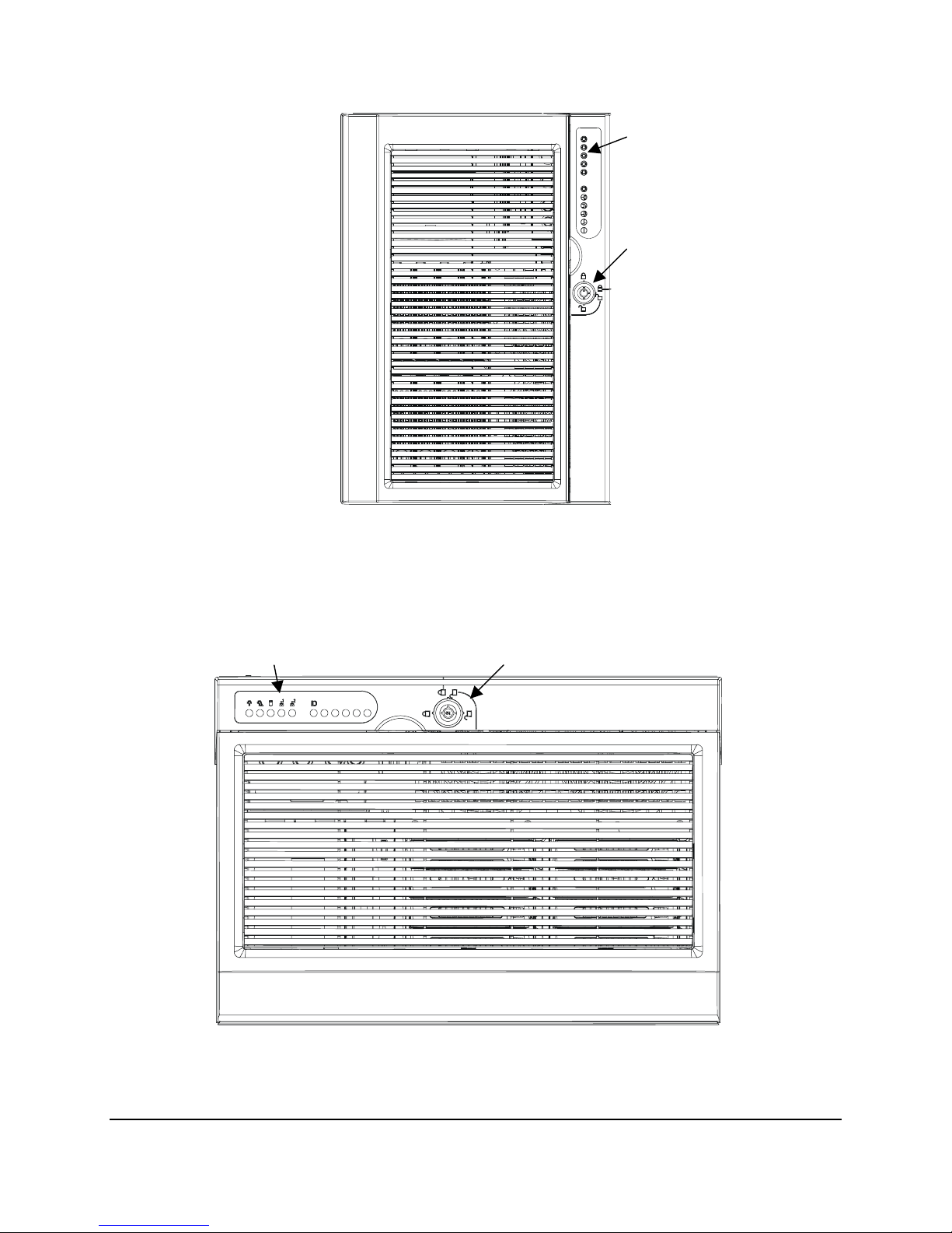
2.1 Front Panel
The front panel contains system control switches and status indicators. Front panel features are
shown in Figure 4 and are described in Table.
Power
LED
Power Button
Fault
LED
HDD
LED
Sleep Button
LAN1
LED
Figure 4: Front Panel Details (Rack Bezel Shown)
LAN2
LED
Reset Button
Chassis
ID LED
Bezel & Top Cover Locked Position
Chassis ID Button
Top Cover Locked &
Bezel Locked
Position
NMI Switch
Bezel & Top Cover
Unlocked Position
Revision 1.11
Intel reference number 10736
5
Page 18
SPSH4 Server Chassis Feature Overview SPSH4 Server System External Product Specification
Table 1 Front Panel Features
Feature Description
Front Panel Button
Reset Resets system power.
Sleep Activates the sleep mode.
NMI (Hidden Behind
Bezel)
Power Toggles system power.
Chassis ID Activates the chassis LED on both the front panel board and on the baseboard at the
Front Panel LEDs
Chassis ID (blue) Indicates that matching chassis ID LED will be present at rear panel of chassis to ease
Power (green) When continuously lit, indicates the presence of DC power in the server. The LED
HDD Activity/Fault
(green/amber)
LAN1 (green) Indicates 100/10Mb Ethernet port activity.
LAN2 (green) Indicates 1000/100/10Mb Ethernet port activity.
System Status/Fault
(green/amber)
Front Panel IO Connectors
USB Connector USB port 3
RJ45 Connector Serial port B.
Causes a non-maskable interrupt. This switch is located behind the front bezel door to
prevent inadvertent activation. The front bezel door must be opened to access this
switch. A narrow tool is required to activate the switch.
rear panel of the chassis.
identification when servicing rear of system in a rack.
goes out when the power is turned off or the power source is disrupted. When flashing
it indicates the system is in ACPI sleep mode.
Indicates any system hard drive activity or fault condition.
Indicates system status or fault condition.
Revision 1.11
6
Page 19
SPSH4 Server SystemTechnical Product Specification
G
R
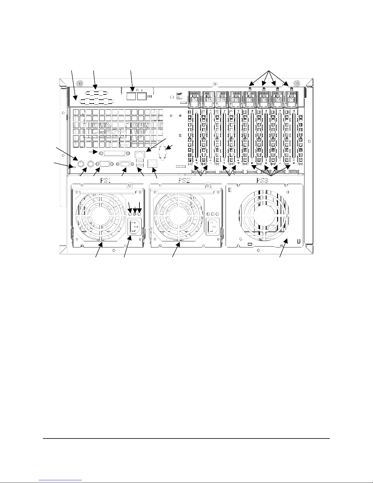
2.2 Rear Features
X
U
B A
C
O
P
D
V W T
SQ
FE
L M N
J K I H
Figure 5: Rear View Of Chassis
Revision 1.11
Intel reference number 10736
7
Page 20

SPSH4 Server Chassis Feature Overview SPSH4 Server System External Product Specification
Table 1: System Features - Rear
Item Description
A Optional External VHDCI SCSI port
B Optional External SCSI3 port
C Optional ICMB connector ports, keyed RJ45 8-pin connector
D Hot Plug PCI-X Power/Fault LEDs
E Two non hot plug 32-bit, 33 MHz PCI add-in card slots
F Two non hot plug 64-bit, 100 MHz PCI-X add-in card slots
G Four hot plug 64-bit, 100 MHz PCI-X add-in card slots
H Filler panel for power bay 3
I Power supply 2
J Power supply IEC320-C14 AC inlet
K Power supply 1
L Power supply on LED (Green)
M Power supply predictive failure LED (Amber)
N Power supply failure LED (Amber)
O LAN1 100/10 RJ45 connector
P Knockout for optional serial port B, 9-pin RS-232 connector
Q LAN2 Gigabit port (1000/100/10)
R USB ports 1 (upper) and 2 (lower), 4-pin connectors
S Video connector
T Serial port A, 9-pin RS-232 connector
U PS/2-compatible parallel port (LPT), 25-pin bi-directional subminiature D connector
V PS/2-compatible mouse port, 6-pin connector
W PS/2-compatible keyboard port, 6-pin connector
X Chassis ID LED (Blue)
Revision 1.11
8
Page 21
SPSH4 Server SystemTechnical Product Specification
3. Physical Specifications
Table 2 describes the physical specifications of the SPSH4 system.
Table 2: Physical Specifications
Specification Black or Beige
Pedestal Value
Height 18.06 inches with feet 7U
Width 12.22 inches Fits 19” standard rack
Depth 25.25 inches 25.25 inches
Clearance Front 3 inches 3 inches
Clearance Rear 4.5 inches 4.5 inches
Clearance Side 0 inches 0 inches
Weight 90 lbs. minumum / 125 lbs.
maximum configuration
Heat Output 3686 BTU/hr (typical) 3686 BTU/hr (typical)
96 lbs. minumum / 125 lb.
Maximum configuration
Rack
Value
Revision 1.11
Intel reference number 10736
9
Page 22
Physical Specifications SPSH4 Server System External Product Specification
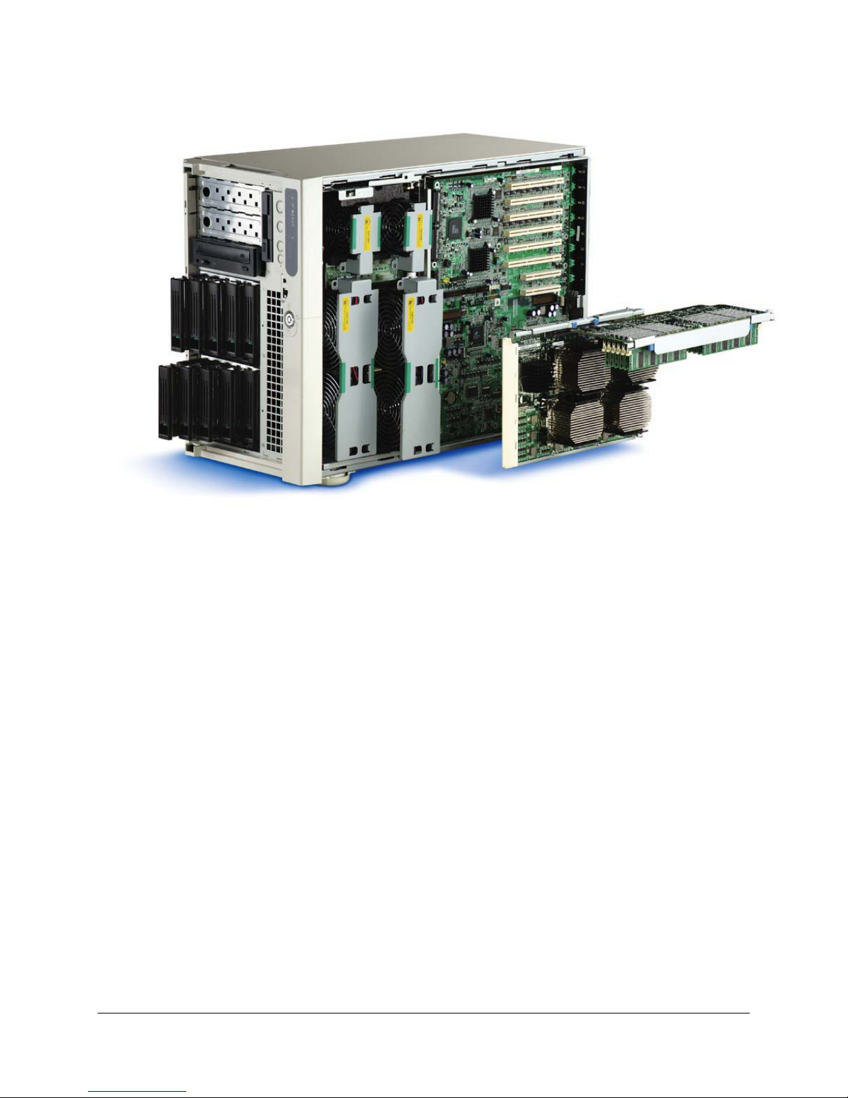
Figure 6: SPSH4 Server System Photograph with Side Panels and Front Panel Removed
Revision 1.11
10
Page 23
SPSH4 Server SystemTechnical Product Specification
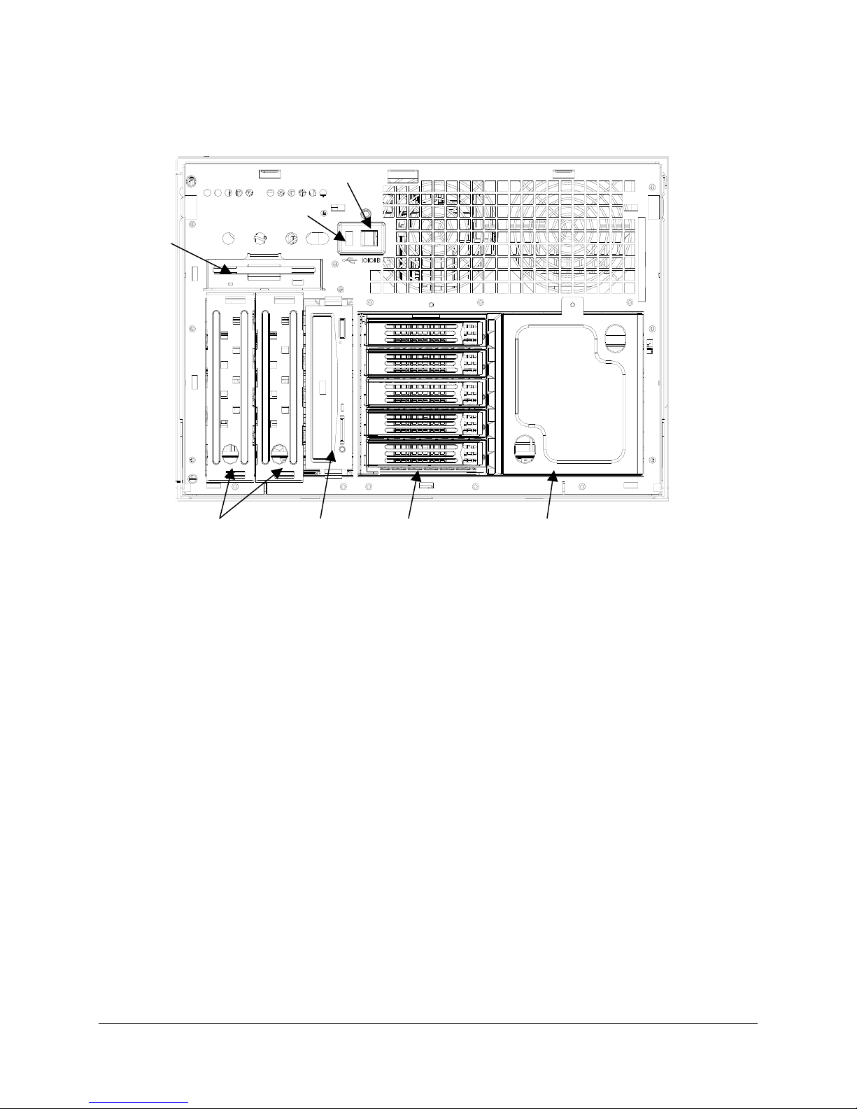
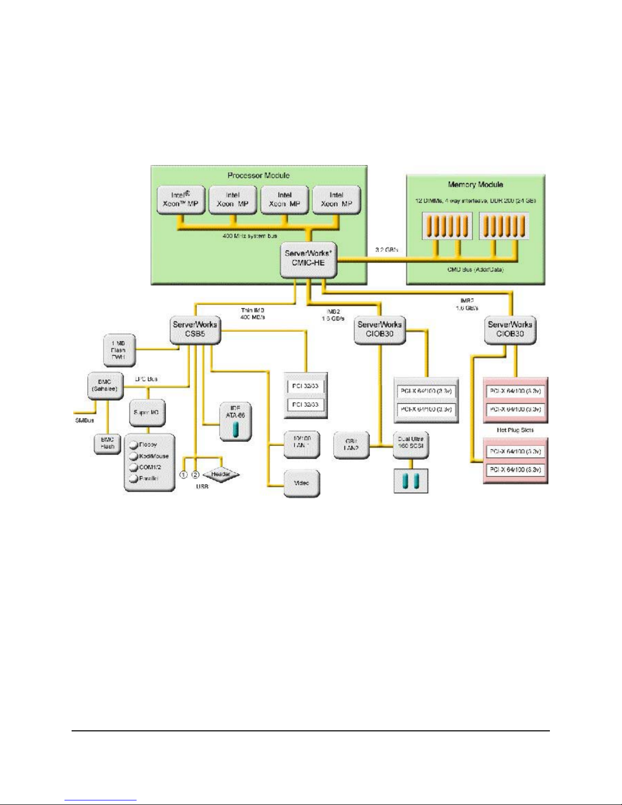
3.1 SSH4 Boardset
This section highlights the main features of the SSH4 baseboard, memory board and processor
board Refer to the SSH4 Baseboard, Processor Board and Memory Module Technical Product
Specification for a detailed description of the SSH4 baseboard.
Figure 7: Functional Block Diagram of SSH4 Boardset
The SSH4 boardset is designed around the Intel® MP Xeon™ processor and the ServerWorks
*
ServerSet* IV Grand Champion High End (GCHE) chipset. This combination provides the basis
for a high performance system with leading edge processor, memory, and I/O performance.
The SSH4 baseboard architecture supports quad processing operation using Intel Intel MP
Xeon processors. It also provides eight industry standard PCI expansion slots supporting a
mixture of 32-bit, 33MHz (two), and 64-bit, 100/66 MHz (six) slots. The baseboard includes an
array of embedded I/O devices, see figure 8 and table 4 below
Revision 1.11
Intel reference number 10736
11
Page 24
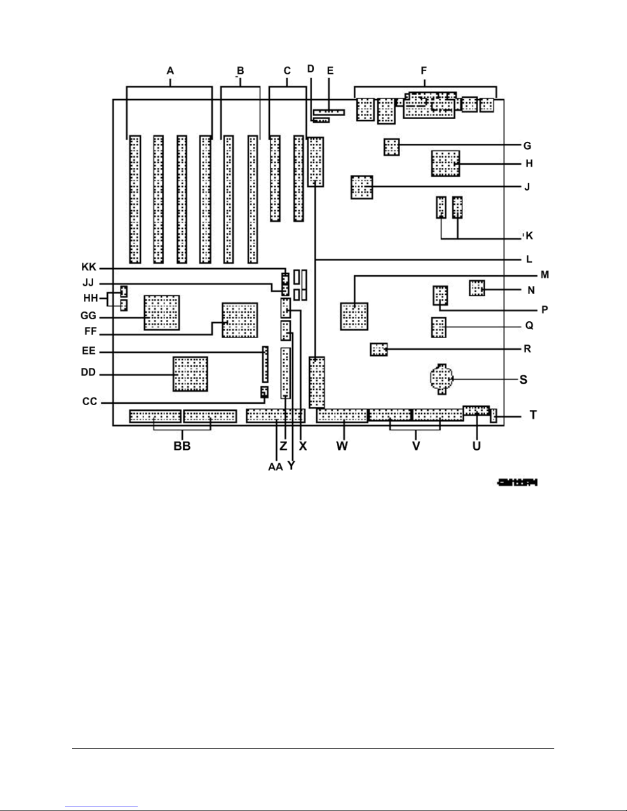
Physical Specifications SPSH4 Server System External Product Specification
Figure 8 SSH4 Baseboard layout
Revision 1.11
12
Page 25
SPSH4 Server SystemTechnical Product Specification
Table 4 SSH4 Baseboard Components
Key Component Key Component
A PCI bus 64 bit, 100 MHz, Hot Plug T Chassis Intrusion Detect connector (P36)
B PCI bus 64 bit, 100 MHz, Non-Hot Plug U 14-pin Power Control connector (P35)
C PCI bus 32 bit, 33 MHz, Non-Hot Plug V 24-pin Power connector (P32)
D ICMB connector (P24) W 20-pin Power connector (P28)
E HPIB connector (P23) X Serial port B connector (P17)
F Back Panel I/O connectors) Y USB #3 Header (P18)
G Intel 82550 Ethernet controller Z Front Panel Header (P19)
H ATI* Rage* XL 2D/3D graphics accelerator AA IDE Connector (P13)
J Intel 82544 Ethernet controller BB SCSI LVD connectors (P4 and P7)
K Video RAM (VRAM) (4 MB total) CC IPMB connector (P12)
L Processor board connectors (P21 and P22) DD AIC7899 or AIC 7902 SCSI controller
M ServerWorks South Bridge Controller (CSB5) EE Fan connector (P11)
N BMC (Sahalee) component FF ServerWorks PCI-X Bus Bridge Controller (CIOB30)
P BIOS Flash component GG ServerWorks PCI-X Bus Bridge Controller (CIOB30)
Q PC87417 Super I/O controller HH RAID LED connectors (P1 and P2)
R BMC Flash component JJ HSBP connector (P16)
S Battery KK HSBP connector (P15)
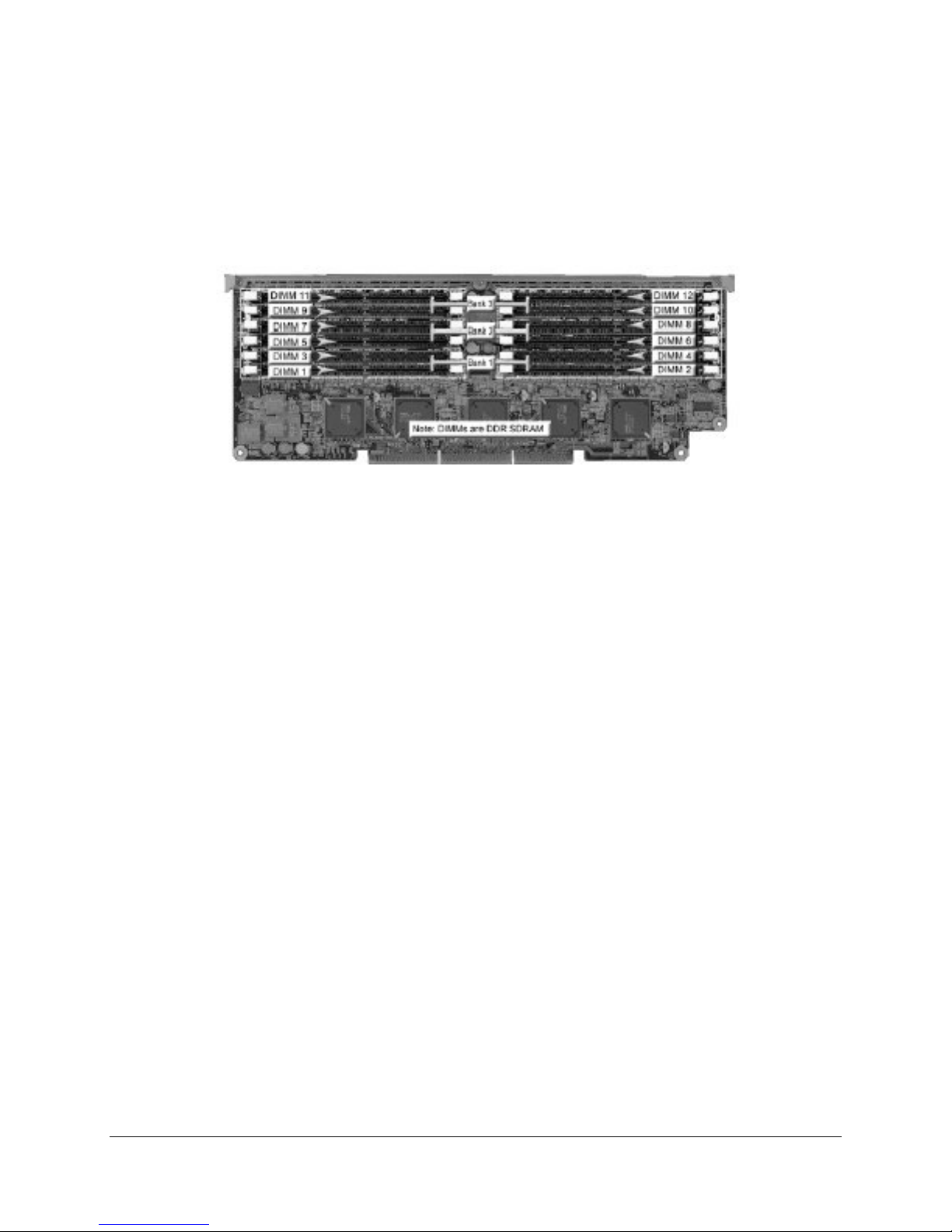
The SSH4 memory subsystem consists of a single memory expansion board. This board
supports up to 12 DDR registered ECC SDRAM memory modules. The SSH4 baseboard
implementation in SPSH4 server supports both stacked and unstacked memory modules for up
to 24 GB of system memory.
The SSH4 boardset provides the following features:
• Three interleaved memory banks.
• Four 184 pin DIMMS per bank.
• Banks must be populated in order.
• Single bit error correction – If a single-bit error is detected, the ECC logic generates a new
Qword with a pattern that corresponds to the originally received 8-bit ECC parity code and
returned to the requestor (the processor or the PCI master)
• Multi Bit error detection – Additional errors within the same Qword constitute a multibit error
which may be unrecoverable. In the case of a multi-bit error, a non-maskable interrupt (NMI)
is issued that instructs the system to shut down to avoid data corruption. ( multibit errors are
very rare ).
• Memory Scrubbing – Error correction is performed on data being read from memory. The
correction is the passed to the requestor and at the same time is “scrubbed” or corrected in
Revision 1.11
Intel reference number 10736
13
Page 26
Physical Specifications SPSH4 Server System External Product Specification
main memory. Memory scrubbing prevents the accumulation of single –bit errors in main
memory tha would become unrecoverable mult-bit errors.
• Chipkill* - Chipkill is the ability of the memory system to wothstand a mult-bit failure within
DRAM device, including a failure that causes incorrect data on all bits of the device.
Figure 9 SSH4 Memory Module
3.2 Guidelines For Installing Memory in the SSH4 Server Board.
• Install only memory modules validated with this particular board. Refer to the Tested
Hardware and Operating System List and/or Http:// support.intel.com.
• Bank 1 must be populated with Dimms first. See figure 9 above.
• All four Dimms within a bank must be identical
• Baseboard Management Controller (BMC) providing monitoring, alerting, and logging of
critical system information obtained from embedded sensors on baseboard
• 8 megabit Flash device for system BIOS
• Three externally accessible USB ports; two at rear bulkhead and one at front panel
• One IDE connector, supporting up to two ATA 66 compatible devices
Revision 1.11
14
Page 27

SPSH4 Server SystemTechnical Product Specification
4. Power supply Subsystem
This section defines the features and functionality of the SSI compliant 600 watt power supply,
a universal input switching power supply. The power supplies are located in the power supply
bay mounted near the rear of the chassis. The system may be configured either with two 600 W
power supplies in a non-redundant configuration, or three 600 W power supplies for a
redundant power (2 + 1) configuration. Each power supply requires an individual power cord.
When the system is configured with three power supplies the following features are supported:
• The user can replace a failed power supply without interrupting system functionality under
any loading condition.
• AC power to one of the power cords can be interrupted without loss of functionality.
Power from the power supply subsystem is carried to internal system boards and peripheral
devices via discrete cables. Two 600 watt power supplies are capable of handling the worst
case power requirements for a fully configured SPSH4 system. This includes four 75 watt Intel
Xeon – MP processors, 24 GB of memory and ten hard drives at 20 watts per drive. Figure 8
shows the SPSH4 power supply.
Revision 1.11
Intel reference number 10736
15
Page 28
Power supply Subsystem SPSH4 Server System External Product Specification
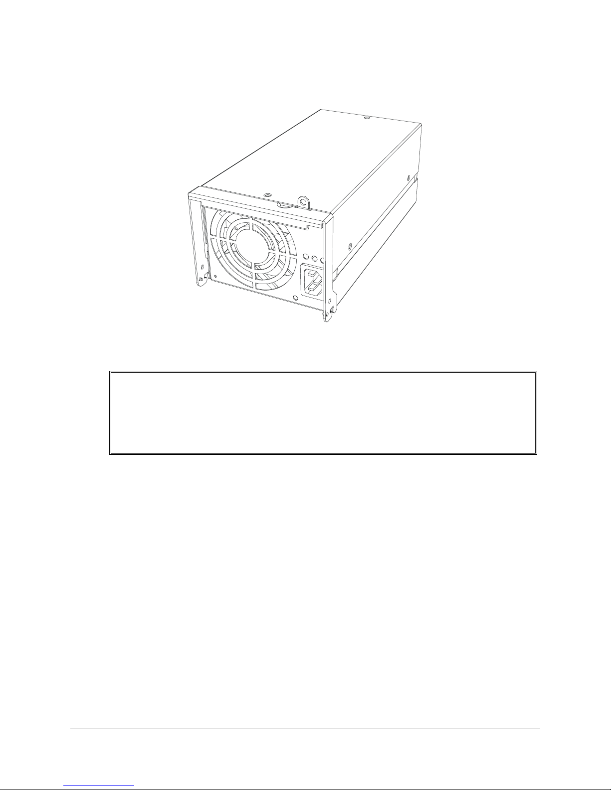
Figure 8: SPSH4 Power supply
!WARNING!
The total power requirement for the SPSH4 server system exceeds the
240VA energy hazard limit that defines an operator accessible area. As a
result, only qualified service personnel should access the processor,
memory, and non-hot plug I/O areas on the system baseboard while the
system is energized.
The following are the main features of the power supply subsystem:
• 1140 W output capability for two or three power supplies in full AC input voltage range
• Up to three 600 watt PFC power factor correcting power supplies for 2+1 power
redundancy
• Power good indication LED
• Predictive failure warning LED
• Failure warning LED
• Internal cooling fans with multi-speed capability
• Remote sense of +3.3V, +5V, and +12V outputs
• AC_OK circuitry for brown out protection
• Built-in load sharing capability
• Built-in overloading protection capability
• On board field replaceable unit (FRU) information for each module
2
C interface for server management functions
• I
Revision 1.11
16
Page 29
SPSH4 Server SystemTechnical Product Specification
• Integral handle for insertion/extraction
• Separate power cords for AC redundancy
The power supplies are populated in the chassis in a specific order as viewed from the rear of
the server system. See Figure 9. For a rack configuration, the power supplies are installed from
left to right. In a pedestal configuration the modules are installed from the bottom to the top. All
of the power supplies implement blind mating connectors for easy installation. Each power
supply implements two AC input fuses rated at 250V/15A, one for line and one neutral. Power
supplies are not required to be on the same AC power phase. The power supply is held to the
chassis frame with four 6-32 screws. These four screws and the AC cord must be removed to
hot swap the power supply.
Figure 9: Rear view of SPSH4 Power Supply Bay
The power supply has four externally enabled outputs: +12V,+5V,+3.3V,-12V, and one +5VSB
(standby) output. The +5VSB standby output is present whenever AC power is applied to any
single power supply. The power supply has a minimum efficiency of 60% to its DC output pins at
maximum load currents at rated nominal input voltages and frequencies.
Several LEDs on each power supply can be viewed from the rear of the server system. These
indicate the power state for that particular module. Looking at the system from rear of the power
supply, from left to right the LEDs are power, predictive fail, and fail.
Revision 1.11
Intel reference number 10736
17
Page 30

Power supply Subsystem SPSH4 Server System External Product Specification
• The power LED is green and blinks to indicate that AC is applied to the power supply and
+5VSB standby output voltage is available. This LED will turn a solid green to indicate the
power supply is on and all the power output voltages are available.
• The predictive fail LED blinks amber LED and indicates the power supply will fail in the near
future due to a poorly performing fan.
• The fail LED is amber and indicates that the power supply has experienced a failure of some
type.
When the power supply configuration changes, the SDR utility must be run so that server
management will properly monitor the new configuration.
A power LED on the front panel, labeled PWR, is green when power is applied to the system.
Table 3 describes the conditions of the LEDs for the power supply.
Table 3: LED Indicators
Power supply LEDs
Power supply Condition Power LED
(green)
No AC power to all PSU OFF OFF OFF
No AC power to this PSU only OFF OFF ON
AC present / Standby Outputs On Blinking OFF OFF
Power supply DC outputs ON and OK ON OFF OFF
Power supply failure OFF OFF ON
Current limit ON OFF Blinking
Predictive failure ON Blinking/Latched OFF
Predictive Fail LED
(amber)
Fail LED
(amber)
4.1 Mechanical Dimensions
Mechanical drawings and dimensions, in millimeters, for the power supply are shown in the
Figure 10 below. The power supply has a handle that pivots to assist insertion and extraction
and provides retention.
Revision 1.11
18
Page 31

SPSH4 Server SystemTechnical Product Specification
Figure 10: SPSH4 Power supply Outline Drawing
Revision 1.11
Intel reference number 10736
19
Page 32

Power supply Subsystem SPSH4 Server System External Product Specification
4.2 Airflow Requirements
Airflow enters the power supply at the DC connector face and is exhausted at the handle face.
Fan speed is controlled by the server system via the FANC signal to the power supply. The
power supply may override the FANC signal and operate the fan at HIGH speed if the
conditions of the power supply exceed those specified in Table 4. The minimum airflow required
by the power supply for high and low intake temperatures are shown in Table 4 also.
Table 4: Airflow Requirements
Item Description Minimum CFM
High Ambient Temperature Airflow through power supply;
max load, T
Low Ambient Temperature Airflow through power supply;
max load, T
=50°C, 5000 ft elevation
intake
=35°C, 5000 ft elevation
intake
4.2.1 Over-Temperature Protection
The power supply is protected against over temperature conditions caused by loss of fan
cooling or excessive ambient temperature. In the event of an OTP condition, the power supply is
shutdown. When the power supply temperature returns to within specified limits, the power
supply will automatically restore power.
21
17
The power supply sends an alert to the system of the OTP condition via the power supply FAIL
signal and the amber FAIL LED at the rear of the failed power supply is illuminated. When
temperatures read by the over temperature sensors in power supply return to within the normal
operating range, DC power is automatically restored. The power supply has built in hysteresis
circuits to prevent the power supply from oscillating on and off due to over temperature recovery
conditions.
4.2.2 Connectors and Pinouts
4.2.2.1 AC Inlet
The power supply AC inlet is an IEC320 C-14 receptacle. The AC power pins and wiring prior to
the protective fuse(s) have a peak current rating higher than the peak inrush current or
maximum fault current drawn by the power subsystem. The safety ground pin of the power
supply is the first pin to connect and the last to disconnect when the AC cord is inserted or
removed from the power subsystem housing.
4.2.2.2 DC Output Connector
The blind-mate DC output connector is the interface to the server system for output voltages,
control signals, and alarm signals. Connector pin descriptions and assignments are listed in
Table 5 and Table 6. Pin A6 is shortened to disabling power supply just prior to disconnecting
the DC output connector during a hot swap operation. The connector is keyed to the power
supply by the positioning of the guide/keying pins on either side of the connector. The keying
location for the connector is A1.
Revision 1.11
20
Page 33

SPSH4 Server SystemTechnical Product Specification
Table 5: Signal Descriptions
Signal Description Signal Description Signal Description
12LS 12V load share bus PWOK
5LS 5V load share bus ACOK
#
Power OK output 5VSB 5V standby output
AC OK output -12 V -12V output
3.3LS 3.3V load share bus ACRange AC input range select SCL I2C Clock signal
12VS 12V remote sense PSKILL Supply fast shutdown SDA I2C Data signal
5VS 5V remote sense FAIL Failure signal A0 I2C address bit 0
3.3VS 3.3V remote sense PRFL Predictive failure signal A1 I2C address bit 1
ReturnS Return remote sense PRESENT
#
PSON
Power enable input
#
Power supply present FANC Fan control signal
Note:
ACOK and AC-Range are reserved for use internal to the power supply.
Table 6: Output Connector Pin-out
Signal Pins
1 2 3 4 5 6
D 12LS PWOK
C A0 SCL FAIL
B A1 SDA 3.3VS 5VS Reserved +5VSB
A 3.3LS PRESENT
P1 P2 P3 P4 P5 P6 P7 P8 P9 P10 P11
+12V +12V GND GND GND GND GND +5 V +5 V +3.3V +3.3V
Notes:
1 The 3.3VSB output is an optional output.
Signals defined as low true use the following convention: signal# = low true
#
#
ACOK
ACRange ReturnS -12 V
PRFL
12VS
FANC 5LS PSON
3.3VSB
#
PSKILL
1
Power Blades
Short Pin
Revision 1.11
Intel reference number 10736
Figure 11: Connector Pin Locations
21
Page 34

Power supply Subsystem SPSH4 Server System External Product Specification
4.2.3 AC Electrical Specifications
4.2.3.1 AC / DC Supply Redundancy
The power sub-system has three AC inlets, one for each power supply. Each power supply
does not rely on other modules for any functionality except for load sharing. AC input to the
power supply is fully isolated. Therefore, it is not subject to AC phase differential issues. All DC
outputs have a device to isolate the power supply from the main system power during a power
supply failure or during a hot swap operation. The SPSH4 server system has power redundancy
for any DC load condition in a 2+1 power supply configuration.
4.2.3.2 AC Input Voltage Ranges
The power supply incorporates universal power input with active power factor correction, which
reduces line harmonics in accordance with the EN61000-3-2 and JEIDA MITI standards. The
power supply operates within all specified limits over the input voltage range specified in Table
7. Harmonic distortion of up to 10% THD will not cause the power supply to go out of specified
limits. The power supply has a minimum efficiency of 60% to the DC output pins at maximum
load currents, at rated nominal input voltages and frequencies.
Table 7: AC Input Voltage Rating
Parameter Minimum Rated Maximum Max Input Current
(600W)
Voltage (110) 90 V
Voltage (220) 180 V
Frequency 47 Hz 50/60 Hz 63 Hz -
100-127 V
rms
200-240 V
rms
132 V
rms
264 V
rms
12 A
rms
6 A
rms
rms
rms
4.2.3.3 AC Line Dropout and Hold-up Time
An AC line dropout is defined as when the AC input drops to 0VAC for one cycle or less during
any phase of the AC line. During an AC dropout, the power supply meets the dynamic voltage
regulation requirements over the rated load. Dynamic voltage regulation requirements may be
seen in Table 20.
An AC line dropout will not cause any tripping of control signals or protection circuits. If the AC
dropout lasts longer than one cycle then the power supply may shutdown but will recover and
meet all turn on requirements. The power supply meets the AC dropout requirements over all
rated AC voltages, frequencies, and output loading conditions. Any dropout of the AC line will
not cause damage to the power supply.
4.2.3.4 AC Line Transient Specification
AC line transient conditions are defined as “sag” and “surge” conditions. The sag conditions are
also commonly referred to as “brownout”. The sag condition is defined as the AC line voltage
dropping below nominal voltage. The surge conditions are defined as when the AC line voltage
rises above nominal voltage. The power supply meets the performance requirements under the
AC line sag and surge conditions shown in Table 8 and Table 9, respectively.
Revision 1.11
22
Page 35

SPSH4 Server SystemTechnical Product Specification
Table 8: AC Line Sag Transient Performance
Duration Sag Operating AC Voltage Line
Continuous 10% 100VAC-127VAC
200VAC-240VAC
0 to 1 AC cycle 100% 100VAC-127VAC
200VAC-240VAC
> 1 AC cycle >10% No loss of function or
performance
50/60Hz No loss of function or performance
50/60Hz No loss of function or performance
50/60Hz Loss of function acceptable,
Frequency
Performance Criteria
self recoverable
Table 9: AC Line Surge Transient Performance
Duration Surge Operating AC Voltage Line
Frequency
Continuous 10% 100VAC-120VAC
200VAC-240VAC
0 to ½ cycle 30% 110VAC, 220VAC 50/60Hz No loss of function or performance.
50/60Hz No loss of function or performance.
Performance Criteria
4.2.3.5 Susceptibility
The power supply complies with the limits defined in EN50082-2 while maintaining normal
performance within the specification limits.
Table 10: Electrostatic Discharge, IEC 801-2/IEC 1000-4-2
Level Test Voltage, Contact
Discharge
3 8Kv 15Kv
Test Voltage, Air
Discharge
Table 11: Electrical Fast Transient/Burst, IEC 801-4/IEC 1000-4-4
Level AC Inlet
3 1Kv
Table 12: Radiated Immunity, IEC 801-3/IEC1000-4-3
Field Strength Frequency Range Step Size Modulation
5V/meter 26MHz to 500MHz 1% of previous frequency None
4.2.3.6 Surge Immunity
In addition to complying with EN50082-2 for Surge immunity, the product must also comply with
ANSI C62.45-1992. The requirements of the Intel Environmental & Reliability Board and System
Revision 1.11
Intel reference number 10736
23
Page 36

Power supply Subsystem SPSH4 Server System External Product Specification
Validation Test Handbook for surge withstand capability indicates the test methods and levels
used during Intel system qualification testing, which are derived from these standards.
Table 13: Surge Immunity IEC 1000-4-5
Level Open Circuit
Voltage
3
2.0Kv ± 10%
Minimum time between
Surges
20 sec
Table 14: Ring Wave
Open Circuit
Voltage
3.0Kv ± 10%
Minimum time between
Surges
20 sec
4.2.3.7 AC Line Fast Transient Response
The power supply meets the EN61000-4-5 directive and any additional requirements in
IEC1000-4-5: 1995 and the Level 3 requirements for surge-withstand capability.
Revision 1.11
24
Page 37

SPSH4 Server SystemTechnical Product Specification
4.2.3.8 AC Line Inrush
AC line inrush current does not exceed 25A peak for quarter of the AC cycle. The inrush current
must not exceed the I
2
t curve shown in Figure 12. The inrush current must not exceed 100A
peak for any duration of time.
The power supply meets the inrush requirements for any rated AC voltage, during turn on at any
phase of AC voltage, during hot plug, during any AC dropout condition, over the specified
temperature range, and during AC power cycling.
120
100
80
60
amps
40
20
0
0 5 10 15 20
ms ec
Figure 12: Inrush Curve
4.2.3.9 Dielectric Strength Requirements
The power supply meets all safety agency requirements for dielectric strength.
4.2.3.10 AC Line Fuse
Each power supply has two line fuses, one for each side of the AC input. AC line-fusing meets
all safety agency requirements.
4.2.3.11 AC Inlet Connector
The AC input connector is an IEC 320 C-14 power inlet. This inlet is rated for 15A / 250VAC.
4.2.4 DC Output Specification
The SPSH4 server system runs with either two or three power supplys installed. The power
supplys operate with their outputs directly paralleled. The power supplys equally share the total
load currents within the limits specified. Equal power sharing of paralleled power supplys is
required to prevent life shortening stress concentration in individual power supplys. Power
sharing is accomplished by actively matching the output currents on the high power outputs.
The current sharing load deviation is defined as follows:
Load_Deviation = [(Actual_Load – Mean_ Load)/(Mean Load)] * 100%
Revision 1.11
Intel reference number 10736
25
Page 38

Power supply Subsystem SPSH4 Server System External Product Specification
Steady state DC output voltages at the remote sense points always remain within the limits
specified by Table 15 for all combinations of operating line, load, load transient, and
environment specified herein.
Table 15: DC Output Voltage Limits
Parameter Minimum Nominal Maximum Units Tolerance
+3.3V + 3.25 + 3.30 + 3.35 V
+5V + 4.90 +5.00 + 5.10 V
+12V + 11.76 +12.00 + 12.24 V
-12V - 13.08 -12.00 - 11.40 V + 9% and -5%
+5V Standby1 + 4.85 +5.00 + 5.20 V + 4% and -3%
Note:
1 +5V standby is in reference to the common remote sense returning potential.
± 1.5%
± 2%
± 2%
Revision 1.11
26
Page 39

SPSH4 Server SystemTechnical Product Specification
4.2.4.1 DC Output Rating
The power supply meets the static regulation requirements under the loading conditions
specified in Table 16. The combined continuous output load applied to the power supply will not
exceed 600 W. If the power exceeds 600 W, the power supply should not be subjected to this
maximum current draw for more than 12 seconds.
Table 16: 600W Load Ratings
Voltage
+3.3V 1 A 40 A
+5V 1 A 34 A
+12V 0 A 36 A 42 A
-12V 0 A 1.0 A
+5V Standby 0 A 2 A
Minimum Continuous Maximum Continuous Peak
Single Power supply Maximum Output Current
The total system maximum load condition is shown in Table 17. Either two or three power
supplys can support the total system maximum load.
Table 17: Total System Load at Line AC Input
Total System Maximum Load Condition
Voltage Minimum Continuous Maximum Continuous Peak
+3.3V 1.5 A 76 A
+5V 1.5 A 64.6 A
+12V 1.5 A 68.4 A 79.8A
-12V 0.0 A 1.0 A
+5V Standby 0.0 A 2.0 A
Table 18: Absolute Worst Case System Power Budget
Subsystem Qty +5V +3.3V +12V -12V +5VSB Total (W)
Board Set 1 4.36 10.76 1.15 0.01 0.38 73.13
CPU 4 30.85 370.20
DDR DRAM 12 1.97 6.10 79.70
FAN 6 6.32 75.84
HDD 10 11.00 9.00 163.00
CD-ROM 1 0.40 0.70 10.40
FDD 1 0.24 1.20
5½" Device 2 1.54 0.80 17.30
PCI-X (64bit/100MHz) 6 9.00 13.64 0.31 91.56
Revision 1.11
Intel reference number 10736
27
Page 40

Power supply Subsystem SPSH4 Server System External Product Specification
Subsystem Qty +5V +3.3V +12V -12V +5VSB Total (W)
PCI (32bit/33MHz) 2 6.00 0.03 30.15
System Total 32.54 26.37 54.92 0.01 0.72 912.48
Power Subsystem Spec 64.60 76.00 68.40 1.00 2.00 1140.00
Margin 32.06 49.63 13.48 0.99 1.28 227.52
4.2.4.2 Remote Sense
The power supply has remote sense return (ReturnS) to regulate out ground drops for all output
voltages (+3.3V, +5V, +12V, -12V and +5VSB). The power supply operates within the
specification shown in Table 19 over the full range of voltage drops from the power supply’s
output connector to the remote sense points on the server system boardset.
Table 19: Remote Sense Drops
Output Max Drops Units
+3.3V 250 mV
+5V 250 mV
+12V 500 mV
Remote Sense return 100 mV
4.2.4.3 DC and Transient Load Output Voltage Limit
The power supply will maintain regulation specified in Table 20 under all specified conditions,
including parallel operation with other power supplys, line variations, load variations, transient
load conditions, peak ripple/noise, maximum remote sense drops, subsystem hot swap, and
temperature change. The +3.3V, +5V, and +12V output voltages should be measured at their
respective remote sense points. The output voltages must stay within regulation requirements
with the remote sense regulating out the maximum drops shown in Table 19.
Table 20: Dynamic Tolerance Requirement
Output Min. Output [V] Max. Output [V] Tolerance
+3.3V 3.20 3.43 +4% & -3 %
+5V 4.85 5.20 +4% & -3 %
-12V 11.4 13.08 +9 & -5%
+12V 11.64 12.48 +4% & -3 %
+5V standby 4.85 5.20 +4% & -3 %
Revision 1.11
28
Page 41

SPSH4 Server SystemTechnical Product Specification
D
4.2.4.4 Ripple and Noise
The maximum allowed ripple/noise output of the power supply is defined in Table 21. This is
measured over a bandwidth of 0Hz to 20MHz at the power supply output connector. A 10µF
tantalum capacitor in parallel with a 0.1µF ceramic capacitor are placed at the point of
measurement. The test setup is shown in Figure 13.
V
OUT
AC
Earth GND
POWER SUPPLY
V
RETURN
GENERAL NOTES:
1. LOAD THE OUTPUT WITH ITS MINIMUM
LOAD CURRENT.
2. CONNECT THE PROBES AS SHOWN.
3. REPEAT THE MEASUREMENTS WITH THE
MAXIMUM LOAD ON THE OUTPUT.
SCOPE NOTE:
USE A TEKTRONIX 7834 OSCILLOSCOPE WITH 7A13 AN
P6055 PROBES OR EQUIVALENT.
Figure 13: Differential Noise Test Setup
Table 21: Ripple and Noise
LOAD
10uF
(low ESR)
SCOPE
Voltage Ripple / Noise pk-pk Ripple/Noise pk-pk
+3.3V 1.5% 50 mV
+5V 1% 50 mV
+12V 1% 120 mV
-12V 1% 120 mV
+5V Standby 1% 50 mV
Revision 1.11
Intel reference number 10736
29
Page 42

Power supply Subsystem SPSH4 Server System External Product Specification
4.2.4.5 Power Timing
Power timing refers to the timing requirements for single power supply operation. The output
voltages must rise from 10% to within regulation limits (T
) within 5 to 200ms. The +3.3V,
vout_rise
+5V and +12V output voltages should start to rise approximately at the same time. All outputs
must rise monotonically. The +5V output needs to be greater than the +3.3V output during any
point of the voltage rise, however, never by more than 2.25V.
Each output voltage reaches regulation within 100ms (T
off within 100ms (T
power supply being turned on and off via the AC input, with PSON held low and the PSON
signal, with the AC input applied. The ACOK
) of each other. Figure 14 shows the timing requirements for a single
vout_on
#
signal is not being used to enable the turn on
) of each other and begin to turn
vout_on
timing of the power supply.
Table 22: Output Voltage Timing
Item Description Min Max Units
T
Output voltage rise time from each main output. 5 200 msec
vout_rise
T
All main outputs must be within regulation of each other within this time. 300 msec
vout_off
T
All main outputs must be within regulation of each other within this time. 100 msec
vout_on
10% Vout
T
T
vout rise
T
vout_off
Figure 14: Output Voltage Timing
Table 23: Turn On/Off Timing
Revision 1.11
30
Page 43

SPSH4 Server SystemTechnical Product Specification
_
Item Description Min Max Units
T
sb_on_delay
T
ac_on_delay
T
vout_holdup
T
pwok_holdup
T
pson_on_delay
T
pson_pwok
T
acok_delay
T
pwok_on
T
pwok_off
T
pwok_low
T
sb_vout
Delay from AC being applied to 5VSB being within regulation. 1500 msec
Delay from AC being applied to all output voltages being within regulation. 2500 msec
Time all output voltages, including 5VSB, stay within regulation after loss of
21 msec
AC.
Delay from loss of AC to deassertion of PWOK
20 msec
Delay from PSON# active to output voltages within regulation limits. 5 400 Msec
Delay from PSON# deactive to PWOK being deasserted. 50 Msec
Delay from loss of AC input to deassertion of ACOK#. 20 Msec
Delay from output voltages within regulation limits to PWOK asserted at
100 1000 Msec
turn on.
Delay from PWOK deasserted to output voltages (3.3V, 5V, 12V, -12V,
1 Msec
5VSB) dropping out of regulation limits.
Duration of PWOK being in the deasserted state during an off/on cycle
100 Msec
using AC or the PSON signal.
Delay from 5VSB being in regulation to 5V being in regulation at AC turn
50 1000 Msec
on.
AC Input
Vout
PWOK
5VSB
PSON
ACOK#
T
sb_on_delay
T
vout_holdup
T
T
AC_on_delay
T
T
pwok_holdup
T
acok_delay
pwok_off
T
sb
vout
AC turn on/off cycle
T
pwok_on
pwok_low
T
sb_on_delay
T
pwok_on
T
pson_on_delay
PSON turn on/off cycle
T
pwok_off
T
pson_pwok
T
pson_off_delay
Revision 1.11
Intel reference number 10736
Figure 15: Turn On/Off Timing
31
Page 44

Power supply Subsystem SPSH4 Server System External Product Specification
4.2.5 Electrical Protection Circuits
Protection circuits inside the power supply will cause only the power supply’s main outputs to
shutdown during either an over-voltage or over-current condition. The 5VSB output remains
powered on if the failure does not involve this output. When a protection circuit shuts down the
power supply, both the FAIL LED and the FAIL signal will be activated.
4.2.5.1 Over-Voltage Protection
Over-voltage protection is sensed inside the power supply. The power supply will shutdown and
latch off following an over-voltage condition. This latch can be cleared by toggling the power
supply PSON
limit applies to all specified AC input voltages and output load conditions. Table 24 contains the
over-voltage limits. The values are measured at the output of the power supply DC connector.
#
signal or by an AC power interruption of greater than 1 second. This over-voltage
Table 24: Over-Voltage Limits
Output Voltage Protection Point [ V]
+3.3 V 3.8 – 4.5
+5 V 5.6 – 6.5
+12 V 13 – 14.5
4.2.5.2 Over- Current Protection
The power supply has over-current protection on +3.3V, +5V, and +12V outputs. The current
limiting is of the voltage fold-back type. The over-current limit levels specified in Table 25 are
maintained for a period of 2.6-second minimum and 3.6-second maximum. After this time the
power supply will latch off. The power supply cannot be damaged from repeated power cycling
in this condition.
Table 25: Over Current Protection Limits
Voltage Over-current Limit
+3.3V 44.0 A minimum; 60.0 A maximum
+5V 37.4 A minimum; 51.0 A maximum
+12V 39.6 A minimum; 54.0 A maximum
Note:
Limits specified are per 600W power supply.
Revision 1.11
32
Page 45

SPSH4 Server SystemTechnical Product Specification
4.2.6 Control Signals
4.2.6.1 PSON
The PSON
signal that turns on the 3.3V, 5V, 12V, and -12V power rails. When this signal is not pulled low
by the system, or if it is left open, the outputs (except the 5VSB) turn off. This signal is pulled to
a standby voltage by a pull-up resistor internal to the power supply. See Figure 15 for the timing
diagram.
#
signal is required to remotely turn on/off the power supply. PSON# is an active low
Table 26: PSON Signal Characteristic
Signal Type Accepts an open collector/drain input from the
system. Pull-up to VSB located in power supply.
PSON# = Low, PSKILL = Low
PSON# = Open, PSKILL = Low or Open
PSON# = Low, PSKILL = Open
Logic level low (power supply ON)
Logic level high (power supply OFF)
Source current, Vpson = low
Power up delay: T
Power down delay: T
PWOK delay: T
pson_on_delay
pson_off_delay
pson_pwok
ON
OFF
OFF
MIN MAX
0V 1.0V
2.0V 5.25V
4ma
5msec 400msec
1.1msec
50msec
4.2.6.2 PWOK
PWOK is a power good signal and will be pulled HIGH by the power supply to indicate that all
the outputs are within the regulation limits of the power supply. When any output voltage falls
below regulation limits or when AC power has been removed for a time sufficiently long so that
power supply operation is no longer guaranteed, PWOK will be de-asserted to a LOW state.
See Figure 15 for a representation of the timing characteristics of PWOK. The start of the
PWOK delay time is inhibited as long as any power supply output is in current limit.
Table 27: PWOK Signal Characteristics
Signal Type Open collector/drain output from power supply.
Pull-up to VSB located power supply.
PWOK = High
PWOK = Low
Logic level low voltage, Isink=4mA
Logic level high voltage, Isource=200µA
Sink current, PWOK = low
Source current, PWOK = high
PWOK delay: T
PWOK rise and fall time
Power down delay: T
pwok_on
pwok_off
Power Good
Power Not Good
MIN MAX
0V 0.4V
2.4V 5.25V
4mA
2mA
100ms 1000ms
1ms 200mSec
100µsec
Revision 1.11
Intel reference number 10736
33
Page 46

Power supply Subsystem SPSH4 Server System External Product Specification
4.2.6.3 PSKILL Signal
The PSKILL pin allows for hot swapping of the power supply. The PSKILL pin on the power
supply is shorter than the other signal pins. When a power supply is operating in parallel with
other power supplys and then extracted from the system, the PSKILL pin will quickly turn off the
power supply and prevent arching of the DC output contacts. T
(shown in Table 28) is the
PSKILL
minimum time delay from when PSKILL pin unmates to when the power supply shuts down all
power outputs.
When the PSKILL signal pin is not pulled down or left opened (for example when the power
supply is being extracting from the system), the power supply will shut down regardless of the
condition of the PSON
#
signal. The mating pin of this signal in the system is tied to ground.
Internal to the power supply, the PSKILL pin is connected to a standby voltage through a pull-up
resistor. Upon receiving a LOW state signal at the PSKill pin, the power supply will be allowed to
turn on via the PSON
Signal Type (Input Signal to Supply) Accepts a ground input from the system. Pull-up to
PSKILL = Low, PSON# = Low
PSKILL = Open, PSON# = Low or Open
PSKILL = Low, PSON# = Open
Logic level low (power supply ON)
Logic level high (power supply OFF)
Source current, Vpskill = low
Delay from PSKILL=High to power supply
Note:
T
is the time from the PSKill signal deasserting HIGH to the power supply’s output inductor
PSKill
#
signal. Logic LOW on this pin by itself will not turn on the power outputs.
turned off (T
Table 28: PSKILL Signal Characteristics
VSB located in the power supply.
ON
OFF
OFF
MIN MAX
0V 1.0V
2.0V 5.25V
4ma
)1
PSKill
100µsec
Revision 1.11
34
Page 47

SPSH4 Server SystemTechnical Product Specification
4.2.6.4 Power supply Failure
In the event of a power supply failure (OVP at any output, UV at any output, fan failure, or other
failure) the power supply failure signal is allowed to go HIGH by the power supply.
Table 29: FAIL Signal Characteristics
Signal Type Open collector/drain output from power supply. Pull-
up to VSB located system.
FAIL = High
FAIL = Low
Logic level low voltage, Isink=4ma
Logic level high voltage, Isink=50µA
Sink current, FAIL = low
Sink current, FAIL = high
FAIL rise and fall time
Failed
OK
MIN MAX
0V 0.4V
5.25V
4ma
50µA
100µsec
4.2.6.5 Predictive Failure Signal
This signal indicates that the power supply (or power supply fan) is reaching its end of life. The
signal indicates a predictive failure when HIGH.
Table 30: PRFL Signal Characteristics
Signal Type (Active Low) Open collector/drain output from power supply. Pull-
up to VSB located in system.
PRFL = High
PRFL = Low
Logic level low voltage, Isink=4mA
Logic level high voltage, Isink=50µA
Sink current, FAIL = low
Sink current, FAIL = high
PRFL rise and fall time
Failing
OK
MIN MAX
0V 0.4V
5.25V
4mA
50µA
100µsec
Revision 1.11
Intel reference number 10736
35
Page 48

Power supply Subsystem SPSH4 Server System External Product Specification
4.2.6.6 Power supply Present Indicator
The PRESENT
#
signal is used to sense the number of power supplys in the system (operational
or not). This signal is connected to the power supply’s output ground.
Table 31: PRESENT# Signal Characteristics
Signal Type Output from power supply that is connected to ground.
Pull-up to VSB located in system.
PRESENT# = Low
PRESENT# = High
Logic level low voltage, Isink=4mA
Logic level high voltage, Isink=50µA
Sink current, PRESENT# = low
Sink current, PRESENT# = high
Present
Not Present
MIN MAX
0V 0.4V
5.25V
4mA
50µA
4.2.6.7 Power supply Fan Control
The power supply fan speed is controlled by the FANC signal. The fan speed (even during sleep
mode) is controlled by a variable voltage on this pin. This signal allows the system to request
control of the power supply fan. The control circuit in the system supplies voltage to this pin
from 12V to 0V for the fan control request. If the FANC signal is left open the fan control
defaults to power supply control.
Table 32: Fan Speed Control
Signal Type Accepts an input voltage from the system. Pull-up to
12V located in power supply.
FANC < 1V
2V < FANC < 3V
3V < FANC < 10.5V
FANC > 10.5V
Source current
Fan SLEEP mode output power 2
Fan LOW speed ambient temperature
Notes
1. This is a request from the system to the power supply to operate the fan at this condition. The power supply
can over ride this request and increase the fan speed if the power supply requires more cooling. See note 2
for fan SLEEP mode requirements.
2. When the power supply fan is in SLEEP mode the fan must be operating at its minimum RPM, which is slow
enough to not output any noticeable audible levels. The power supply must be able to supply 0W to 50W of
output power at 50°C ambient (any combinations of 3.3V, 5V, and 12V output currents) in the power supply
fan SLEEP mode condition without the power supply over riding and turning the fan to LOW or HIGH speed.
Fan in SLEEP mode
Fan in LOW speed
Fan ramps from LOW to HIGH speed 1
Fan in HIGH speed
MIN MAX
2mA
50W
1
1
1
35°C
Revision 1.11
36
Page 49

SPSH4 Server SystemTechnical Product Specification
4.2.6.8 Power supply Field Replacement Unit (FRU) Signals
The FRU data format is compliant with the Intelligent Platform Management Interface (IPMI)
Specification 1.5. The current version of these specifications is available at
http://developer.intel.com/design/servers/ipmi/spec.htm
Four pins are allocated for the FRU information on the power supply connector. One pin is the
Serial Clock (SCL). The second pin is used for Serial Data (SDA). Pins three and four are
address lines A0 and A1 to indicate to the power supply’s EEPROM which position the power
supply is located in the server system.
Table 33: Pins for Power supply Connector FRU Information
A0 A1 Address
Low Low 0xA0
Low High 0xA2
High Low 0xA5
High High 0xA6
The FRU circuits inside the power supply are powered off of 5VSB on the system side of the
or’ing device and grounded to ReturnS (remote sense return). The Write Control (or Write
protect) pin is tied to ReturnS inside the power supply so that server management can write to
the EEPROM.
Revision 1.11
Intel reference number 10736
37
Page 50

Power supply Subsystem SPSH4 Server System External Product Specification
4.3 Cooling Subsystem
Main system components are cooled by a set of fans mounted in a fan bay near the front of the
chassis and in front of the E-bay. The fan bay is shown below.
120mm Fan
Banks
Figure 16: Fan Bay (Shown with all Fan Banks Installed)
80mm
Fans
Fan
Board
The SPSH4 system comes in a redundant four-fan bank configuration consisting of two 120mm
fan banks for cooling the processor section of E-bay and two 80mm fan for cooling PCI section
of E-bay. The fans blind mate connect to the system fan board. Only a minimal configuration is
supported in the two fan bank configuration (one 120mm fan bank plus one 80mm fan):
• One processor
• Four memory DIMMs
Note: Since SCSI bay hard drives and 5
¼” peripheral bays are not cooled by dedicated SCSI
bay fans and from power supply fans, they are not subject to any limitations from the two-fan
bank configuration described above.
The four-fan bank configuration supports any system configuration. Air flows through the fan
bay and then through E-bay, and exhausts through the rear panel of the system. Additionally,
both SCSI bay fans and power supply fans pull air from the SCSI bays and from the 5
¼“
peripheral bay. Each fan provides tachometer signal output to server management to indicate a
fan failure. Each fan also provides a presence signal to the fan board to indicate a missing fan.
4.3.1 Redundancy and Ambient Temperature Control
The fan board contains a pulse-width-modulation (PWM) circuit, which cycles the +12 V fan
voltage to provide quiet operation when system ambient temperature is low, and there are no
fan failures. Under normal room ambient conditions (less than 30°C) the fan power control
Revision 1.11
38
Page 51

SPSH4 Server SystemTechnical Product Specification
circuit operates the fans at low speed. When ambient temperature is between 30°C and 35°C or
a fan fails, the fan power control circuit operates the fans at maximum speed.
4.3.2 Cooling Summary
The redundant, six fan cooling subsystem is sized to provide cooling for:
• Up to four Intel MP Xeon processors dissipating 75 W each
• 24 GB of DDR memory
• Ten 15k RPM hard drives
• Eight full-length PCI cards
• Three 5
• DC output redundant, fully-loaded power subsystem
The cooling subsystem is designed using a worst-case analysis with no margin under a single
fan failure condition. The lower fan speed settings were chosen to meet acoustic and thermal
requirements. To ensure that all components remain within specification under all system
environmental conditions, there will be a recommended time limit for fan and power supply
module hot-swap operations.
¼“ peripheral bay devices
Revision 1.11
Intel reference number 10736
39
Page 52

Cables and Connectors SPSH4 Server System External Product Specification
5. Cables and Connectors
This chapter describes interconnections between the various components of the SPSH4
system. This chapter includes an overview diagram of the SPSH4 server system
interconnections. Refer to the appropriate board External Product Specification for other
connector signal descriptions and pin-outs.
5.1 Interconnect Block Diagram
Figure 17 shows interconnections for all of the boards used in the SPSH4 server system.
1 2 43 5
SAF-TE
Board
1x4 Pin Pwr CBL
Three 4x6pin+11power blade
connectors to power supplies
600 W
PS 1
External Power Cord
2x2 Pin Pwr CBL
2x5 Internal Serial Cable
PDB
600 W
PS 2
External Power Cord
External Power Cord
2x5 Internal USB cable
120 Pin Edge
92mm
Fan
2x7 Pin Pwr CBL
600 W
PS 3
(Optio nal)
(Drives Optional)
80 Pin SCA2 Connectors
Secondary 1"x5
HDD Backplane
(Optional)
Connector
FAN 1 FAN 1
1x4 Pin I2C CBL
2x20 Pin Pwr CBL
External Power Cord
2x - 2x5 Pin Fan Connections (120mm Fans Banks)
2x - 2x2 Pin Fan Connectors (80mm Fans)
120mm
Fan Bank
Baseboard
Processor Module - 4 Foster ZIF Sockets
603 Pin
4
2x24 Pin Pwr CBL
3
LAN1 (100/10), LAN2 (1000/100/10), Video, 1
Serial A (Plus 1 Serial B Knockout), 1 Parallel,
Keyboard, Mouse,2 USB (All External Interfaces)
Fan PCB -
120mm
Fan Bank
Pwr 1Aux
1
2
SAF-TE
Board
1x4 Pin Pwr CBL
80mm
Fan
Pwr 2
Memoy Module - 12
DIMMs 168Pin Each
5 Pin CBL
(Optional)
ICMB Board (Optional
External Interface)
Slot 2 - 330 Pin
1x5 ICMB
Conn
(Drives Optional)
1 2 43 5
80 Pin SCA2 Connectors
Primary 1"x5
HDD Backplane
Connector
120 Pin Edge
92mm
Fan
80mm
Fan
2x20 Pin IDE CBL
2x17 Pin Floppy CBL
IDEFloppy
FP
HDM 144 Pin
HDM 144 Pin
HPIB Conn
HPIB PBA (External Interface)
USB
Serial
I2C B I2C A
32/33 PCI
2x14 Pin CBL
1"
5.25"
Device
Wide SCSI
Conn 68 Pin
64/100/66 PCI
Wide SCSI3 Port
(Optional External
Interface)
Floppy
SCSI CBL (Optional)
68 Pin Wide U-160 5.25"
68 Pin Wide U-160 SCSI CBL
64/100/66 PCI
Front
Panel
5.25"
5.25"
IDE
Device
CDROM
2x17 Pin CBL
1x4 Pin Pwr CBL
1x4 Pin I2C CBL
2x17 Pin Fan CBL
68 Pin Wide U-160 SCSI CBL
Wide SCSI
Conn 68 Pin
Fan
64/100/66 PCI
64/100/66 PCI
64/100/66 PCI
32/33 PCI
64/100/66 PCI
68 Pin Wide U-160 RAID SCSI CBL (Optional )
68 Pin Wide U-160 External SCSI CBL (Optional )
Wide SCSI Port
(Optional External
Interface)
Figure 17: SPSH4 System Interconnect Block Diagram
Revision 1.11
40
Page 53

SPSH4 Server SystemTechnical Product Specification
5.2 Cable and Interconnect Descriptions
Table 34 describes all cables and connectors of SPSH4 server system.
Table 34: System Interconnect Descriptions
Type Qty From To Interconnect Description
32bit PCI 2 SSH4 baseboard PCI adapter card 120pin card edge connect
64bit PCI-X,
3.3V
Keyboard 1 SSH4 baseboard External interface PS2 keyboard device
Mouse 1 SSH4 baseboard External interface PS2 mouse device
System Control 1 SSH4 baseboard Front panel board 2x17 flat ribbon cable
Floppy 1 SSH4 baseboard Floppy device 2x17 flat ribbon cable
IDE 1 SSH4 baseboard CD-ROM device 2x20 flat ribbon cable
HPIB 1 SSH4 baseboard HPIB board 2x14 flat ribbon cable
Parallel port 1 SSH4 baseboard External interface 25pin parallel port connector
Serial port A 1 SSH4 baseboard External interface 9pin serial port connector
100/10
Ethernet
1000/100/10
Ethernet
Internal Wide
Ultra-160 or
U320 Scsi ,
Channel A
External Wide
Ultra-160 or
U320 SCSI,
Channel B
Aux IMB 1 SSH4 baseboard SCSI bay HDD
ICMB internal 1 SSH4 baseboard ICMB board 1x5-pin cable
ICMB external 2 ICMB board External interface 1x6-pin ICMB cable
USB 2 SSH4 baseboard External interface 1x4-pin USB cables
Video 1 SSH4 baseboard External interface 15-pin monitor device
Main power 1 1 PDB SSH4 baseboard 2x10-pin discrete cable
Main power 2 1 PDB SSH4 baseboard 2x12-pin discrete cable
Aux power 1 PDB SSH4 baseboard 2x7-pin discrete cable
FP serial port B
internal
FP USB 3
internal
Processor
Board
Processor 4 SSH4 processor
Memory 1 SSH4 baseboard SSH4 memory
6 SSH4 baseboard PCI-X adapter card 184pin card edge connect
1 SSH4 baseboard External interface RJ45 connector port
1 SSH4 baseboard External interface 10-pin connector port
1 SSH4 baseboard SCSI bay HDD
backplane
1 SSH4 baseboard SCSI bay HDD
backplane or 5¼”
Device
backplane
1 SSH4 baseboard Front panel board 2x5 round cable
1 SSH4 baseboard Front panel board 2x5 sheilded round cable
2 SSH4 baseboard SSH4 processor
board
Intel® Xeon™
board
processor
module
68-pin solid core twisted pair ribbon cable
68-pin solid core twisted pair ribbon cable
1x4-pin connector on baseboard discrete
cabled to a 1x4 pin connector on SCSI bay
HDD backplane
6x24-pin HDM connect
603-pin ZIF BGA socket
330-pin card edge connect
Revision 1.11
Intel reference number 10736
41
Page 54

Cables and Connectors SPSH4 Server System External Product Specification
12
6
43
5
Type Qty From To Interconnect Description
DIMM 12 SSH4 memory
module
SCA-2 HDD 5 SCSI bay HDD
backplane
SAFE-TE 1 SCSI bay HDD
backplane
HDD power 2 PDB SCSI bay HDD
92mm SCSI
bay fan
USB 3 1 Front panel External Interface 1x4-pin USB cables
Serial port B 1 Front panel External Interface 8-pin RJ45 cable
Fan power 1 PDB Fan board 2x3-pin discrete cable
120mm system
fan bank
80mm system
fan
Peripheral
power
AC Power 2 Power supply External interface Recommend 3pin SJT power cord
1 SCSI bay HDD
backplane
2 Fan board 120mm fan bank 2x5-pin blind mate connector
2 Fan board 80mm fan 2x2-pin blind mate connector
4 PDB Floppy or 5¼” device 1x4-pin connectors
DIMM 168-pin card edge connect
External Interface 80-pin SCA-2 compatible device
SAF-TE board 120-pin card edge connect
1x4-pin discrete cable
Backplane
92mm fan 1x3-pin discrete cable
5.3 Operator-Accessible Interconnects
5.3.1 Keyboard and Mouse Ports
These identical PS/2 compatible ports share a common housing.
Table 35: Keyboard and Mouse Ports
Mouse Keyboard or Mouse
Connector
Pin Signal Pin Signal
1 MSEDAT (mouse data) 1 KEYDAT (keyboard data)
2 No connection 2 No connection
3 GND 3 GND
4 Fused VCC (+5 V) 4 Fused VCC (+5 V)
5 MSECLK (mouse clock) 5 KEYCLK (keyboard clock)
6 No connection
6 No connection
Keyboard
Revision 1.11
42
Page 55

SPSH4 Server SystemTechnical Product Specification
1 5
69
5.3.2 Serial Ports
The baseboard provides two RS-232C serial ports (Serial A is at the rear panel of the system,
Serial B is either at a knockout at the rear panel or defaults to the front panel). Serial A is a
D-subminiature 9-pin connector. Serial B is an RJ45 8-pin connector on the front panel or it is a
D-subminiature 9-pin connector at the rear panel of the system. Each serial port can be enabled
separately with the configuration control provided on the baseboard.
Serial B port can be used either as an Emergency Management Port (EMP) or as a serial port.
As an Emergency Management Port, serial B port is used as a communication path by the
server management RS-232 connection to the Front Panel Controller. This provides a level of
emergency management through an external modem. The RS-232 connection can be
monitored by the Front Panel Controller when the system is in a powered down (standby) state.
Additional information can be found in the Emergency Management Port Interface External
Product Specification.
Table 36: Serial Port A Connector
Pin Signal Serial Port A Connector
1 DCD (carrier detect)
2 RXD (receive data)
3 TXD (transmit data)
4 DTR (data terminal ready)
5 GND
6 DSR (data set ready)
7 RTS (request to send)
8 CTS (clear to send)
9 RIA (ring indicator)
Revision 1.11
Intel reference number 10736
43
Page 56

Cables and Connectors SPSH4 Server System External Product Specification
13 1
25 14
5.3.3 Parallel Port
The IEEE 1284-compatible parallel port, used primarily for a printer, sends data in parallel
format. The parallel port is accessed through a D-subminiature 25-pin connector.
Table 37: Parallel Port Connector
Pin Signal Parallel Port Connector Pin Signal
1 STROBE_L 14 AUFDXT_L (auto feed)
2 Data bit 0 15 ERROR_L
3 Data bit 1 16 INIT_L (initialize printer)
4 Data bit 2 17 SLCTIN_L (select input)
5 Data bit 3 18 GND
6 Data bit 4 19 GND
7 Data bit 5 20 GND
8 Data bit 6 21 GND
9 Data bit 7 22 GND
10 ACK_L (acknowledge) 23 GND
11 BUSY 24 GND
12 PE (paper end) 25 GND
13 SLCT (select)
Revision 1.11
44
Page 57

SPSH4 Server SystemTechnical Product Specification
5 1
15 11
610
5.3.4 Video Port
The video port interface is a standard VGA compatible 15-pin connector. On-board video is
supplied by a ATI RAGE XL video controller with 4 MB of on-board video SGRAM.
Table 38: Video Connector
Pin Signal Video Connector
1 Red (analog color signal R)
2 Green (analog color signal G)
3 Blue (analog color signal B)
4 No connection
5 GND
6 GND
7 GND
8 GND
9 Fused VCC (+5V)
10 GND
11 No connection
12 DDCDAT
13 HSYNC (horizontal sync)
14 VSYNC (vertical sync)
15 DDCCLK
5.3.5 Universal Serial Bus (USB) Interface
The baseboard provides two stacked USB ports (Port 0 on the top, Port 1 on the bottom). The
built-in USB ports permit the direct connection of two USB peripherals without an external hub.
If more devices are required, an external hub can be connected to either of the built-in ports.
Table 39: Dual USB Connector
Pin Signal Dual USB Connector
A1 Fused VCC (+5V /w overcurrent monitor of both port 0
and 1)
A2 DATAL0 (Differential data line paired with DATAH0)
A3 DATAH0 (Differential data line paired with DATAL0)
A4 GND
B1 Fused VCC (+5V /w overcurrent monitor of both port 0
and 1)
B2 DATAL1 (Differential data line paired with DATAH1)
B3 DATAH1 (Differential data line paired with DATAL1)
B4 GND
A1 A4
B1 B4
Revision 1.11
Intel reference number 10736
45
Page 58

Cables and Connectors SPSH4 Server System External Product Specification
A
5.3.6 ICMB Connectors
The external Intelligent Management Bus (ICMB) provides external access to IMB devices that
are within the chassis. This makes it possible to externally access chassis management
functions, alert logs, post-mortem data, etc. It also provides a mechanism for chassis power
control.
As an option, the server can be configured with an ICMB adapter board to provide two
SEMCONN 6-pin connectors to allow daisy chained cabling. Additional information about ICMB
can be found in the External Intelligent Management Bus Bridge External Program
Specification.
Table 40: ICMB Connector
Pin Signal ICMB Connector
1 Tx/Rx+
2 Tx/Rx-
3 GND
4 No connection
5 GND
6 No connection
7 No connection
8 No connection
5.3.7 100/10 Ethernet Connector (LAN 1)
The system supports one on-board 100/10 Ethernet connection.
Table 41: Ethernet Connector
Pin Signal 100/10 Ethernet Connector
1 TX+
2 TX-
3 RX+
4 Termination
5 Termination
6 RX-
7 Termination
8 Termination
ct/Link
LED
Speed
LED
Revision 1.11
46
Page 59

SPSH4 Server SystemTechnical Product Specification
A
5.3.8 1000/100/10 Ethernet Connector (LAN 2)
The system supports one on board 1000/100/10 Ethernet connection.
Table 42: Ethernet Connector
Pin Signal 100/100/10 Ethernet
Connector
1 TR1+
2 TR1-
3 TR2+
4 TR3+
5 TR3-
6 TR2-
7 TR4+
8 TR4-
ct/Link
LED
Speed
LED
5.3.9 Internal SCA-2 HDD Connector
An SCA-2 connector is used on the primary side of the HDD backplane. The pin-out is the same
as SCA-1. The connector pin assignment is for the current draft Small Form Factor-8046 Rev.
1.1 document.
Table 43: SCA-2 Connector
80-pin connector contact and signal
name
1 12 V Charge (L) (L) 12 V Ground 41
2 12 V (S) (L) 12 V Ground 42
3 12 V (S) (L) 12 V Ground 43
4 12 V (S) (S) Mated 1 44
5 Reserved/ESI-1 (S) (L) -EFW 45
6 Reserved/ESI-2 (S) (L) DIFFSNS 46
7 -DB(11) (S) (S) +DB(11) 47
8 -DB(10) (S) (S) +DB(10) 48
9 -DB(9) (S) (S) +DB(9) 49
10 -DB(8) (S) (S) +DB(8) 50
11 -I/O (S) (S) +I/O 51
12 -REQ (S) (S) +REQ 52
13 -C/D (S) (S) +C/D 53
14 -SEL (S) (S) +SEL 54
15 -MSG (S) (S) +MSG 55
16 -RST (S) (S) +RST 56
17 -ACK (S) (S) +ACK 57
18 -BSY (S) (S) +BSY 58
80-pin connector contact and signal
name
Revision 1.11
Intel reference number 10736
47
Page 60

Cables and Connectors SPSH4 Server System External Product Specification
80-pin connector contact and signal
name
19 -ATN (S) (S) +ATN 59
20 -DB(P) (S) (S) +DB(P) 60
21 -DB(7) (S) (S) +DB(7) 61
22 -DB(6) (S) (S) +DB(6) 62
23 -DB(5) (S) (S) +DB(5) 63
24 -DB(4) (S) (S) +DB(4) 64
25 -DB(3) (S) (S) +DB(3) 65
26 -DB(2) (S) (S) +DB(2) 66
27 -DB(1) (S) (S) +DB(1) 67
28 -DB(0) (S) (S) +DB(0) 68
29 -DB(P1) (S) (S) +DB(P1) 69
30 -DB(15) (S) (S) +DB(15) 70
31 -DB(14) (S) (S) +DB(14) 71
32 -DB(13) (S) (S) +DB(13) 72
33 -DB(12) (S) (S) +DB(12) 73
34 5V (S) (S) Mated 2 74
35 5V (S) (L) 5 V Ground 75
36 5V Charge (L) (L) 5 V Ground 76
37 Spindle Sync (L) (L) Active LED Out 77
38 MTRON (L) (L) DLYD_START 78
39 SCSI ID (0) (L) (L) SCSI ID (1) 79
40 SCSI ID (2) (L) (L) SCSI ID (3) 80
80-pin connector contact and signal
name
80
40
1
41
Figure 18: SCA-2 Connector
Revision 1.11
48
Page 61

SPSH4 Server SystemTechnical Product Specification
5.3.10 External SCSI
As an option, the server system can support a shielded 68pin external VHDCI or SCSI3
connection. This connection is normally to Channel B of the onboard SCSI controller.
Table 44: SCSI Connector
Signal Name Pin SCSI Connector Pin Signal Name
Signal Return 1 35 -DB(12)
Signal Return 2 36 -DB(13)
Signal Return 3 37 -DB(14)
Signal Return 4 38 -DM(15)
Signal Return 5 39 -DB(P1)
Signal Return 6 40 -DB(0)
Signal Return 7 41 -DB(1)
Signal Return 8 42 -DB(2)
Signal Return 9 43 -DB(3)
Signal Return 10 44 -DB(4)
Signal Return 11 45 -DB(5)
Signal Return 12 46 -DB(6)
Signal Return 13 47 -DB(7)
Signal Return 14 48 -DB(P)
GND 15 49 GND
GND 16 50 GND
TERMPWR 17 51 TERMPWR
TERMPWR 18 52 TERMPWR
No connection 19 53 No connection
GND 20 54 GND
Signal Return 21 55 -ATN
GND 22 56 GND
Signal Return 23 57 -BSY
Signal Return 24 58 -ACK
Signal Return 25 59 -RST
Signal Return 26 60 -MSG
Signal Return 27 61 -SEL
Signal Return 28 62 -C/D
Signal Return 29 63 -REQ
Signal Return 30 64 -I/O
Signal Return 31 65 -DB(8)
Signal Return 32 66 -DB(9)
Signal Return 33 67 -DB(10)
Signal Return 34
SCSI3
VHDCI
68 -DB(11)
Revision 1.11
Intel reference number 10736
49
Page 62

Cables and Connectors SPSH4 Server System External Product Specification
5.3.11 AC Power Input
Each power supply has an IEC320-C14 receptacle provided at the rear of the server. An
appropriately sized power cord and AC main should be used. See Chapter 4 for system voltage,
frequency and current draw specifications.
Figure 19: AC Power Input Connector
5.3.11.1 AC Power Cord Specification
The AC power cord supplied with the SPSH4 server system is the North American type. AC
power cords must be rated for 100-240VAC voltage range, and have a low line current rating of
at least 10A.
The wall outlet end of the AC power cord must be terminated in a grounding-type male plug
designed for use in your region. The plug must have certification marks showing certification by
an agency acceptable in your region.
The server end of the AC power cord must be an IEC 320, sheet C13, type female connector.
The AC power cord must be less than 4.5 meters (14.76 feet) long, and must be flexible
(harmonized) cord or VDE-certified cordage to comply with server's safety certifications. The
diameter of the AC power cord should be less the 0.25” to use the power supply module strain
relief feature.
Revision 1.11
50
Page 63

SPSH4 Server SystemTechnical Product Specification
6. SCSI Bay Boardset
This chapter provides an overview of the LVD/SE SCSI boardset, describing the architecture of
backplane boardset, and physical board layout diagrams.
The SCSI boardset consists of hot swap backplane and a SAF-TE board. The hot swap
backplane supports the following features:
• SE SCSI and LVD SCSI modes
• Five 1 inch LVD/SE SCSI drives per board
• Single connector attachment (SCA-2) connectors to simplify insertion and removal of hard
disk drives
• Insertion and removal of hard drives in any power or SCSI bus state (Hot Swap)
• FET power control for each hard drive
• FET short protection
• SCSI-2 SPI-2 (Ultra SCSI and Ultra2 SCSI) and SCSI-2 (Fast-10)
• SCSI-3 SPI-3 (Ultra-160 SCSI)
• SCSI-4 SPI-4 (Ultra-320 SCSI)
• Support for two backplanes on SCSI bus via “Y” cable
• Drive fault and drive activity LEDs for each disk drive
In addition, a SAF-TE addin card contributes the following features:
• Microcontroller to monitor enclosure services
2
C bus for management information
• I
• Flash memory for upgrading firmware
• Thermal friendly mechanical form factor
• SAF-TE compliant
• Two-fan tachometer monitoring
6.1 Hot Swap Hard Drive Backplane
The backplane is a LVD/SE SCSI design that provides support for SCSI devices using Low
Voltage Differential Signaling (Ultra-160 Ultra-320) as well as older SE SCSI devices (Ultra-160
and older). The backplane has a connector to accommodate a SAF-TE controller on an add-in
card. The backplane supports five 1” hot swapping SCA-2 style drives when mounted in the
docking drive carrier. By using a “Y” cable, two of these backplane assemblies may be
connected for a total of ten SCSI drives off one SCSI channel.
Revision 1.11
Intel reference number 10736
51
Page 64

SCSI Bay Boardset SPSH4 Server System External Product Specification
6.1.1 Architectural Overview
The drive backplane is an integral part of the system chassis. It is designed to provide a cost
effective ease of power-on (Hot Swap) drive replacement. It also provides easy RAID integration
over a wide range of RAID controller products. It is designed to be vendor independent.
The feature that simplifies RAID integration is the addition of an on-board SCSI target whose
command set allows vendor independent controller management and monitoring for associated
drive functions such as: Drive insertion and removal, light indicators, and drive power control. Its
use simplifies cable management and eliminates errors caused by the possibility of incorrect
correlation of several cables.
The LVD/SE SCSI Backplane performs the tasks associated with hot-swappable SCSI drives,
and enclosure (chassis) monitoring and management supported by the LVD/SE SCSI
Backplane. They include, but are not limited to, the following:
• Monitoring the SCSI bus for enclosure services messages, and acting on them
appropriately. Examples of such messages include:
- Activate a drive fault indicator
- Power down a drive, which has failed
Report fan tachometer status
-
• SAF-TE intelligent agent, which acts as proxy for “dumb” I2C devices (that have no bus
mastering capability) during intra-chassis communications.
6.2 Design Constraints and Assumptions
This section specifies certain assumptions and limitations taken into consideration during the
design of the LVD/SE SCSI backplane.
6.2.1 SCSI Bus Considerations
The SCSI bus is based on the SPI-4 specification. It is designed to allow any SCSI device to
communicate with any other SCSI device. To that end, SPI-4 requires that all SCSI devices be
at certain distances apart, depending on the media capacitance measured in pF/m. The lower
the media capacitance the greater the spacing needs to be because the loading from the device
becomes more significant.
Historically, backplane designs have successfully violated this guideline because of careful
simulation backed up with signal integrity validation. Those past designs were able to have
straight-to-straight connections between three devices with some meandering between another
three devices. The layout and board stackup was driven from LVD SCSI bus simulation, which
yielded the following:
• SCA-2 to SCA-2 electrical distance of four inches
• Six-layer board with two internal SCSI layers with 90 Ohm impedance targeted
• Total backplane SCSI length max 30 inches
The electrical spacing of the SCA-2 connectors was a combination of the faster edge rate and
faster transfer speed.
The following are key points to know:
Revision 1.11
52
Page 65

SPSH4 Server SystemTechnical Product Specification
• The LVD (Ultra2) length specification is 15 devices at 12 meters and 1-2 devices at 25
meters
• The SE (Ultra) length specification is 5-8 devices at 1.5 meters (59 inches) and 1-4 devices
at 3 meter
• If used in SE Ultra mode, the backplane uses 30 of the 59 inches of the SCSI Bus length
• The backplane’s SCSI interface counts as one device on the SCSI Bus regardless the
presence of any SAF-TE compliant host controller.
6.3 Functional Description
This chapter defines the architecture of the LVD/SE SCSI Backplane, including descriptions of
functional blocks and how they operate.
Figure 20 shows the functional blocks of the LVD/SE SCSI Backplane. The two boards are split
such that the backplane has the SCSI connectors, drive fault/activity LEDs, and termination, and
the SAF-TE addin card has the rest of the blocks. An overview of each block follows.
6.3.1 Wide SCSI Connector
SCSI input from Host SCSI Controller (baseboard or RAID card) in a press-fit connector.
6.3.2 SCA-2 Connectors
The LVD/SE SCSI backplane provides five SCA-2 connectors. These provide power and SCSI
signals using a single connector. Each connector has control signals that enable the backplane
to provide SCSI ID assignments as well as drive motor spin-up configuration. Each SCSI drive
attaches to the backplane using one of these connectors.
Revision 1.11
Intel reference number 10736
Figure 20: Functional Block Diagram
53
Page 66

SCSI Bay Boardset SPSH4 Server System External Product Specification
6.3.3 SCSI Multi-ModeTermination
The multi-mode terminators provide SCSI-4 compliant termination for the backplane. These
terminators provide termination in both SE modes and LVD mode.
6.3.4 SCSI Interface
The SCSI interface on the LVD/SE SCSI backplane provides the link between the SCSI bus and
the microcontroller (containing the intelligence for the LVD/SE SCSI backplane). This interface
allows the microcontroller to respond as a SCSI target to implement the SAF-TE protocol. This
is implemented using a Symbios Logic* 53C80S SCSI interface chip (or equivalent).
6.3.5 Power Control
Power control on the LVD/SE SCSI backplane supports the following features. Without the
population of the SAF-TE card, power to the drives is always on.
• Spin-down of a drive when failure is detected and reported (using enclosure services
messages) via the SCSI bus. An application or RAID controller detects a drive-related
problem that indicates a data risk. In response, it removes the drive from service and
sends a spin-down SCSI command to the drive. This decreases the likelihood that the
drive will be damaged during removal from the hot-swap drive bay. When a new drive is
inserted, the power control waits a short amount of time for the drive to be fully seated
before it applies power with a controlled power ramp.
• If the system power is on, the LVD/SE SCSI backplane immediately powers off a drive
slot when it detects that a drive has been removed. This prevents possible damage to
the drive when it is partially removed and re-inserted while full power is available, and
disruption of the entire SCSI array from possible sags in supply voltage and resultant
current spikes.
6.3.6 FET Short Protection
The FET short protection circuit is useful to protect both 12 volt and 5 volt power control FETs
located on LVD/SE SCSI backplane.
Revision 1.11
54
Page 67

SPSH4 Server SystemTechnical Product Specification
6.3.7 Microcontroller
The microcontroller is an 80C652 microcontroller with a built-in I2C interface. This provides the
intelligence for the LVD/SE SCSI Backplane. The 80C652 microcontroller uses Flash for
program code storage, and static RAM for program variables and buffers.
6.3.8 Device SCSI ID
Each device on a SCSI bus must have a unique SCSI ID. The 5 x 1.0” LVD/SE SCSI backplane
device SCSI ID is dependant on whether it is configured as a primary or a secondary backplane.
This configuration is defined by the logic of pin 1 on the I
Table 45: SCSI ID Assignments
2
C connector (J2A1).
Device
Drive 1 0x0H 0x8H
Drive 2 0x1H 0x9H
Drive 3 0x2H 0xAH
Drive 4 0x3H 0xBH
Drive 5 0x4H 0xCH
SAF-TE
Controller
SCSI ID as Primary Backplane
I2C connector (J2A1) pin1=1
0x6H 0x5H
SCSI ID as Primary Backplane
I2C connector (J2A1) pin1=0
6.3.9 Hard Drive Activity LED
Each SCSI drive turns on a green LED when it is accessed. The LEDs are 4-terminal dual-color
(yellow and green) lights that are physically located on the backplane.
Table 46: Hard Drive Activity LED
Drive HSBP LED Activated LED Designator LED Color
1 1 DS5A1 Green
2 2 DS5B1 Green
3 3 DS5C1 Green
4 4 DS5D1 Green
5 5 DS5E1 Green
Revision 1.11
Intel reference number 10736
55
Page 68

SCSI Bay Boardset SPSH4 Server System External Product Specification
6.3.10 Hard Drive Fault LED
The Hot-Swap Controller is responsible for turning the drive fault LEDs on or off according to the
states specified via commands received via SAF-TE and the IMB. The drive fault LEDs are
yellow and indicate the failure status for each drive. The LEDs are physically located on the
LVD/SE SCSI Backplane. For further information on Slot Status to Fault Light State mapping
refer to SC5000 Hot-swap Controller Interface EPS.
The LEDs are 4-terminal dual-color (yellow and green) physically located on the backplane.
Table 47: Hard Drive Fault LED
Drive HSBP LED Activated LED Designator LED Color
1 1 DS5A1 Yellow
2 2 DS5B1 Yellow
3 3 DS5C1 Yellow
4 4 DS5D1 Yellow
5 5 DS5E1 Yellow
6.3.11 IMB (I2C bus)
The I2C bus is a system-wide server management bus. It provides a way for various system
components to communicate independently of the standard system interfaces (e.g., PCI bus or
processor/memory bus). The I
2
C bus controller is integrated into the microcontroller.
6.3.12 Fan Support
The LVD/SE SCSI backplane supports up to two tach fans with a digital-output that can be used
by the microcontroller to assess the fans’ operating condition before total failure, which could
result in hardware damage.
Microcontroller program code is responsible for monitoring the fan speed, which is directly
controlled from backplane, and reporting the fan condition via the I
2
C bus. The Hot-swap
Controller is responsible for reporting fan speed. The speed of the fans is sensed by the Hotswap Controller and compared against a ‘low speed’ threshold. The Hot-swap Controller issues
a message on the IMB when the fan speed falls below this threshold. When a fan fails, it should
be replaced; the backplane does not detect second fan failure.
6.3.13 Temperature
The DS1624 on the SAF-TE addin card provides a temperature sensor in the center of the SAFTE addin card. This is accessed by a private I
2
C bus.
6.3.14 Serial EEPROM
The DS1624 provides 256 bytes of non-volatile storage. This hold the serial number, part
number, FRU inventory information, and miscellaneous application code used by firmware
about the LVD/SE SCSI backplane. This is accessed by a private I
Revision 1.11
56
2
C bus.
Page 69

SPSH4 Server SystemTechnical Product Specification
6.4 Board Functions
This section describes functioning parts as required by the Management Bus Architecture
Specification and the Enclosure Services SCSI Command Set. In addition to these
requirements, the board is capable of downloading code via IMB to update the FLASH
executable code. The backplane functions begin at power-up. The microprocessor boots itself
via code residing in the FLASH boot block.
6.4.1 Reset
A cold reset occurs when power is cycled or the SCSI bus can be reset by a SAF-TE command.
6.4.2 Microcontroller
The microcontroller is a Philips* P80C652FBB operating at 12 MHz. The 80C652 is a derivative
of the 80C51 8-bit CMOS microcontroller. The 80C652 contains all of the features of the 80C51
(that is, the standard counter/timers T0 and T1, the standard serial I/O (UART), and four 8-bit
I/O ports).
The organization of the data memory is similar to the 80C51 except that the 80C652 has an
additional 128 bytes of RAM overlapped with the special function register space. This additional
RAM is addressed using indirect addressing only and is available as stack space.
The 80C652 is pin-for-pin compatible and code compatible with the 80C51, except for additional
Vss pins at the QFP package.
The features can be outlined as follows:
• Operating frequency from 1.2 MHz to 16 MHz
• 80C51-based architecture
• Four 8-bit I/O ports
• Two 16-bit timer/counters
• Full-duplex UART facilities
2
• I
C Serial Interface
• Two power control modes; idle mode, power-down mode
• Operating temperature range: 0°C to +70°C
Revision 1.11
Intel reference number 10736
57
Page 70

SCSI Bay Boardset SPSH4 Server System External Product Specification
6.4.2.1 Special Function Registers
The 80C652 special function register space is the same as that on the 80C51 except that it
contains four additional SFRs. The added registers are S1CON, S1STA, S1DAT, and S1ADR.
In addition to these, the standard UART special function registers SCON and SBUF have been
renamed S0CON and S0BUF for clarity.
Since the standard 80C51 on-chip functions are the same on the 80C652, the SFR locations, bit
locations, and operation are unchanged. The only exception is in the interrupt enable and
interrupt priority SFRs. These have been changed to include the interrupt from the I
2
C serial
port.
6.4.2.2 I
2
The I
C pins are alternate functions to port pins P1.6 and P1.7. Because of this, P1.6 and P1.7
2
C Serial Communication
on these parts do not have a pull-up structure as found of the 80C51. Therefore, P1.6 and P1.7
have open drain outputs on the 80C652.
6.4.2.3 I
2
The I
C bus allows communication between devices using different technologies that might also
2
C Electrical Input/Output Specification
use different supply voltages.
For devices with fixed input levels, operating on a supply voltage of +5V ±10%, the following
levels have been defined:
• V
• V
Devices operating on a fixed supply voltage different from +5V (e.g. I
input levels of 1.5V and 3V for V
= 1.5V (maximum input low voltage)
Ilmax
= 3V (minimum input High voltage)
Ihmin
and VIH respectively.
IL
2
L), must also have these
For devices operating over a wide rage of supply voltages (e.g. CMOS), the following levels
have been defined:
• V
• V
= 0.3VDD (maximum input Low voltage)
Ilmax
= 0.7VDD (minimum input High voltage)
Ihmin
For both groups of devices, the maximum output Low value has been defined:
• V
= 0.4V (max. output voltage Low) at 3ma sink current
Olmax
The maximum low-level input current at V
device is –10uA, including the leakage current of a possible output stage.
The maximum high-level input current at 0.9V
device is 10uA, including the leakage current of a possible output stage.The maximum
capacitance of both the SDA pin and the SCL pin of an I
Revision 1.11
58
of both the SDA pin and the SCL pin of an I2C
Olmax
of both the SDA pin and SCL pin of an I2C
DD
2
C device is 10pf.
Page 71

SPSH4 Server SystemTechnical Product Specification
6.4.2.3.1 Noise Margin
• Noise margin minimum on the Low level is 0.1 V
• Noise margin minimum on the High level is 0.2 V
DD
DD
.
.
6.4.3 SCSI Controller
The SYM53C80S controller is an 8-bit controller. It is reset on power-up and when reset is
asserted to the backplane.
SYM53C80S access slows down the bus, it is recommended to pulse SAF-TE infrequently.
SAF_TE command processing is 2-10ms.
The features of the SCSI controller are as follows:
• Supports the ANSI X3.131-1994 standard
• Parity generation with optional checking
• No external clock required
• On-chip 48ma single-ended drivers and receivers
• Functions in both the target and initiator roles
• Direct control of all SCSI signals
• Asynchronous data transfers of up to 5.0 MB/second
• Variety of packaging options
• SCSI protocol efficiency is directly proportional to the speed of the microprocessor
• CMOS parts provide additional grounding and controlled fall times that reduce noise
generated by SCSI bus switching
• SCAM Level 1 and 2 compatibility
6.4.4 Multi-Mode SCSI Termination
The SCSI-3 and SCSI-4 standards recommend the use of active termination at both ends of
every cable segment in a SCSI system with single-ended drivers and receivers.
Two Unitrode* UCC5638 devices are used for active termination that detect SE or LVD mode
and terminate appropriately.
6.5 Memory Map
This chapter describes the microcontroller memory map and individual regions of memory.
80C51 architecture allows up to 64KB of byte-addressable memory. No I/O map is provided,
since 80C51 architecture makes no distinction between memory and I/O addresses (all I/O
accesses are memory-mapped). However, four “I/O ports” available to the microcontroller are
also defined in this chapter.
Revision 1.11
Intel reference number 10736
59
Page 72

SCSI Bay Boardset SPSH4 Server System External Product Specification
A
6.5.1 Memory Map
Figure 21 below shows the memory map viewed from the perspective of the microcontroller.
Descriptions of each memory block are provided, showing their purpose and function as
determined by microcontroller programming. These functions may also be controlled by system
software using SCSI commands defined in the SAF-TE specification. Status and control regions
act like an I/O port with many aliases.
8KB
4KB
4KB
4KB
4KB
4KB
36KB
Program & Data RAM
SCSI I/O
Drive Presence Status
Fault Indicator Control
Drive Power Ctrl/Status
SCSI Memory
Program Memory
E000h
D000h
C000h
B000h
000h
9000h
6.5.1.1 Program Memory Region (0000h – 8FFFh)
Program memory is usually considered read-only. However, the Hot-swap SCSI Backplane is
designed to allow writes to the program memory area, thereby supporting field-upgradeable
code. The bottom 8 KB is the boot block, which can only be written to if the Flash Boot Block
Write jumper is in the write position.
Revision 1.11
60
Figure 21: Microcontroller Memory Map
0000h
Page 73

SPSH4 Server SystemTechnical Product Specification
6.5.1.2 SCSI Memory Region (9000h – 9FFFh)
Buffer memory area for DMA transfers on the SCSI interface. Accesses to this region activate
the appropriate DACK_L and Read/Write strobes to the 53C80S SCSI chip (which has been
properly configured for DMA operations).
6.5.1.3 Drive Power Control/Status Region (A000h – AFFFh)
A read operation of any byte address within this region produces the current value of the Power
Control byte. This value does not report the actual state of drive power (e.g., whether or not
drive power is within specifications). Instead, this indicates whether the power for a particular
drive has been switched on or off.
A write operation to any byte address within this region updates the current value of the Power
Control byte, which causes selected drive slots to power on or off. The initial (default) value is
11011111b (all drives on). This allows normal server operation even if the firmware is corrupted
or the microcontroller is not operational. The lower five bits function as power switches for each
drive slot. The remaining three bits are read-only, and are defined below.
!WARNING!
If a drive is powered up immediately upon detection, it is likely to be
damaged, as the drive will not be fully seated. It is recommended that
firmware “debounce” the drive presence detect bits, and power up the
drive no less than 250ms after the drive is detected as being present.
Table 48: Drive Power Status Byte Format
Bit(s) Name Description
7 Internal/External Read only. Logic 1 indicates the backplane is installed in an “internal” chassis. Logic 0
indicates the backplane is installed in an “external” chassis (e.g. peripheral box).
6 Reserved Reserved for future use.
5 SCSI ID Read only. This bit determines the SCSI ID for the drive array.
4::0 DRVPWR[4::0] Drive power control bits (read/write). Bit 0 corresponds to drive 0, bit 1 to drive 1, and so
on. An active bit (1=active) indicates power is turned on for that drive; an inactive bit
indicates power is turned off for that drive. Writing a 1 to a bit position turns on, or
maintains power on, for the associated drive.
6.5.1.4 Fault Indicator Control Region (B000h – BFFFh)
A write operation to any byte address controls drive fault indicator LEDs. The value is initially
00h, which means all drive-fault LEDs are off. The lower five bits of the data byte function as
on/off switches for each LED.
Revision 1.11
Intel reference number 10736
61
Page 74

SCSI Bay Boardset SPSH4 Server System External Product Specification
Table 49: Fault Indicator Control Byte Format
Bit(s) Name Description
7::5 Reserved Reserved for future use.
4::0 FLTON[4::0] Fault Indicator On. If 1, the fault LED is turned on, and if 0, turned off, on the drive
associated with selected SCA connector. Bit 0 corresponds to backplane slot 0, etc. To
avoid false indication of Drive fault on other drives, software should maintain a local copy of
the last value written, modify the bit in this value that corresponds to the selected drive slot,
before writing the new result.
6.5.1.5 Drive Presence Status Region (C000h – CFFFh)
A read operation of any byte address within this region produces a value that indicates the
presence of the hard disks in the SCSI backplane.
Table 50: Drive Presence Status Byte Format
Bit(s) Name Description
7 Reserved Reserved for future use.
6 Primary/Secondary or
Low/High
5 Force Update Read only, active low. When active (low), the “Force firmware update” jumper has
4::0 DRVPRSN[4::0] Drive Present bits. A set bit indicates that a drive is physically present in the
Read only. Logic 1 indicates the backplane is the primary backplane in a
chassis/system. Logic 0 indicates the backplane is the secondary backplane in a
chassis/system. This corresponds to the SCSI ID jumper.
• Low = Primary
• High = Secondary
been moved to its active position. When inactive (high), the firmware on the
backplane should operate as normal.
corresponding slot. Bit 0 corresponds to backplane slot 0, etc.
6.5.1.6 SCSI I/O Region (D000h – DFFFh)
Provides Read/Write access to the SCSI device as memory-mapped I/O. The 53C80S SCSI
chip on the Hot-swap SCSI Backplane decodes three of the 12 address lines for this memory
region. SCSI controller registers are addressed with an offset of D000h (i.e., I/O address 3Ah for
the SCSI controller is physical address D03Ah).
6.5.1.7 Program and Data RAM Region (E000h – FFFFh)
This Read/Write memory region accesses 8 KB of RAM available for general usage. The
hardware supports this memory region as both data memory and program memory. During
normal operation, the microcontroller executes code from the program memory region (Flash).
During the firmware upgrade process, the microcontroller executes code from the program and
data RAM memory region.
Revision 1.11
62
Page 75

SPSH4 Server SystemTechnical Product Specification
6.5.2 I/O Ports
80C51 architecture provides four memory-mapped I/O ports:
• Port #0 (P0)
• Port #1 (P1)
• Port #2 (P2)
• Port #3 (P3)
6.5.2.1 P0
Since the firmware for the microcontroller is located in a Flash memory device (for ease of
debugging and field upgradeability), and all memory and memory-mapped I/O are located
outside the microcontroller, P0 is used as a time-multiplexed low-order address and data bus. It
is not used for general I/O purposes.
Revision 1.11
Intel reference number 10736
63
Page 76

SCSI Bay Boardset SPSH4 Server System External Product Specification
6.5.2.2 P1
P1 has two dedicated-function signals, and six implementation specific control signals, as
shown in Table 51.
Table 51: P1 Functions
Bit Name I/O Fixed
1
7 SDA I/O Y I2C Serial Data signal for the intra-chassis I2C bus.
6 SCL I/O Y I2C Serial Clock signal for the intra-chassis I2C bus.
5 I2C_ADDR_CNTRL I N I2C address control:
4 SCSI ctrlr reset O N Reset SCSI controller.
3 SCSI_DRQ I N SCSI DMA Request. Connected to the DRQ signal of the 53C80S
2 Fan Power O N Switches fan power on or off.
1 SDA_Local I/O N Serial Data for private I2C connection to temperature sensor
0 SCL_Local O N Serial Clock for private I2C connection to temperature sensor
1. “Fixed” indicates whether the function/pin is defined by the microcontroller pinout (fixed) or implementation-
specific (not fixed)
• 1=primary HSBP controller
• 0=secondary HSBP controller
Following the I
controller has an I
2
an I
C address of 0xC2.
• If 0, places the 53C80S SCSI chip into reset
• If 1, the SCSI interface chip comes out of reset and operates
SCSI chip. Allows the microcontroller to use the DMA transfer
capabilities of the SCSI interface chip, which results in higher
performance.
• 0=on
• 1=off
2
C Address Allocation Specification the primary HSBP
2
C address of 0xC0 and the secondary controller has
normally.
Function
6.5.2.3 P2
P2 is the high-order address and data bus for external device access. It is not used for general
I/O purposes.
Revision 1.11
64
Page 77

SPSH4 Server SystemTechnical Product Specification
6.5.2.4 P3
P3 provides four dedicated function signals, and four implementation specific control signals, as
shown in Table 52.
Table 52: P3 Functions
Bit Name I/O Fixed
1
7 RD_L O Y Read strobe. Indication from the microcontroller that the current bus cycle is
6 WR_L O Y Write strobe. Indication from the microcontroller that the current bus cycle is
5 Fan 2 I N Fan 2 tachometer input.
4 Fan 1 I N Fan 1 tachometer input.
3 INT1_L I Y Interrupt 1. Connected to the SCSI bus reset signal RST_L.
2 INT0_L I Y Interrupt 0. Connected to the 53C80S SCSI IRQ signal.
1 Reserved - N Reserved for future use.
0 HSBP_SEL I N SCSI backplane select: 0=5 x 1” LVD/SE SCSI Backplane; 1=3 x 1.6”
1. “Fixed” indicates whether the function/pin is defined by the microcontroller pinout (fixed) or implementation-
specific (not fixed).
a read operation.
a write operation.
LVD/SE SCSI Backplane.
Function
6.6 Programming Information
This chapter describes briefly the programming and firmware information for the Hot-swap SCSI
Backplane. The information in this section is an overview only. For detailed information, refer to
Hudson/Cabrillo-2 Hot-swap Controller Interface EPS.
The firmware for the Hot-swap SCSI Backplane is stored in the Flash ROM. It is divided into two
sections; the 8KB boot block area and the 24KB operational code area. The boot block area
contains the basic IMB communication routines and the firmware transfer commands. The code
in this area is permanently stored and can only be updated if the Flash Boot Block Update
jumper is in the proper position. The operational code area contains the run-time code, including
the SCSI and SAF-TE routines, monitoring routines, and IMB routines. All code in this area can
be updated using the firmware transfer commands.
Revision 1.11
Intel reference number 10736
65
Page 78

SCSI Bay Boardset SPSH4 Server System External Product Specification
6.6.1 Firmware Support Requirements
See the Hudson/Cabrillo-2 Hot-swap Controller Interface EPS.
6.6.1.1 Software Upgrade Process
Firmware update is accomplished by entering Firmware Transfer Mode, either through an IMB
command or by placing the Firmware Update Jumper in the Force Update position. The jumper
position can be changed only when the system is powered off. Firmware transfers are done only
through the IMB.
If an IMB command was used to enter Firmware Transfer Mode, the corresponding exit
command is used to return to normal operation. If the jumper was used, the system must be
powered down and the jumper restored to the Normal Operation position to return to
Operational Mode.
6.7 External Interface Specifications
This chapter specifies electrical characteristics of the connector pins.
6.7.1 Connector Specifications
Table 53 shows the quantity, manufacturers, and Intel part numbers for connectors on the
LVD/SE SCSI Backplane. Refer to the manufacturers’ documentation for more information on
connector mechanical specifications.
Table 53: Connector Specifications
Item Qty. Manufacturer(s) and Part # Description
1 2 TYCO* (794697-1) Intel P/N (107774-005) 4-pin (1x4) power connector
2 2 Molex* (22-05-3031) Intel P/N (109786-004) 1x3 RA fan header
3 1 Molex (22057045) Intel P/N (739197-001) 4-pin (1x4) I2C connector
4 5 FCI-BERG* (72436-003) Intel P/N (626530-382) 80-pin SCA-2 connector
5 1 Foxconn* (EH06099) Intel P/N (201082-565 PCI connector
6 1 TYCO (788644-7) Intel p/n (A03228-001) 68-pin SCSI pressfit input connector
Revision 1.11
66
Page 79

SPSH4 Server SystemTechnical Product Specification
6.7.2 SCSI Input Connector 68P
The SCSI input connector is a non-shielded device connector.
Figure 22: SCSI Input connector 68P Non-Shielded
Table 54: SCSI Input connector (J1D1)
Signal Name Connector
Contact Number
+DB(12) 1 1 2 35 -DB(12)
+DB(13) 2 3 4 36 -DB(13)
+DB(14) 3 5 6 37 -DB(14)
+DB(15) 4 7 8 38 -DB(15)
+DB(P1) 5 9 10 39 -DB(P1)
+DB(0) 6 11 12 40 -DB(0)
+DB(1) 7 13 14 41 -DB(1)
+DB(2) 8 15 16 42 -DB(2)
+DB(3) 9 17 18 43 -DB(3)
+DB(4) 10 19 20 44 -DB(4)
+DB(5) 11 21 22 45 -DB(5)
+DB(6) 12 23 24 46 -DB(6)
+DB(7) 13 25 26 47 -DB(7)
+DB(P) 14 27 28 48 -DB(P)
GND 15 29 30 49 GND
GND 16 31 32 50 GND
RESERVED 17 33 34 51 RESERVED
RESERVED 18 35 36 52 RESERVED
RESERVED 19 37 38 53 RESERVED
GND 20 39 40 54 GND
+ATN 21 41 42 55 -ATN
GND 22 43 44 56 GND
+BSY 23 45 46 57 -BSY
+ACK 24 47 48 58 -ACK
+RST 25 49 50 59 -RST
SCSI Bus
Conductor
Number
SCSI Bus
Conductor
Number
Connector
Contact Number
Signal Name
Revision 1.11
Intel reference number 10736
67
Page 80

SCSI Bay Boardset SPSH4 Server System External Product Specification
Signal Name Connector
Contact Number
+MSG 26 51 52 60 -MSG
+SEL 27 53 54 61 -SEL
+C/D 28 55 56 62 -C/D
+REQ 29 57 58 63 -REQ
+I/O 30 59 60 64 -I/O
+DB(8) 31 61 62 65 -DB(8)
+DB(9) 32 63 64 66 -DB(9)
+DB(10) 33 65 66 67 -DB(10)
+DB(11) 34 67 68 68 -DB(11)
SCSI Bus
Conductor
Number
SCSI Bus
Conductor
Number
Connector
Contact Number
Signal Name
SCSI SCA-2 Drive Connector
Pin 80
Pin 40
SCA-2 CONNECTOR 80P
Pin 41
Pin 1
Note: In this board SCA-2 PressFit connector is used on the secondary side of the board.
Figure 23: SCA-2 Connector 80P
Table 55: SCA-2 Connectors (J3E1, J3D1, J3C1, J3B1, J3A1)
Pin 80pin connector contact and signal
name
1 12V PreCharge (L) 41 12V Ground (L)
2 12V (S) 42 12V Ground (L)
3 12V (S) 43 12V Ground (L)
4 12V (S) 44 Mated 1 (S)
5 3.3V (S) 45 3.3V PreCharge (L)
6 3.3V (S) 46 DIFFSNS (L)
7 -DB(11) (S) 47 +DB(11) (S)
8 -DB(10) (S) 48 +DB(10) (S)
9 -DB(9) (S) 49 +DB(9) (S)
10 -DB(8) (S) 50 +DB(8) (S)
11 -I/O (S) 51 +I/O (S)
12 -REQ (S) 52 +REQ (S)
13 -C/D (S) 53 +C/D (S)
14 -SEL (S) 54 +SEL (S)
15 -MSG (S) 55 +MSG (S)
16 -RST (S) 56 +RST (S)
Pin 80pin connector contact and signal
name
Revision 1.11
68
Page 81

SPSH4 Server SystemTechnical Product Specification
17 -ACK (S) 57 +ACK (S)
18 -BSY (S) 58 +BSY (S)
19 -ATN (S) 59 +ATN (S)
20 -DB(P) (S) 60 +DB(P) (S)
21 -DB(7) (S) 61 +DB(7) (S)
22 -DB(6) (S) 62 +DB(6) (S)
23 -DB(5) (S) 63 +DB(5) (S)
24 -DB(4) (S) 64 +DB(4) (S)
25 -DB(3) (S) 65 +DB(3) (S)
26 -DB(2) (S) 66 +DB(2) (S)
27 -DB(1) (S) 67 +DB(1) (S)
28 -DB(0) (S) 68 +DB(0) (S)
29 -DB(P1) (S) 69 +DB(P1) (S)
30 -DB(15) (S) 70 +DB(15) (S)
31 -DB(14) (S) 71 +DB(14) (S)
32 -DB(13) (S) 72 +DB(13) (S)
33 -DB(12) (S) 73 +DB(12) (S)
34 5V (S) 74 Mated 2 (S)
35 5V (S) 75 5V Ground (L)
36 5V PreCharge (L) 76 5V Ground (L)
37 Spindle Sync (L) 77 Active LED Out (L)
38 RMT_START (L) 78 DLYD_START (L)
39 SCSI ID (0) (L) 79 SCSI ID (1) (L)
40 SCSI ID (2) (L) 80 SCSI ID (3) (L)
6.7.3 I2C Connector
Table 56: I2C Connector (J2A1)
Pin Signal
1 I2C_ADDR_CNTRL
2 IMB_CLK
3 GND
4 IMB_SDA
Revision 1.11
Intel reference number 10736
69
Page 82

SCSI Bay Boardset SPSH4 Server System External Product Specification
6.7.4 Power Connector
Table 57: Power Connector (J4A1, J3A2)
Pin Signal
1 12V
2 GND
3 GND
4 +5V
6.7.5 Fan 3-pin Connector
There are two 3-pin fan connectors on the backplane. Table 58 shows the pin-out of each
connector. Fan power is defaulted to a voltage close to +12V and can be controlled by the SAFTE card to be turned off.
Table 58: Fan Connector
Pin Signal (J2A2) Signal (J2A3)
1 GND GND
2 FAN1 (tach) FAN2 (tach)
3 Fan power Fan power
6.7.6 SAF-TE PCI Connector Interface
The PCI connector interfaces the LVD bus to the AIC3860 on the SAF-TE card.
Revision 1.11
70
Page 83

SPSH4 Server SystemTechnical Product Specification
Table 59: PCI connector (J5C1)
Pin Signal Pin Signal
A1 FAULT_L:4 B1 GND
A2 LVD_SCSI:1 B2 LVD_SCSI:0
A3 LVD_SCSI:28 B3 LVD_SCSI:27
A4 LVD_SCSI:3 B4 LVD_SCSI:2
A5 LVD_SCSI:30 B5 LVD_SCSI:29
A6 LVD_SCSI:5 B6 LVD_SCSI:4
A7 LVD_SCSI:32 B7 LVD_SCSI:31
A8 LVD_SCSI:7 B8 LVD_SCSI:6
A9 LVD_SCSI:34 B9 LVD_SCSI:33
A10 LVD_SCSI:9 B10 LVD_SCSI:8
A11 LVD_SCSI:36 B11 LVD_SCSI:35
A12 LVD_SCSI:11 B12 LVD_SCSI:10
A13 LVD_SCSI:38 B13 LVD_SCSI:37
A14 LVD_SCSI:13 B14 LVD_SCSI:12
A15 LVD_SCSI:40 B15 LVD_SCSI:39
A16 LVD_SCSI:15 B16 LVD_SCSI:14
A17 LVD_SCSI:42 B17 LVD_SCSI:41
A18 LVD_SCSI:17 B18 LVD_SCSI:16
A19 LVD_SCSI:44 B19 LVD_SCSI:43
A20 LVD_SCSI:19 B20 LVD_SCSI:18
A21 LVD_SCSI:46 B21 LVD_SCSI:45
A22 LVD_SCSI:21 B22 LVD_SCSI:20
A23 LVD_SCSI:48 B23 LVD_SCSI:47
A24 LVD_SCSI:23 B24 LVD_SCSI:22
A25 LVD_SCSI:50 B25 LVD_SCSI:49
A26 LVD_SCSI:25 B26 LVD_SCSI:24
A27 LVD_SCSI:52 B27 LVD_SCSI:51
A28 LVD_SCSI:53 B28 LVD_SCSI:26
A29 GND B29 GND
A30 DRVPRSN:0 B30 TP_DRVACT:0
A31 DRVPRSN:1 B31 TP_DRVACT:1
A32 DRVPRSN:2 B32 TP_DRVACT:2
A33 DRVPRSN:3 B33 TP_DRVACT:3
A34 DRVPRSN:4 B34 TP_DRVACT:4
A35 GND B35 GND
A36 DIFFSENSE B36 PWRON:0
A37 FAN_CNTRL B37 PWRON:1
A38 FAN1_TACH B38 PWRON:2
A39 FAN2_TACH B39 PWRON:3
A40 GND B40 PWRON:4
A41 IMB_SDA B41 GND
A42 IMB_CLK B42 VCC
Revision 1.11
Intel reference number 10736
71
Page 84

SCSI Bay Boardset SPSH4 Server System External Product Specification
Pin Signal Pin Signal
A43 I2C_ADDR_CNTRL B43 VCC
A44 GND B44 GND
A45 GND B45 GND
A46 GND B46 GND
A47 GND B47 +12V
A48 GND B48 +12V
A49 GND B49 GND
A50 N/C B50 N/C
A51 N/C B51 N/C
A52 GND B52 GND
A53 GND B53 GND
A54 GND B54 GND
A55 GND B55 GND
A56 GND B56 GND
A57 GND B57 GND
A58 GND B58 GND
A59 FAULT_L:3 B59 GND
A60 FAULT_L:2 B60 GND
A61 FAULT_L:1 B61 GND
A62 FAULT_L:0 B62 GND
Revision 1.11
72
Page 85

SPSH4 Server SystemTechnical Product Specification
6.8 Cables
6.8.1 Signal Cables
One Wide SCSI cable connects the embedded PCI SCSI controller card on the baseboard and
one cable connects I
2
C from either the front panel or the baseboard.
6.8.2 Power Cables
Two power cables, from peripheral devices to the disk backplane and one fan cable connects
the fans to the disk backplane.
6.9 Mechanical Specifications
Figure 24: Hotswap Backplane Mechanical Drawing
Revision 1.11
Intel reference number 10736
73
Page 86

SCSI Bay Boardset SPSH4 Server System External Product Specification
Figure 25: SAF-TE Addin Card Mechanical Drawing
Revision 1.11
74
Page 87

SPSH4 Server SystemTechnical Product Specification
7. System Boards
This chapter describes the design and features of the SPSH4 system boards.
7.1 Power Distribution Board
The SPSH4 server system power supplys plug into a power distribution board (PDB). The PDB
provides power connectivity and server management features to the server system. The PDB is
located in the base of the chassis. Right-angle connectors on the PDB allow the blind-mating of
up to three power supply connectors. Two pop rivets and four 6-32 screws are used to secure
this board to the chassis mounting bracket.
The following power supply functions are monitored and reported to the I
2
C bus by an ADM1026
IC on the PDB board:
• Power supply fan failure monitoring
• ACOK monitoring indicate when AC to each power supply is within regulation to insure
proper system turn on even during a brownout recovery situation
• Power supply presence monitoring
• Power supply predictive failure monitoring
• Power supply failure monitoring
• SCSI bay fan failure monitoring
• Field Replaceable Unit (FRU) information access for the PDB
2
The ADM1026 has an I
C slave address of 0x5A/5Bh.
The PDB board has an ISPLSI2032 power PLD, which is used manage the power-on and
power-good functionality. Power supply predictive fail, fail, present, and ACOK are monitored by
the power PLD. Power supply fan speed is controlled via signal outputs from the power PLD,
the speed control is either at high speed or at normal speed depending upon the state of the
server system.
The PDB also determines the I
2
C slave addresses for the three power supply modules as
follows: PS1 = 0xA0/A1h, PS2 = 0xA2/A3h, PS3 = 0xA6/A7h.
Revision 1.11
Intel reference number 10736
75
Page 88

System Boards SPSH4 Server System External Product Specification
7.1.1 Board Layout
Figure 26: Fan Board Layout
7.1.2 Connector Pinouts
Table 60: Signal Pins and Power Blades (PS1, PS2, PS3)
Signal Pins
D
C
B
A
P1 P2 P3 P4 P5 P6 P7 P8 P9
+3.3V +3.3V +5V +5V GND GND GND GND GND +12V Reserved
Notes:
• Signals that can be defined as low true use the following convention: signal* = low true.
• Intel does not support interchanging power supplies between SPSH4 and SPKA4 systems.
1 2 3 4 5 6
-12V RS GND
Reserved
Reserved RS +12V PRDCT FAIL
Reserved PWR OK +12V LSS
FAIL
I2C SCL A1
+5V Standby Reserved RS +5V RS +3.3V I2C SDA A2
PSKILL PSON*
+5V LSS FANC PRESENT* +3.3V LSS
Power Blades
P10 P11
Revision 1.11
76
Page 89

SPSH4 Server SystemTechnical Product Specification
Guide pin
P1 P2 P3 P4 P5 P6 P7 P8 P9 P10 P11
1234
D
C
B
A
56
Guide pin
Figure 27: Power supply Mating Connector Pin Locations
Note: The pin on the power supply connector that mates with position A1 will be shorter than all others for PSKILL
implementation.
Table 61: Main Power #1 Connector (P5)
Pin Signal Pin Signal
1 +3.3V 13 +3.3V
2 +3.3V 14 +3.3V
3 +3.3V 15 +3.3V
4 GND 16 GND
5 GND 17 GND
6 GND 18 GND
7 GND 19 GND
8 GND 20 GND
9 +12V 21 +12V
10 +12V 22 +12V
11 +12V 23 +12V
12 +12V 24 +12V
Revision 1.11
Intel reference number 10736
Table 62: Main Power #2 Connector (P4)
Pin Signal Pin Signal
1 +12V 11 +5VSB
2 GND 12 GND
3 GND 13 GND
4 GND 14 GND
5 GND 15 GND
6 +5 V 16 +5 V
7 +5 V 17 +5 V
8 +5 V 18 +5 V
9 +5 V 19 +5 V
10 +5 V 20 +5 V
77
Page 90

System Boards SPSH4 Server System External Product Specification
Table 63: Main Power Control Connector (P6)
Pin Signal Pin Signal
1 GND 2 +5V remote sense
3 +3.3V remote sense 4 GND
5 I2C clock 6 I2C data
7 GND 8 Power supply good
9 Power supply ON 10 GND
11 -12V 12 No Pin
13 +12V remote sense 14 Remote sense return
Table 64: Fan/Peripheral Power Connector (P1)
Pin Signal Pin Signal
1 +12V 10 +12V
2 No connection 11 No connection
3 GND 12 GND
4 +12V 13 +5V
5 GND 14 GND
6 +12V 15 +5V
7 GND 16 GND
8 +12V 17 +5V
9 GND 18 GND
Table 65: Primary SCSI Bay Power Connector (P2)
Pin Signal Pin Signal
1 +12V 5 +5V
2 GND 6 GND
3 +12V 7 +5V
4 GND 8 GND
Table 66: Seconday SCSI Bay Power Connector (P3)
Pin Signal Pin Signal
1 +12V 5 +5V
2 GND 6 GND
3 +12V 7 +5V
4 GND 8 GND
Revision 1.11
78
Page 91

SPSH4 Server SystemTechnical Product Specification
7.2 Front Panel Board
The front panel board has five momentary switches and six LEDs visible through the chassis
front bezel. The five switches control power on/off, sleep mode, system reset, chassis ID, and
NMI. These switches are behind the front door of the bezel. The NMI switch is accessible via a
small hole in the front of the chassis and requires a small instrument to push it.
The six front panel LEDs are:
• Power-on LED: Sold green indicates system power in a steady-on state and blinking green
indicates Advanced Configuration and Power Interface (ACPI) sleep mode
• LAN 1 activity LED: Green during network activity
• LAN 2 activity LED: Green during network activity
• HDD activity LED: Green indicates system hard drive activity and amber indicates hard drive
fault
• Chassis ID LED: Blue LED provides system identification to aid in servicing
• System status: Green indicates normal system status and amber indicates fault for power
supply, hard drive, or cooling subsystem.
The front panel also contains seven connectors:
• A 34-pin connector provides control and status information to/from the baseboard.
• Two internal 10-pin connectors provide data and power for the USB and serial port B RJ45
ports
• Two external connectors provide data and power for the external USB and RJ-45 Serial B
ports
• Two connectors are for chassis intrusion switches.
The front panel board mounts to sheetmetal at the front of the system and this is secured to the
chassis with one 6-32 screw.
In addition, the front panel board has a 24C02LM8 serial EEPROM for Field Replaceable Unit
information access. The 24C02LM8 has an I
board has a DS1621S digital thermostat for measuring ambient air temperature into the server
system. The DS1621S has an I
2
C slave address of 0x9A/9Bh.
2
C slave address of 0xA0/A1h.The front panel
Revision 1.11
Intel reference number 10736
79
Page 92

System Boards SPSH4 Server System External Product Specification
7.2.1 Board Layout
Figure 28: Fan Board Layout
Revision 1.11
80
Page 93

SPSH4 Server SystemTechnical Product Specification
7.2.2 Connector Pinouts
Table 67: Front Panel Signal Connector (P5)
Pin Signal Pin Signal
1 PWR_LED_PWR 2 +5VSB
3 No pin 4 FAN_FAIL_PWR
5 PWR_LED-0 6 PWR_FAULT-0
7 HDD_ACT_PWR 8 No connection
9 HDD_ACT-0 10 PWR_FAULT-0
11 PWR_SW-0 12 NIC1_ACT_PWR
13 GND 14 NIC1_ACT-0
15 RESET_SW-0 16 I2C_SDA
17 GND 18 I2C_SCL
19 SLEEP_SW-0 20 CI
21 GND 22 NIC2_ACT_PWR
23 NMI_SW-0 24 NIC2_ACT-0
25 No pin 26 No pin
27 ID_LED_PWR 28 No connection
29 ID_LED-0 30 STATUS_LED-0
31 ID_SW-0 32 No connection
33 GND 34 HDD_FAULT-0
Table 68: USB Port 3 Input Connector (P7)
Pin Signal Pin Signal
1 No connection 2 USBP3_VCC
3 No connection 4 USB_P3_N
5 No connection 6 USB_P3_P
7 No connection 8 USBP3_GND
9 No Pin 10 GND
Table 69: USB Port 3 (P2)
Pin Signal
1 USBP3_VCC
2 USB_P3_N
3 USB_P3_P
4 USBP3_GND
Revision 1.11
Intel reference number 10736
81
Page 94

System Boards SPSH4 Server System External Product Specification
Table 70: Serial Port B Input Connector (P6)
Pin Signal Pin Signal
1 No connection 2 SIODSR+00
3 SIORXD+00 4 SIORTS+00
5 SIOTXD+00 6 SIOCTS+00
7 SIODTR+00 8 SIORI+00
9 GND 10 No Pin
Table 71: RJ45 Serial Port B (P1)
Pin Signal
1 SIORTS+00
2 SIODTR+00
3 SIOTXD+00
4 GND
5 SIORI+00
6 SIORXD+00
7 SIODSR+00
8 SIOCTS+00
Table 72: Chassis Intrusion Connector 1 (P4)
Pin Signal
1 CI
2 Connect to pin 1 of CI connector 2
Table 73: Chassis Intrusion Connector 2 (P3)
Pin Signal
1 Connect to pin 2 of CI connector 1
2 GND
Revision 1.11
82
Page 95

SPSH4 Server SystemTechnical Product Specification
7.3 Fan Distribution Board
The SPSH4 fan distribution board (FDB) provides power, speed control, tachometer monitoring,
and presence detect for the six system fans. The fan board snaps into the chassis fan baffle
part and does not require any screws to secure it.
The fan board is populated with two 80mm fans and two dual 120mm fan banks (two 120mm
fans grouped together to form the fan bank).
Amber LEDs on the fan board indicate a fan bank fault condition. These LEDs can be viewed
when the chassis front top cover is removed. Fan bank fault condition is generated by server
management from either a missing fan presence signal or from too slow of a fan tachometer
reading.
The speed of the system fans is controlled by pulse width modulation (PWM) of power. PWM
control of fan speed is implemented by toggling fan power between +12V and +5V power rails.
This is done via a server management control signal input to a power FET. In the event of a
fault or over temperature condition, only +12V power is applied to all fans thus providing
maximum fan speed and cooling capability. In addition, fan power is fused to improved system
availability in the event of a fan fault.
7.3.1 Board Layout
Figure 29: Fan Board Layout
7.3.2 Connector Pinouts
Table 74: Power Connector (P5)
Revision 1.11
Intel reference number 10736
Pin Signal Pin Signal
1 +12V 4 +12V
2 No connection 5 No connection
3 GND 6 GND
83
Page 96

System Boards SPSH4 Server System External Product Specification
Table 75: Front 120mm Fan Bank Connector (P1)
Pin Signal Pin Signal
1 No connection 6 No connection
2 FPRESMF-0 7 GND
3 FANMFPOW+0 8 MFSENSE+0
4 GND 9 FANRFPOW+0
5 RFSENSE+0 10 FPRESRF-0
Table 76: Front 80mm Fan Connector (P2)
Pin Signal Pin Signal
1 LFSENSE+0 3 FANLFPOW+0
2 GND 4 FPRESLF-0
Table 77: Rear 120mm Fan Bank Connector (P3)
Pin Signal Pin Signal
1 No connection 6 No connection
2 RPRESMF-0 7 GND
3 FANMFPOW+0 8 MRSENSE+0
4 GND 9 FANRFPOW+0
5 RRSENSE+0 10 RPRESRR-0
Table 78: Rear 80mm Fan Connector (P4)
Pin Signal Pin Signal
1 LRSENSE+0 3 FANLFPOW+0
2 GND 4 RPRESLR-0
Revision 1.11
84
Page 97

SPSH4 Server SystemTechnical Product Specification
Table 79: Fan Signal Connector (P6)
Pin Signal Pin Signal
1 RPRESLR-1 2 RPRESMR-1
3 REARPCILED+0 4 RPRESRR-1
5 LRSPEED+0 6 FPRESLF-1
7 LRSENSE+1 8 FPRESMF-1
9 GND 10 FPRESRF-1
11 RFLED+0 12 +5V
13 No connection 14 No connection
15 RFSENSE+1 16 No connection
17 GND 18 RRLED+0
19 MFLED+0 20 +5V
21 No connection 22 RRSPEED+0
23 MFSENSE+1 24 RRSENSE+1
25 GND 26 MRLED+0
27 FRNTPCILED+0 28 +5V
29 No connection 30 MRSPEED+0
31 LFSENSE+1 32 MRSENSE+1
33 GND 34 +5V
7.4 HPIB Board
The SPSH4 hot plug indicator board (HPIB) provides power on and status LEDs for hot plug
PCI-X adapters. Power can be cycled to four hot plug PCI-X adapters via software or via
individual magnetic switches actuated by a mechanical latches retaining the PCI-X adapters.
The mechanical latch releases the PCI-X adapter filler panel and can be accessed from inside
the system. Two pop rivets secure this board.
LEDs can be viewed from both inside and outside the system and indicate the functional state
of the hot plug PCI-X adapter slots.
• A green LED indicates power to the hot plug slot is on.
• An yellow LED indicates there is a fault on the hot plug slot.
• A blinking green LED indicates power is transitioning on the hot plug slot.
Slots 5 through 8 are hot-plug PCI-X and slots 1 through 4 are non-hot plug PCI. See Figure 30
for slot numbering sequence.
Revision 1.11
Intel reference number 10736
85
Page 98

System Boards SPSH4 Server System External Product Specification
7.4.1 Board Layout
Figure 30: HPIB Board Layout
7.4.2 Connector Pinouts
Table 80: HPIB Signal Connector (P1)
Pin Signal Description Pin Signal Description
1 +3.3Vstandby Switch power 2 +5V LED power
3 GND GND 4 GND GND
5 No connection – 6 No connection –
7 No connection – 8 No connection –
9 SLT31SW-00 Switch – slot 5 : C1 10 SLT32SW-00 Switch – slot 6 : C2
11 SLT41SW-00 Switch – slot 7 : D1 12 SLT42SW-00 Switch – slot 8 : D2
13 No connection – 14 No connection –
15 No connection – 16 No connection –
17 No connection – 18 No connection –
19 No connection – 20 No connection –
21 ATTEN310-10 Yellow LED – slot 5 : C1 22 ATTEN311-10 Green LED – slot 5 : C1
23 ATTEN320-10 Yellow LED – slot 6 : C2 24 ATTEN321-10 Green LED – slot 6 : C2
25 ATTEN410-10 Yellow LED – slot 7 : D1 26 ATTEN411-10 Green LED – slot 7 : D1
27 ATTEN420-10 Yellow LED – slot 8 : D2 28 ATTEN421-10 Green LED – slot 8 : D2
Revision 1.11
86
Page 99

SPSH4 Server SystemTechnical Product Specification
7.5 ICMB Board
The SPSH4 ICMB board complies with requirements for an SSI midrange server. This board
passes ICMB data signals from the SSH4 baseboard to two keyed RJ45 ports. The ICMB board
mounts to a sheetmetal bracket located at the rear panel of the system with two 4-40 screws
and this bracket is then secured to the chassis with one 6-32 screw.
7.5.1 Board Layout
Figure 31: ICMB Board Layout
7.5.2 Connector Pinouts
Table 81: Keyed RJ45 ICMB Port Connectors (P1 & P2)
Pin Signal
1 Tx/Rx+
2 Tx/Rx3 GND
4 No connection
5 GND
6 No connection
7 No connection
8 No connection
Revision 1.11
Intel reference number 10736
87
Page 100

System Boards SPSH4 Server System External Product Specification
Table 82: ICMB Signal Connector to Baseboard (P3)
Pin Signal
1 XP05S
2 ICMB_TX
3 ICMB_TX_ENB
4 ICMB_RX
5 GND
Revision 1.11
88
 Loading...