

Intel SL6NQ - Xeon 2.4 GHz/533MHz/512 KB CPU Processor 2.4GHz, SL6VP - Xeon 3.06 GHz Processor, Xeon Specification
Page 1

Intel® Xeon® Processor
Specification Update
January 2007
Notice: The Intel
may cause the product to deviate from published specifications. Current characterized errata are
documented in this specification update.
®
Xeon® processor may contain design defects or errors known as errata which
Document Number: 249678-057
Page 2

INFORMATION IN THIS DOCUMENT IS PROVIDED IN CONNECTION WITH INTEL® PRODUCTS. EXCEPT AS PROVIDED IN INTEL'S TERMS
AND CONDITIONS OF SALE FOR SUCH PRODUCTS, INTEL ASSUMES NO LIABILITY WHATSOEVER, AND INTEL DISCLAIMS ANY EXPRESS
OR IMPLIED WARRANTY RELATING TO SALE AND/OR USE OF INTEL PRODUCTS, INCLUDING LIABILITY OR WARRA N TI ES RELATING TO
FITNESS FOR A PARTICULAR PURPOSE, MERCHANTABILITY, OR INFRINGEMENT OF ANY PATENT, COPYRIGHT, OR OTHER
INTELLECTUAL PROPERTY RIGHT.
Intel products are not intended for use in medical, life saving, life sustaining, critical control or safety systems, or in nuclear facility applications.
Intel may make changes to specifications and product descriptions at any time, without notice.
Designers must not rely on the absence or characteristics of any features or instructions marked “reserved” or “un defined.” Intel reserves these for
future definition and shall have no responsibility whatsoever for conflicts or incompatibilities arising from future changes to them.
Contact your local Intel sales office or your distributor to obtain the latest specifications and before placing your product order.
Copies of documents which have an ordering number and are referenced in this document, or other Intel literature may be obtained by calling
1-800-548-4725 or by visiting Intel's website at http://deve loper.intel.com/design/litcentr.
Intel®, the Intel® logo, Pentium®, Pentium® III Xeon™, Celer on, Intel® NetBurst™ and Intel® Xeon™ are trademarks or registered trademarks of
Intel® Corporation or its subsidiaries in the United S tates and other countries.
Copyright © 2001-2005, Intel Corporation. All rights reserved.
*Other names and brands may be claimed as the property of others.
2 Intel® Xeon® Processor Specification Update
Page 3

Contents
Revision History .................................................................................................................5
Preface...............................................................................................................................9
Identification Information..................................................................................................10
Mixed Steppings in DP Systems......................................................................................18
Summary Table of Changes.............................................................................................20
Errata................................................................................................................................27
Specification Changes......................................................................................................51
Specification Clarifications ...............................................................................................53
Documentation Changes..................................................................................................56
Intel® Xeon® Processor Specification Update 3
Page 4

4 Intel® Xeon® Processor Specification Update
Page 5
Revision History
Version Description Date
-001 • Initial release. May 2001
-002 • Added errata P27-P28. June 2001
-003 • Updated erratum P25. June 2001
-004 • Added RCPPS, RCPSS, RSQRTPS and RSQRTSS instruction
specification clarification.
-005 • Added errata P29-P32.
• Added Unused outputs specification clarifications.
-006 • Added errata P33-34.
• Production mark update to include 2D matrix.
-007 • Added 2 GHz frequency, D0 stepping and FC-BGA package
information.
• Added DP Platform Population Matrix.
• Updated Summary of Errata table with applicable “Fixed” & “No Fix”
errata plans.
• Updated errata P32.
-008 • Added Erratum P35.
• Updated Summary of Errata Table with latest errata status.
• Added Documentation Changes P1-P5.
-009 • Added errata P36 and P37.
• Added Documentation Change P6.
• Updated Summary Tables with latest errata and documentation
changes.
-010 • Added Documentation Changes P7-P11.
• Added errata P38-P44.
• Added new processor with Processor Signature=0F24h B0 Step.
• Added new S-spec processors to Processor ID and DP Matrix tables.
• Added new package markings (Figs 3, 4) for 512KB Cache processor.
-011 • Corrected 3 mislabeled S-Spec Table parts. January 2002
-012 • Added erratum P45 to Processor ID Table. February 2002
-013 • Added errata P46 and P47.
• Added Documentation Changes P1-P6.
• Minor changes to “Fix” descriptions.
-014 • Added PWRGOOD Specification Change.
• Added errata P48.
• Updated errata P11.
• Added Specification Changes P1-P3.
• Added Documentation Changes P1-P3.
• Added new S-specs SL687 and SL65T to Processor ID table.
• Updated datasheet name to 2.40 GHz.
Revision History
July 2001
August 2001
September 2001
October 2001
November 2001
December 2001
January 2002
April 2002
May 2002
Intel® Xeon® Processor Specification Update 5
Page 6

Revision History
-015 • Added erratum P49.
-016 • Added new erratum P50.
-017 • Edited DP Matrix table.
-018 • Added errata P51, P52. Edited erratum P14.
-019 • Edited erratum P35.
-020 • Added erratum P53.
-021 • Added reference to IA-32 Intel
-022 • Added erratum 054-055. January 2003
-023 • Added new errata P56, P57.
-024 • Added new errata P58 and P59.
-025 • Updated previous errata P55 and P58. April 2003
-026 • Added Specification Clarification P1-P4.
-027 • Added erratum P60.
Version Description Date
June 2002
• Updated errata P24, P40 status.
• Added Document Changes P1-P2.
July 2002
• Added new Documentation Changes P3-P12.
• Edited Summary of Errata Table erratum P40 to Plan Fix.
• Minor edits to processor markings.
August 2002
• Updated the Summary of Errata table w C1 Step info.
September 2002
• Added Documentation Changes P3-P24.
• Added Specification Clarification P1.
• Added new C1 S-specs to Processor ID Info table.
October 2002
• Removed erratum previously numbered P52 as not applicable. Added
new erratum P52.
• Added Documentation Changes P25-P32.
November 2002
• Added new Specification Change P1.
• Added new Specification Clarification P2.
• Deleted old Documentation Changes.
• Deleted old Specification Changes
®
• Added new Processor (Intel
Xeon® Processor with 533 MHz Front
Side Bus.
• Added new processor with Processor Signature=0F27h C1 Step.
• Added New S-specs to the processor ID table.
• All References to CPUID are now renamed Processor Signature.
®
Architecture Software Developer’s
December 2002
Manual.
February 2003
• Added boxed processors S-Specs for 400 MHz FSB with the
frequencies: 1.80, 2, 2.20 and 2.40 GHz.
March 2003
• Updated previous errata fixing status, P55.
• Updated the name of the datasheet reference.
• Added S-Spec #SL6RR, SL6GH.
May 2003
®
• Added Low Voltage Intel
Xeon® Processor Specifications.
June 2003
®
• Updated Sections with Low Voltage Intel
Xeon® Processor
Datasheets.
• Updated erratum P53.
6 Intel® Xeon® Processor Specification Update
Page 7
Revision History
Version Description Date
-028 • Added new Processor Intel® Xeon® Processor with 1-MB L3 Cache
with Processor Signature=0F25H (M0 Stepping).
• Added New S-specs to the processor ID table for 0F25H (M0 Stepping)
and 0F29h (D1 Stepping).
• Added new processor with Processor Signature=0F29H (D1 Stepping).
®
• Updated DP Platform Population Matrix for the Intel
Xeon® Processor
to include 0F25H and 0F29H.
• Removed Specification Clarification P3.
• Updated erratum P30 – Title Correction.
-029 • Updated errata P54 and P56. August 2003
-030 • Added erratum P64.
• Updated erratum P9, P22, P39.
®
-031 • Added new Processor - Intel
Xeon® Processor with 1-MB L3 Cache
at 3.20 GHz with Processor Signature=0F25H (M0 Stepping).
®
• Added New S-specs - Intel
Xeon® Processor with 1-MB L3 Cache at
3.20 GHz.
-032 • Added erratum P65.
• Removed Specification Clarification P4.
• Added S-spec SL74T.
-033 • Added erratum P66.
• Updated erratum P65.
-034 • Added Specification Clarification P3. December 2003
®
-035 • Added new Processor Intel
Xeon® Processor with 2-MB L3 Cache
with Processor Signature=0F25H (M0 Stepping).
-036 • Added errata P67 and P68.
• Added Specification Change P1.
-037 • Updated errata P26 and P66. April 2004
-038 • Updated errata P10 and P48.
• Added erratum P69.
• Added S-spec numbers SL7D5, SL7DG, SL7D4, and SL7DF to
Processor ID table.
-039 • Added errata P70, P71, P72. June 2004
-040 • Updated affected documents listed under Preface, Specification
Changes, Specification Clarifications, and Documentations Changes.
-041 • Added erratum P73.
• Updated erratum P54.
-042 • Updated erratum 72 in the Errata Summary Table. August 2004
-043 • Added errata P74-P75. September 2004
-044 • Added erratum P76. September 2004
-045 • Added errata P77-P79. October 2004
-046 • Added erratum P80. November 2004
-047 • Added erratum P81. December 2004
-048 • Added Specification Clarification P2. April 2005
-049 • Updated related documents list July 2005
-050 • Added Erattum P82.
• Updated codes used in summary table.
July 2003
September 2003
October 2003
October 2003
November 2003
February 2004
March 2004
May 2004
July 2004
August 2004
October 2005
Intel® Xeon® Processor Specification Update 7
Page 8
Revision History
-051 • Updated erratum P53 and added erratum P83. January 2006
-052 • Updated links to Software Developers Manuals. Added s-spec SL8TJ. March 2006
-053 • Added S-specs SL8TK, SL8TL, SL8SE and SL8TH. April 2006
-054 • Updated Summary Table of Changes.
-055
Version Description Date
October 2006
• Updated the Software Developer Manual Name.
• Made changes to the DP Platform Population Matrix.
November 2006
-056
-057 • Updated Summary Table of Changes. January 2007
• Updated Summary Table of Changes.
December 2006
8 Intel® Xeon® Processor Specification Update
Page 9
Preface
This document is an update to the specifications contained in the documents listed in the following
Affected Documents/Related Documents table. It is a compilation of device and document errata
and specification clarifications and changes, and is intended for hardware system manufacturers
and for software developers of applications, operating system, and tools.
Information types defined in the Nomenclature section of this document are consolidated into this
update document and are no longer published in other documents. This document may also contain
information that has not been previously published.
Affected/Related Documents
Document Title Document Number
®
Intel
Xeon® Processor at 1.40 GHz, 1.50 GHz, 1.70 and 2 GHz Datasheet 249665
®
Xeon® Processor with 512 KB L2 Cache at 1.80 GHz to 3.0 GHz Datasheet 298642
Intel
®
Xeon® Processor with 533 MHz Front Side Bus at 2 GHz to 3.20 GHz Datasheet 252135
Intel
®
Low Voltage Intel
®
64 and IA-32 Intel® Architectures Software Developer’s Manual, Volumes 1, 2A,
Intel
2B, 3A, and 3B
Xeon® Processor at 1.60 GHz, 2.0 GHz, and 2.4 GHz Datasheet 273766
Preface
253665, 253666,
253667, 253668 and
253669,
respectively
Nomenclature
S-Spec Number is a five-digit code used to identify products. Products are differentiated by their
unique characteristics, e.g., core speed, L2 cache size, package type, etc., as described in the
processor identification information table. Care should be taken to read all notes associated with
each S-Spec number.
Errata are design defects or errors. Errata may cause the Intel
deviate from published specifications. Hardware and software designed to be used with any given
stepping must assume that all errata documented for that stepping are present on all devices.
Specification Changes are modifications to the current published specifications. These changes
will be incorporated in the next release of the specifications.
Specification Clarifications describe a specification in greater detail or further highlight a
specification’s impact to a complex design situation. These clarifications will be incorporated in
the next release of the specifications.
Documentation Changes include typos, errors, or omissions from the current published
specifications. These changes will be incorporated in the next release of the specifications.
Intel® Xeon® Processor Specification Update 9
®
Xeon® processor’s behavior to
Page 10
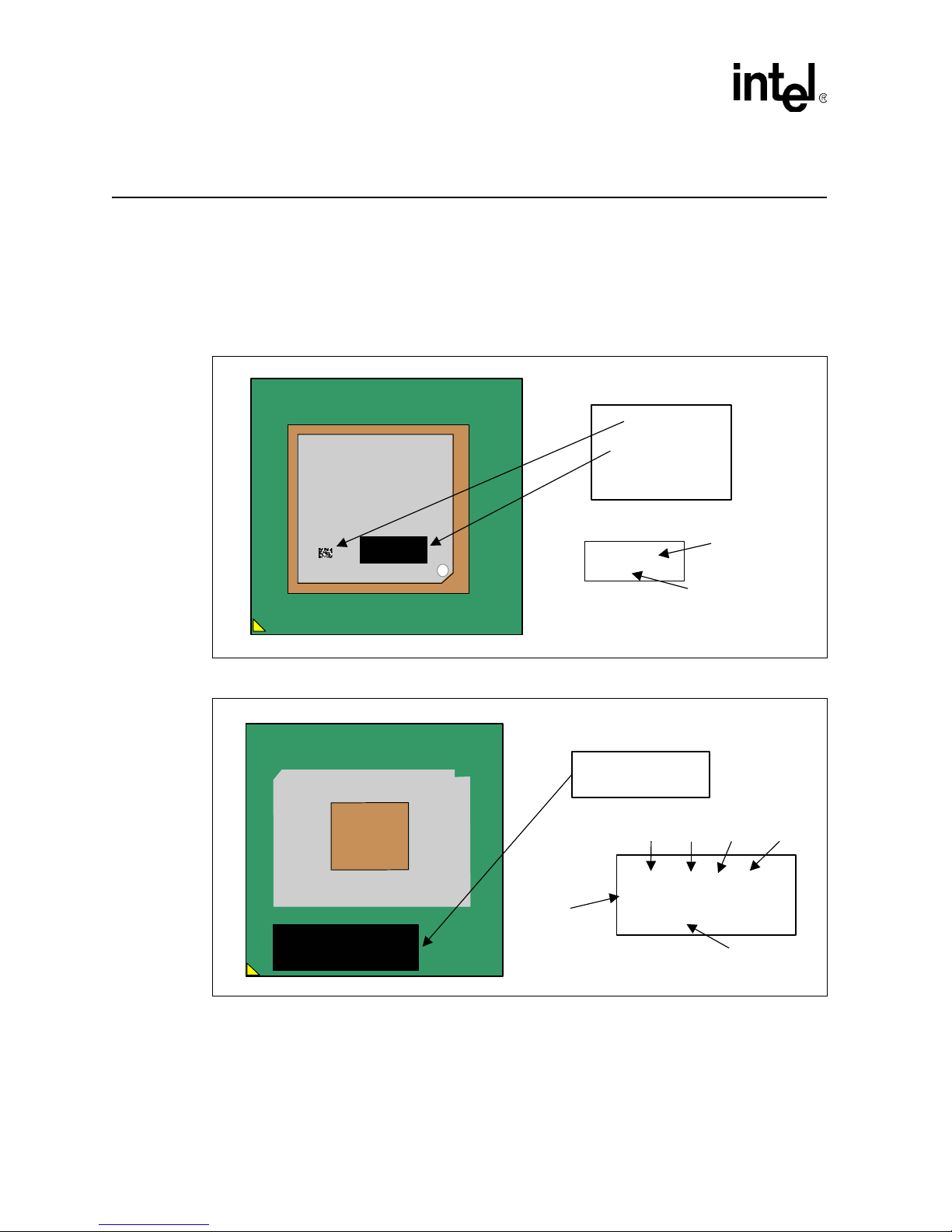
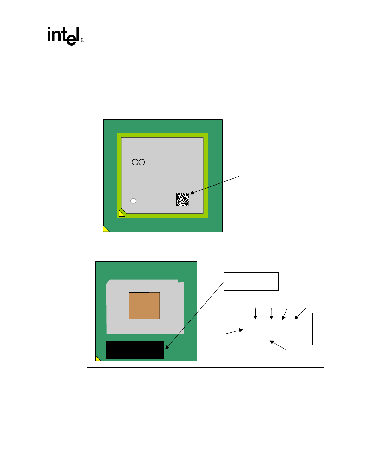
Identification Information
Identification Information
Intel® Xeon® Processor Markings, 256-KB Cache (603-pin
Interposer INT-mPGA Package)
Figure 1. Top Side Processor Marking
2D Matrix
OR
Intel® Xeon™
i(m) ©’01
Dynamic Laser
Mark Area
D0096109
0032
ATPO Mark
(8 Characters)
Serial Number
Mark
(4 digits)
Figure 2. Bottom Side Processor Marking
S-Spec
Country of
Assy
Dynamic Laser
Mark Area
Speed / Cache / Bus / Voltage
1700DP/256/400/1.7V
SL56N COSTA RICA
C0096109-0021
FPO – Serial #
(13 Characters)
10 Intel® Xeon® Processor Specification Update
Page 11
Identification Information
Intel® Xeon® Processor, 512-KB Cache, 400 and 533 MHz
FSB Markings, (603-pin Interposer INT-mPGA Package and
604-pin Fc-mPGA2 Package)
Figure 3. Top Side Processor Marking
Intel® Xeon™
i m c ‘02
2D Matrix Includes ATPO and
Serial Number (front end mark)
Figure 4. Bottom Side Processor Marking
S-Spec
Country of
Assy
Dynamic Laser
Mark Area
Speed / Cac he / Bus / Voltage
1800DP/512/400/1.5V
SL5Z8 COSTA RICA
C0096109-0021
FPO – Serial #
(13 Characters)
Intel® Xeon® Processor Specification Update 11
Page 12
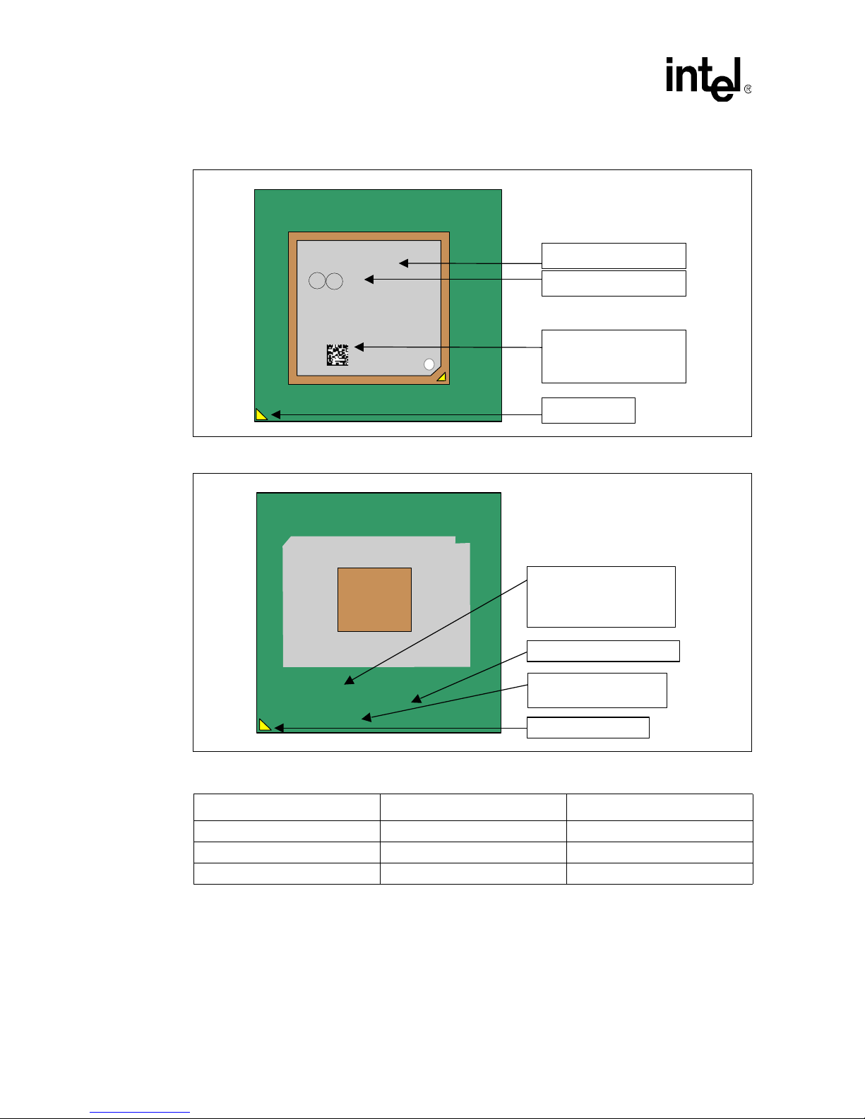
Identification Information
Figure 5. Example of Production Mark – Top View
Top View
Intel® Xeon™
i m c ‘01
Figure 6. Example of Production Mark – Bottom View
Brand
Copyright information
2D Matrix Includes
ATPO and Serial
Number (front end mark)
Pin A1 Triangle
Bottom View
Product Code with
feature infor m ation:
Speed/cache/bus/
voltage
S-Spec and Assembly Site
1700DP/256L2/400/1.7V
SL56N COSTA RICA
C0096109-0021
FPO and Serial Number
(End of Line M ark)
Pin A1 Triang le
The Intel Xeon processor can be identified by the following values:
1
Family
1111 0000 00001110
1111 0001 00001110
1111 0010 00001011
1. The Family corresponds to bits [11:8] of the EDX register after RESET, bits [11:8] of the EAX register after the Processor
Signature instruction is executed with a 1 in the EAX register, and the generation field of the Device ID register accessible
through Boundary Scan.
2. The Model corresponds to bits [7:4] of the EDX register after RESET, bits [7:4] of the EAX registe r after the Processor Signature
2 instruction is executed with a 1 in the EAX register, and the model field of the Device ID register accessible through Bound ary
Scan.
3. The Brand ID corresponds to bits [7:0] of the EBX register after the Processor Signat ure instruct ion is executed with a 1 in the
EAX register.
12 Intel® Xeon® Processor Specification Update
Model
2
Brand ID
3
Page 13

Identification Information
Cache and TLB descriptor parameters are provided in the EAX, EBX, ECX and EDX registers
after the Processor Signature instruction is executed with a 2 in the EAX register . Please refer to the
Intel Processor Identification and the Processor Signature Instruction Application Note (AP-485 )
for further information on the Processor Signature instruction.
Table 1. Intel
S-Spec
Number
SL4WX C1 0F0Ah 1.40/400 256-KB B0 603-pin micro-PGA
SL56G C1 0F0Ah 1.40/400 256-KB B0 603-pin micro-PGA
SL4WY C1 0F0Ah 1.50/400 256-KB B0 603-pin micro-PGA
SL4ZT C1 0F0Ah 1.50/400 256-KB B0 603-pin micro-PGA
SL56N C1 0F0Ah 1.70/400 256-KB B0 603-pin micro-PGA
SL56H C1 0F0Ah 1.70/400 256-KB B0 603-pin micro-PGA
SL5TD D0 0F12h 1.50/400 256-KB C0 603-pin micro-PGA
SL5U6 D0 0F12h 1.50/400 256-KB C0 603-pin micro-PGA
SL5TE D0 0F12h 1.70/400 256-KB C0 603-pin micro-PGA
SL5U7 D0 0F12h 1.70/400 256-KB C0 603-pin micro-PGA
SL5TH D0 0F12h 2/400 256-KB C0 603-pin micro-PGA
SL5U8 D0 0F12h 2/400 256-KB C0 603-pin micro-PGA
SL5Z8 B0 0F24h 1.80/400 512-KB 01 603-pin micro-PGA
SL622 B0 0F24h 1.80/400 512-KB 01 603-pin micro-PGA
SL5Z9 B0 0F24h 2/400 512-KB 01 603-pin micro-PGA
SL623 B0 0F24h 2/400 512-KB 01 603-pin micro-PGA
®
Xeon® Processor Identification and Package Information (Sheet 1 of 5)
Core
Stepping
Processor
Signature
Speed
Core/Front
Side Bus
(GHz/MHz)
L2 Size
(Kbytes)
L3 Size
(Kbytes)
Processor
Interposer
Revision
Package and
Revision
interposer with 31 mm
OLGA rev 2.0
interposer with 31 mm
OLGA rev 2.0
interposer with 31 mm
OLGA rev 2.0
interposer with 31 mm
OLGA rev 2.0
interposer with 31 mm
OLGA rev 2.0
interposer with 31 mm
OLGA rev 2.0
interposer with 31 mm
FC-BGA package
interposer with 31 mm
FC-BGA package
interposer with 31 mm
FC-BGA package.0
interposer with 31 mm
FC-BGA package
interposer with 31 mm
FC-BGA package 0
interposer with 31 mm
FC-BGA package
interposer with 35 mm
FC-BGA package
interposer with 35 mm
FC-BGA package
interposer with 35 mm
FC-BGA package
interposer with 35 mm
FC-BGA package
Notes
1, 4
1, 2, 4
1, 4
1, 2, 4
1, 4
1, 2, 4
1, 4
1, 2, 3,
4
1,4
1, 2, 3,
4
1, 3, 4
1, 2, 3,
4
1
1, 2
1
1, 2
Intel® Xeon® Processor Specification Update 13
Page 14

Identification Information
Table 1. Intel® Xeon® Processor Identification and Package Information (Sheet 2 of 5)
S-Spec
Number
SL5ZA B0 0F24h 2.20/400 512-KB 01 603-pin micro-PGA
SL624 B0 0F24h 2.20/400 512-KB 01 603-pin micro-PGA
SL687 B0 0F24h 2.40/400 512-KB 01 603-pin micro-PGA
SL65T B0 0F24h 2.40/400 512-KB 01 603-pin micro-PGA
SL6EL C1 0F27H 1.80/400 512-KB 01 603-pin micro-PGA
SL6JX C1 0F27H 1.80/400 512-KB 01 603-pin micro-PGA
SL6EM C1 0F27H 2/400 512-KB 01 603-pin micro-PGA
SL6JY C1 0F27H 2/400 512-KB 01 603-pin micro-PGA
SL6EN C1 0F27H 2.20/400 512-KB 01 603-pin micro-PGA
SL6JZ C1 0F27H 2.20/400 512-KB 01 603-pin micro-PGA
SL6EP C1 0F27H 2.40/400 512-KB 01 603-pin micro-PGA
SL6K2 C1 0F27H 2.40/400 512-KB 01 603-pin micro-PGA
SL6EQ C1 0F27H 2.60/400 512-KB 01 603-pin micro-PGA
SL6K3 C1 0F27H 2.60/400 512-KB 01 603-pin micro-PGA
SL6M7 C1 0F27H 2.80/400 512-KB 01 603-pin micro-PGA
SL6MS C1 0F27H 2.80/400 512-KB 01 603-pin micro-PGA
SL6NP C1 0F27H 2/533 512-KB 01 604-pin micro-PGA
SL6NQ C1 0F27H 2.40/533 512-KB 01 604-pin micro-PGA
Core
Stepping
Processor
Signature
Speed
Core/Front
Side Bus
(GHz/MHz)
L2 Size
(Kbytes)
L3 Size
(Kbytes)
Processor
Interposer
Revision
Package and
Revision
interposer with 35 mm
FC-BGA package
interposer with 35 mm
FC-BGA package
interposer with 35 mm
FC-BGA package
interposer with 35 mm
FC-BGA package
interposer with 35 mm
FC-BGA package
interposer with 35 mm
FC-BGA package
interposer with 35 mm
FC-BGA package
interposer with 35 mm
FC-BGA package
interposer with 35 mm
FC-BGA package
interposer with 35 mm
FC-BGA package
interposer with 35 mm
FC-BGA package
interposer with 35 mm
FC-BGA package
interposer with 35 mm
FC-BGA package
interposer with 35 mm
FC-BGA package
interposer with 35 mm
FC-BGA package
interposer with 35 mm
FC-BGA package
interposer with 42.5 mm
FC-PGA2 package
interposer with 42.5 mm
FC-PGA2 package
Notes
1
1, 2
1,2
2
2
2
2
2
2, 5
2, 5
14 Intel® Xeon® Processor Specification Update
Page 15

Identification Information
Table 1. Intel® Xeon® Processor Identification and Package Information (Sheet 3 of 5)
S-Spec
Number
SL6NR C1 0F27H 2.66/533 512-KB 01 604-pin micro-PGA
SL6NS C1 0F27H 2.8/533 512-KB 01 604-pin micro-PGA
SL6RQ C1 0F27H 2/533 512-KB 01 604-pin micro-PGA
SL6GD C1 0F27H 2.40/533 512-KB 01 604-pin micro-PGA
SL6GF C1 0F27H 2.66/533 512-KB 01 604-pin micro-PGA
SL6GG C1 0F27H 2.8/533 512-KB 01 604-pin micro-PGA
SL6GH
SL6RR
SL6GV C1 0F27H 1.60/400 512-KB 01 604-pin micro-PGA
SL6GV C1 0F27H 1.60/400 512-KB 01 604-pin micro-PGA
SL6W3
SL6YS
SL6W6
SL6YT
SL6W7
SL6YU
SL6W8
SL6YV
SL6W9
SL6YW
SL6WA
SL6YX
SL6WB
SL6YY
SL6XK D1 0F29H 1.60/400 512-KB 01 604-pin micro-PGA
SL6XL D1 0F29H 2/400 512-KB 01 604-pin micro-PGA
Core
Stepping
C1 0F27H 3.06/533 512-KB 01 604-pin micro-PGA
D1 0F29H 1.80/400 512-KB 01 603-pin micro-PGA
D1 0F29H 2/400 512-KB 01 603-pin micro-PGA
D1 0F29H 2.20/400 512-KB 01 603-pin micro-PGA
D1 0F29H 2.40/400
D1 0F29H 2.60/400
D1 0F29H 2.8/0400
D1 0F29H 3/400
Processor
Signature
Speed
Core/Front
Side Bus
(GHz/MHz)
L2 Size
(Kbytes)
512-KB
512-KB
512-KB
512-KB
L3 Size
(Kbytes)
Processor
Interposer
Revision
01 603-pin micro-PGA
01 603-pin micro-PGA
01 603-pin micro-PGA
01 603-pin micro-PGA
Package and
Revision
interposer with 42.5 mm
FC-PGA2 package
interposer with 42.5 mm
FC-PGA2 package
interposer with 42.5 mm
FC-PGA2 package
interposer with 42.5 mm
FC-PGA2 package
interposer with 42.5 mm
FC-PGA2 package
interposer with 42.5 mm
FC-PGA2 package
interposer with 42.5 mm
FC-PGA2 package
interposer with 42.5 mm
FC-PGA2 package
interposer with 42.5 mm
FC-PGA2 package
interposer with 35 mm
FC-BGA package
interposer with 35 mm
FC-BGA package
interposer with 35 mm
FC-BGA package
interposer with 35 mm
FC-BGA package
interposer with 35 mm
FC-BGA package
interposer with 35 mm
FC-BGA package
interposer with 35 mm
FC-BGA package
interposer with 42.5 mm
FC-PGA2 package
interposer with 42.5 mm
FC-PGA2 package
Notes
2, 5
2, 5
5
5
5
5
5, 6
2, 6
7
7
3
2
3
2
3
2
3
2
3
2
3
2
3, 6
2
7
7
Intel® Xeon® Processor Specification Update 15
Page 16

Identification Information
Table 1. Intel® Xeon® Processor Identification and Package Information (Sheet 4 of 5)
S-Spec
Number
SL74T D1 0F29H 2.40/533 512-KB 01 604-pin micro-PGA
SL6VK
SL6YM
SL6VL
SL6YN
SL6VM
SL6NR
SL6VN
SL6YQ
SL6VP
SL6YR
SL73K
SL72C
SL73L
SL72D
SL73M
SL72E
SL73N
SL72F
SL73P
SL72G
SL73Q
SL72Y
SL7AE
SL7BW
SL7D5
SL7DG
SL7D4
SL7DF
SL8TJ L0 0F29h 0F29H 2.40/533 512-KB 01 604-pin micro-PGA
SL8TK L0 0F29H 2.80/533 512-KB 01 604-pin micro-PGA
Core
Stepping
D1 0F 29H 2/533 512-KB 01 604-pin micro-PGA
D1 0F 29H 2.40/533 512-KB 01 604-pin micro-PGA
D1 0F 29H 2.66/533 512-KB 01 604-pin micro-PGA
D1 0F29H 2.80/533
D1 0F29H 3.06/533
M0 0F25H 2/533
M0 0F25H 2.40/533
M0 0F25H 2.66/533
M0 0F25H 2.80/533
M0 0F25H 3.06/533
M0 0F25H 3.2/533
M0 0F25H 3.2/533
M0 0F25H 2.80/533
M0 0F25H 2.40/533
Processor
Signature
Speed
Core/Front
Side Bus
(GHz/MHz)
L2 Size
(Kbytes)
512-KB
512-KB
512-KB
512-KB
512-KB
512-KB
512-KB 1-MB
512-KB 1-MB
512-KB 2-MB
512-KB 1-MB
512-KB 1-MB
L3 Size
(Kbytes)
Processor
Interposer
Revision
01 604-pin micro-PGA
01 604-pin micro-PGA
01 604-pin micro-PGA
01 604-pin micro-PGA
01 604-pin micro-PGA
01 604-pin micro-PGA
01 604-pin micro-PGA
01 604-pin micro-PGA
01 604-pin micro-PGA
01 604-pin micro-PGA 6
01 604-pin micro-PGA 6
Package and
Revision
interposer with 42.5 mm
FC-PGA2 package
Interposer with 42.5 mm
FC-PGA2 package
interposer with 42.5 mm
FC-PGA2 package
interposer with 42.5 mm
FC-PGA2 package
interposer with 42.5 mm
FC-PGA2 package
interposer with 42.5 mm
FC-PGA2 package
interposer with 42.5 mm
FC-PGA2 package
interposer with 42.5 mm
FC-PGA2 package
interposer with 42.5 mm
FC-PGA2 package
interposer with 42.5 mm
FC-PGA2 package
interposer with 42.5 mm
FC-PGA2 package
interposer with 42.5 mm
FC-PGA2 package
interposer with 42.5 mm
FC-PGA2 package
interposer with 42.5 mm
FC-PGA2 package
interposer with 42.5 mm
FC-PGA2 package
Notes
7
5
2
5
2
5
2
5
2
5, 6
2
2
2
2
2
2, 6, 8
6, 8
2, 6, 8
6, 8
2, 6, 9
6
2, 6,8
2, 6, 8
7
5
2
16 Intel® Xeon® Processor Specification Update
Page 17

Identification Information
Table 1. Intel® Xeon® Processor Identification and Package Information (Sheet 5 of 5)
S-Spec
Number
Core
Stepping
Processor
Signature
Core/Front
Side Bus
L2 Size
(Kbytes)
L3 Size
(Kbytes)
(GHz/MHz)
SL8TL L0 0F29H 2.40/533 512-KB 01 604-pin micro-PGA
SL8SE L0 0F29H 2/400 512-KB 01 604-pin micro-PGA
SL8TH L0 0F29H 1.60/400 512-KB 01 604-pin micro-PGA
Speed
Processor
Interposer
Revision
Package and
Revision
interposer with 42.5 mm
FC-PGA2 package
interposer with 42.5 mm
FC-PGA2 package
interposer with 42.5 mm
FC-PGA2 package
Notes
5
2
7
7
NOTES:
1. The Intel
®
Xeon® processor listed here is installed onto a micro pin grid array (mPGA) interposer. The overall processor
package is called INT-mPGA.
2. These parts are Intel boxed processors.
3. FC-BGA packaging maintains form, fit, and functionality when compared to OLGA packaging. Users may notice a color change.
4. These parts require the inputs from A20M#, IGNNE#, LINT[1]/NMI and LINT[0]/INTR pins during RESET to set the correct core
to bus frequency ratio.
5. These parts are the Intel
6. These parts have a VID of 1.525V.
7. These parts are the Low Voltage Intel
8. These parts are the Intel
9. These parts are the Intel
®
Xeon® Processor with 533 MHz Front Side Bus.
®
®
Xeon® Processor with 1-MB L3 Cache.
®
Xeon® Processor with 2-MB L3 Cache.
Xeon® Processor.
Intel® Xeon® Processor Specification Update 17
Page 18

Mixed Steppings in DP Systems
Mixed Steppings in DP Systems
Intel Corporation fully supports mixed steppings of Intel Xeon processors. The following list and
processor matrix describes the requirements to support mixed steppings:
• Mixed steppings are only supported with processors that have identical family numbers as
indicated by the Processor Signature instruction. The Intel Xeon processor is available with
two different Model numbers as indicated by the Processor Signature. Please refer to Table 2
for details regarding inclusion of processors with mixed Processor Signature/Core steppings.
• While Intel has done nothing to specifically prevent processors operating at differing
frequencies from functioning within a multiprocessor system, there may be uncharacterized
errata that exist in such configurations. Intel does not support such configurations. In mixed
stepping systems, all processors must operate at identical frequencies (i.e., the highest
frequency rating commonly supported by all processors).
• While there are no known issues associated with the mixing of processors with differing cache
sizes in a multiprocessor system, and Intel has done nothing to specifically prevent such
system configurations from operating, Intel does not support such configurations since there
may be uncharacterized errata that exist. In mixed stepping systems, all processors must be of
the same cache size.
• While Intel believes that certain customers may wish to perform validation of system
configurations with mixed frequency or cache sizes, and that those efforts are an acceptable
option to our customers, customers would be fully responsible for the validation of such
configurations.
• Intel requires that the proper microcode update be loaded on each processor operating in a
multiprocessor system. Any processor that does not have the proper microcode update loaded
is considered by Intel to be operating out of specification.
• The workarounds identified in this and following specification updates must be properly
applied to each processor in the system. Certain errata are specific to the multiprocessor
environment and are identified in Table 2 found at the end of this section. Errata for all
processor steppings will affect system performance if not properly worked around. Also see
Table 1 for additional details on which processors are affected by specific errata.
• In mixed stepping systems, the processor with the lowest feature-set, as determined by the
Processor Signature Feature Bytes, must be the bootstrap processor (BSP). In the event of a tie
in feature-set, the tie should be resolved by selecting the BSP as the processor with the lowest
stepping as determined by the Processor Signature instruction.
In the following processor matrix, “NI” indicates that there are currently no known issues
associated with mixing these steppings. A number indicates that a known issue has been identified
as listed in the table following the matrix. “X” indicates the processors cannot be mixed. A dual
processor system using mixed processor steppings must assure that errata are addressed
appropriately for each processor.
18 Intel® Xeon® Processor Specification Update
Page 19

Mixed Steppings in DP Systems
Table 2. DP Platform Matrix for the Intel® Xeon® Processor
Processor
Signature/Core
Stepping
0F0Ah/C1 NI Note 1 X X X X X
0F12h/D0 Note 1 NI X X X X X
0F24h/B0 X X NI NI NI NI X
0F27h/C1 X X NI NI NI NI X
0F29h/D1 X X NI NI NI NI X
0F25h/M0 X X NI NI NI NI NI
0F29h/L0 X X NI NI NI NI X
NOTES:
1. Some of these processors are affected by errata, which may affect the features an MP system is able to support. See the
Table 1 for details on which processors are affected by these errata.
2. This Matrix also applies to the Intel
®
Intel
Xeon® Processor with 1-MB L3 cache, and Intel® Xeon® Processor with 2-MB L3 cache.
3. This only applies to 0F25h stepping without L3 cache.
4. This only applies to 0F25h stepping with L3 cache.
0F0Ah/C1 0F12h/D0 0F24h/B0 0F27h/C1 0F29h/D1 0F25h/M0
®
Xeon® Processor with 533 MHz Front Side Bus, Low Voltage Intel® Xeon® Processor,
2
3
0F25h/M0
4
Intel® Xeon® Processor Specification Update 19
Page 20

Summary Table of Changes
Summary Table of Changes
The following table indicates the Specification Changes, Errata, Specification Clarifications or
Documentation Changes, which apply to the listed MCH steppings. Intel intends to fix some of the
errata in a future stepping of the component, and to account for the other outstanding issues
through documentation or Specification Changes as noted. This table uses the following notations:
Codes Used in Summary Table
X: Erratum, Specification Change or Clarification that applies to the
given processor stepping.
(No mark) or (Blank Box): This erratum is fixed in listed stepping or specification change does
not apply to listed stepping.
Doc: Document change or update that will be implemented.
Plan Fix: This erratum may be fixed in a future of the product.
Fixed: This erratum has been previously fixed.
No Fix: There are no plans to fix this erratum.
PKG: This column refers to errata on the Intel Xeon processor substrate.
AP APIC-related erratum.
Change bar to left of table row indicates this item is either new or
modified from the previous version of this document.
Each Specification Update item is prefixed with a capital letter to distinguish the product. The key
below details the letters that are used in Intel’ s microprocessor Specification Updates:
A=Intel
B = Mobile Intel
C=Intel
D = Dual-Core Intel
E=Intel
F=Intel
G=Intel
H = Mobile Intel
J = 64-bit Intel
K = Mobile Intel
L=Intel
M = Mobile Intel
N=Intel
O=Intel
P=Intel
Q = Mobile Intel
®
Pentium® II processor
®
®
Celeron® processor
®
Pentium® III processor
®
Pentium® processor Extreme Edition and Intel® Pentium® D processor
®
Pentium® III Xeon™ processor
®
Celeron® D processor
®
®
Xeon® processor MP
®
Xeon® processor
Pentium® II processor
®
Xeon® Processor 2.8 GHz
®
Celeron® processor at 466/433/400/366/333/300 and 266 MHz
®
Xeon® processor MP with 1MB L2 cache
®
Pentium® III processor
®
Celeron® processor
Pentium® 4 processor
®
Pentium® 4 processor supporting Hyper-Threading Technology on 90-nm
process technology
R=Intel
S = 64-bit Intel
®
Pentium® 4 processor on 90 nm process
®
Xeon® processor with 800 MHz system bus (1 MB and 2 MB L2 cache
versions)
20 Intel® Xeon® Processor Specification Update
Page 21

Summary Table of Changes
T = Mobile Intel® Pentium® 4 processor-M
U = 64-bit Intel
V = Mobile Intel
W= Intel
X=Intel
Y=Intel
Z = Mobile Intel
AA = Intel
®
Xeon® processor MP with up to 8MB L3 Cache
®
®
Celeron® M processor
®
Pentium® M processor on 90nm process with 2-MB L2 Cache
®
Pentium® M processor
®
Pentium® processor Extreme Edition and Intel® Pentium® D processor on 65 nm
Celeron® processor on .13 Micron Process in Micro-FCPGA Package
®
Pentium® 4 processor with 533 MHz system bus
process
AB = Intel
AC = Intel
AG= Dual-Core Intel
AH= Intel
AI= Intel
®
Pentium® 4 processor on 65 nm process
®
Celeron® Processor in 478 Pin Package
®
Core™2 Duo mobile Processor
®
Core™2 Extreme Processor X6800 and Intel® Core™2 Duo Desktop Processor
®
Xeon® Processor 5100 Series
E6000 Sequence
AJ = Quad-Core Intel® Xeon® Processor 5300 Series
AL= Dual-Core Intel
AP= Dual-Core Intel
®
Xeon® Processor 7100 Series
® Xeon® Processor 3000 Series
Note: The Specification Updates for the Pentium
products do not use this convention.
®
processor, Pentium® Pro processor, and other Intel
Intel® Xeon® Processor Specification Update 21
Page 22

Summary Table of Changes
Errata (Sheet 1 of 4)
No.
P1 XX FixedUC Code in same line as write back (WB) data may
P2 XXXXXXXNo FixTransaction is not retried after BINIT#
P3 XXXXXXXNo FixInvalid opcode 0FFFh requires a ModRM byte
P4 XXXXXXXNo FixWhen in no-fill mode (CR0.CD=1) the memory type
P5 XXXXXXXNo FixProcessor may hang due to speculative page
P6 XX FixedWriting a performance counter may result in an
P7 XX FixedPerformance counter may contain incorrect value
P8 XFixedREP MOV instruction with overlapping source and
P9 XXXXXXXNo FixMemory type of the load lock different from its
P10 XXXXXXXNo FixMachine check architecture error reporting and
P11 XXXXXXXNo FixDebug mechanisms may not function as expected
P12 XFixedProcessor may live-lock if PDEs or PTEs are in UC
P13 XFixedThermal status log bit may not be set when the
P14 XX FixedProcessor may timeout waiting for a device to
P15 XXXXXXXNo FixCascading of performance counters does not work
P16 XXXXXXXNo FixEMON event counting of x87 loads may not work
P17 XX FixedSimultaneous code breakpoint and uncorrectable
P18 XX FixedSoftware controlled clock modulation using a
P19 XFixedRFO with ECC error may result in incorrect data
P20 XFixedSpeculative page-fault may cause livelock
P21 XFixedPAT index MSB may be calculated incorrectly
P22 XXXXXXXNo FixSystem bus interrupt messages without data and
P23 XX Fixed
P24 XXX FixedBus invalidate line requests that returns
P25 XFixedMultiprocessor boot protocol may not complete
C1/
0F0Ah
D0/
0F12h
B0/
0F24h
C1/
0F27h
D1/
0F29h
M0/
0F25h
L0/
0F29h
Plans Errata
lead to data corruption
of large (PSE-4M and PAE-2M) pages are wrongly
forced to uncacheable
walks to nonexistent system memory
incorrect counter value
after being stopped
destination may result in data corruption
corresponding store unlock
recovery may not work as expected
space
thermal control circuit is active
respond after 0.67 seconds
correctly when forced overflow is enabled
as expected
error results in processor hang
12.5% or 25% duty cycle may cause the processor
to hang
which receive a Hard failure response may hang
the processor
SQRTPD and SQRTSD may return QNaN
indefinite instead of negative zero
unexpected data may result in L1 cache corruption
with an IOQ depth of one
22 Intel® Xeon® Processor Specification Update
Page 23

Errata (Sheet 2 of 4)
Summary Table of Changes
No.
P26 XXXXXXXNo FixThe processor signals page-fault exception (#pf)
P27 XXX FixedIncorrect data may be returned when page tables
P28 XXXXXXXNo FixFSW may not be completely restored after
P29 XXX FixedWrite combining (WC) load may result in an
P30 XXXXXXXNo FixProcessor provides a 4-byte store unlock after an
P31 XXX FixedMultiple accesses to the same S-state L2 cache
P32 XXXXXXXNo FixIA32_MC0_ADDR and IA32_MC0_MISC registers
P33 XXXXXXXNo FixWhen the processor is in the system management
P34 XXXXXXXNo FixAssociated counting logic must be configured
P35 XXX FixedLivelock may occur when bus parking is disabled
P36 XXX FixedCR2 May be incorrect or an incorrect page-fault
P37 XX FixedBuffer on resistance may exceed specification
P38 XFixedInstruction pointer stored on stack may become
P39 XXXXXNo FixShutdown and IERR# may result due to a machine
P40 XFixedHyper-Threading Technology enabled processors
P41 XFixedGlobal bit incorrectly set for secondary logical
P42 XFixedMachine check exception (MCE) observed on DP
P43 XXXXXPlan FixBPM[5:3]# VIL does not meet specification
P44 XXXXXNo FixProcessor may hang under certain frequencies and
P45 XXXXXXXNo FixSystem may hang if a fatal cache error causes bus
P46 XXX FixedL2 cache may contain stale data in the exclusive
C1/
0F0Ah
D0/
0F12h
B0/
0F24h
C1/
0F27h
D1/
0F29h
M0/
0F25h
L0/
0F29h
Plans Errata
instead of alignment check exception (#ac) on an
unlocked cmpxchg8b instruction
are located in write combining (WC) memory
page-fault on FRSTOR or FLDENV instructions
unintended address on system bus
8-byte load lock
line and ECC error combination may result in loss
of cache coherency
will contain invalid or stale data following a data,
address, or response parity error
mode (SMM), debug registers may be fully
writeable
when using event selection control (ESCR) MSR
error code may be pushed on to stack after
execution of an LSS instruction
invalid
check exception on a Hyper-threading Technology
enabled processor
may hang in the presence of extensive
self-modifying code
processors in ITLB
platforms
12.5% STPCLK# duty cycle
write line (BWL) transaction to occur to the same
cache line address as an outstanding bus read line
(BRL) or bus read-invalidate line (BRIL)
state
Intel® Xeon® Processor Specification Update 23
Page 24

Summary Table of Changes
Errata (Sheet 3 of 4)
No.
P47 XXXXXXXNo FixRe-mapping the APIC base address to a value less
P48 XXXXXNo FixErroneous BIST result found in EAX register after
P49 XXX FixedProcessor does not flag #GP on non-zero write to
P50 XXXXX XNo FixSimultaneous assertion of A20M# and INIT# may
P51 XX FixedProcessor does not respond to break requests
P52 XXX FixedGlitches on address and data strobe signals may
P53 XXXXXXXNo FixA write to an APIC Register Sometimes May
P54 XXXPlan FixSTPCLK# signal assertion under certain conditions
P55 XXXXPlan FixStore to load data forwarding may result in
P56 XXXXPlan FixITP cannot continue single step execution after the
P57 XXXXXXXNo FixParity error in the L1 cache may cause the
P58 XXXXXXXPlan FixThe TCK input in the test access port (TAP) is
P59 XXXXXXXNo FixDisabling a local APIC disables both logical
P60 XXXXXXXNo FixUsing STPCLK and executing code from very slow
P61 X Plan Fix Simultaneous cache line eviction from L2 and L3
P62 XXXXXXXNo FixThe state of the resume flag (RF flag) in a
P63 XXXXNo FixChanges to CR3 register do not fence pending
P64 XXXXXPlan FixSimultaneous page-faults at similar page offsets on
P65 XXXXXXXNo FixA 16-bit address wrap resulting from a near branch
P66 XXXXXXXNo FixLocks and SMC detection may cause the
P67 XXXXXXXNo FixIncorrect debug exception (#DB) may occur when
C1/
0F0Ah
D0/
0F12h
B0/
0F24h
C1/
0F27h
D1/
0F29h
M0/
0F25h
L0/
0F29h
Plans Errata
than or equal to 0xDC001000 may cause I/O and
special cycle failure
reset
certain MSRs
result in incorrect data fetch
from ITP
cause system shutdown
Appear to Have Not Occured
may cause a system hang
switched data bytes
first breakpoint
processor to hang
sensitive to low clock edge rates and prone to
noise coupling onto TCK's rising or falling edges
processor on a Hyper-Threading Technology
enabled processor
memory could lead to a system hang
caches may result in the write back of stale data
task-state segment (TSS) may be incorrect
instruction page
both logical processors of an Hyper-Threading
Technology enabled processor may cause
application failure
(jump or call) may cause an incorrect address to be
reported to the #GP exception handler
processor to temporarily hang
a data breakpoint is set on a FP instruction
24 Intel® Xeon® Processor Specification Update
Page 25

Errata (Sheet 4 of 4)
Summary Table of Changes
No.
P68 XNo FixModified cache line eviction from L2 cache may
P69 XXXXXXXNo FixxAPIC may not report some illegal vector errors
P70 XXXXXXXNo FixIncorrect duty cycle is chosen when On-Demand
P71 XXXXXXXPlan FixMemory aliasing of pages as uncacheable memory
P72 XXXPlan FixA timing marginality in the Instruction Decoder unit
P73 XXXXXXXNo FixMissing Stop Grant Acknowledge special bus cycle
P74 XXXXXXXNo FixMachine check exceptions may not update
P75 XXXXXXXNo FixStores to page tables may not be visible to page
P76 XXXPlan FixA timing marginality in the Arithmetic Logic Unit
P77 XXXXXXXNo FixWith Trap Flag (TF) asserted, FP instruction that
P78 XXXXXXXNo FixPDE/PTE loads and continuous locked updates to
P79 XXXXXXXNo FixBranch Trace Store (BTS) and Precise Event
P80 XXXXXXXNo FixMemory Ordering Failure may occur with Snoop
P81 XXXXXXXNo FixControl Register 2 (CR2) can be updated during a
P82 XXXXXXXNo FixWriting the Local Vector Table (LVT)
P83 XXXXXXXNo FixThe Processor May Report a #TS Instead of a #GP
C1/
0F0Ah
D0/
0F12h
B0/
0F24h
C1/
0F27h
D1/
0F29h
M0/
0F25h
L0/
0F29h
Plans Errata
result in write back of stale data
Clock Modulation is enabled in a processor
supporting Hyper-Threading Technology
type and write back (WB) may hang the system
may cause an unpredictable application behavior
and/or system hang
may cause a system hang
Last-Exception Record MSRs (LERs)
walks for subsequent loads without serializing or
invalidating the page table entry
(ALU) may cause indeterminate behavior
triggers an unmasked FP exception may take
single step trap before retirement of instruction
the same cache line may cause a system livelock
Based Sampling (PEBS) may update memory
outside the BTS/PREBS buffer
Filtering Third-Party Agents after Issuing and
completing a BWIL (Bus Write Invalidate Line) or
BLW (Bus Locked Write) transaction
REP MOVS/STOS instruction with Fast Strings
enabled
when an Interrup t is Pending May Cause an
Unexpected Interrupt
Fault
Intel® Xeon® Processor Specification Update 25
Page 26

Summary Table of Changes
Specification Changes
No. SPECIFICATION CHANGES
P1 Context ID feature added to processor signature instruction feature Flags/IA32_MISC_Enable registers
Specification Clarifications
No. SPECIFICATION CLARIFICATIONS
P1 Maximum ITCC specification correction
P2 Specification Clarification with respect to Time-Stamp Counter
Documentation Changes
No. DOCUMENTATION CHANGES
None for this revision of the Specification Update.
26 Intel® Xeon® Processor Specification Update
Page 27

Errata
Errata
P1 UC Code in same line as write back (WB) data may lead to data corruption
Problem: This erratum occurs when both code (being accessed as uncacheable [UC] or write combining
[WC]) and data (being accessed as write back [WB]) are placed in the same cache line. The UC
fetch will cause the processor to self-snoop and generate an implicit WB. The data supplied by this
implicit WB may be corrupted due to the way the processor is currently handling self-modifying
code.
Implication: UC code located in the same cache line as WB data may lead to data corruption.
Workaround: UC or WC code should not be located in the same 64-byte cache line as any location that is being
stored to with WB data.
Status: For the steppings effected, see the Summary Table of Changes.
P2 Transaction is not retried after BINIT#
Problem: If the first transaction of a locked sequence receives a HITM# and DEFER# during the snoop phase
it should be retried and the locked sequence restarted. However, if BINIT# is also asserted during
this transaction, the transaction will not be retried.
Implication: When this erratum occurs, locked transactions will not be retried.
Workaround: None at this time.
Status: For the steppings effected, see the Summary Table of Changes.
P3 Invalid opcode 0FFFh requires a ModRM byte
Problem: Some invalid opcodes require a ModRM byte and other following bytes, while others do not. The
invalid opcode 0FFFh did not require a ModRM in previous generation microprocessors such as
Pentium II or Pentium III processors, but it is required in the Intel Xeon processor
Implication: The use of an invalid opcode 0FFFh without the ModRM byte may result in a page or limit fault on
the Intel Xeon processor.
Workaround: To avoid this erratum use ModRM byte with invalid 0FFFh opcode.
Status: For the steppings affected, see the Summary Table of Changes.
P4 When in no-fill mode (CR0.CD=1) the memory type of large (PSE-4M and
PAE-2M) pages are wrongly forced to uncacheable
Problem: When the processor is operating in no-fill mode (CR0.CD=1), the page miss hardware incorrectly
forces the memory type of large (PSE-4M and PAE-2M) pages to UC memory type regardless of
the MTRR settings. By forcing the memory type of these pages to UC, load operations, which
should hit valid data in the L1 cache, are forced to load the data from system memory. Some
applications will lose the performance advantage associated with the caching permitted by other
memory types.
Implication: This erratum may result in some performance degradation when using no-fill mode with large
pages.
Workaround: None at this time.
Status: For the steppings affected, see the Summary Table of Changes
Intel® Xeon® Processor Specification Update 27
Page 28

Errata
P5 Processor may hang due to speculative page walks to nonexistent system
memory
Problem: A load operation issued speculatively by the processor that misses the data translation lookaside
buffer (DTLB) results in a page walk. A branch instruction older than the load retires so that this
load operation is now in the mispredicted branch path. Due to an internal boundary condition, in
some instances the load is not canceled before the page walk is issued.
The page miss handler (PMH) starts a speculative page walk for the load and issues a cacheable
load of the page directory entry (PDE). This PDE load returns data that points to a page table entry
in uncacheable (UC) memory. The PMH issues the PTE Load to UC space, which is issued on the
front side bus. No response comes back for this load PTE operation since the address is pointing to
system memory, which does not exist.
This load to non-existent system memory causes the processor to hang because other bus requests
are queued up behind this UC PTE load, which never gets a response. If the load was accessing
valid system memory, the speculative page-walk would successfully complete and the processor
would continue to make forward progress.
Implication: Processor may hang due to speculative page walks to non-exi stent system memory.
Workaround: Page directories and page tables in UC memory space must point to system memory that exists.
Status: For the steppings affected, see the Summary Table of Changes.
P6 Writing a performance counter may result in an incorrect counter value
Problem: Accessing a performance counter also enables the counter input so that writing one half of the
counter can cause the other half to increment. When a performance counter is written and the event
counter for the event being monitored is non-zero, the performance counter will be incremented by
the value on that event counter. Because the upper eight bits of the performance counter are not
written at the same time as the lower 32 bits, the increment due to the non-zero event counter may
cause a carry to the upper bits such that the performance counter contains a value higher than what
was written. The worst-case error caused by this can be about 4 billion counts.
Implication: When this erratum occurs, the performance counter will contain a different value from that which
was written.
Workaround: If the performance counter is set to select a null event and the counter configuration control register
(CCCR) for that counter has its compare bit set to zero, before the performance counter is written,
this erratum will not occur.
Status: For the steppings affected, see the Summary Table of Changes.
P7 Performance counter may contain incorrect value after being stopped
Problem: If a performance counter is stopped on the precise internal clock cycle where the intermediate carry
from the lower 32 bits of the counter to the upper eight bits occurs, the intermediate carry is lost.
Implication: When this erratum occurs the performance coun ter m ay contain a value about 4 billion (
than it should.
Workaround: Since this erratum does not occur if the performance counters are read when running, a possible
workaround is to read the counter before stopping it.
32) less
2
Status: For the steppings affected, see the Summary Table of Changes.
P8 REP MOV instruction with overlapping source and destination may result in
data corruption
Problem: When fast strings are enabled and a REP MOV instruction is used to move a string and the source
and destination strings overlap by 56 bytes or less, data corruption may occur.
28 Intel® Xeon® Processor Specification Update
Page 29

Errata
Implication: When this erratum occurs, data corruption may occur.
Workaround: It is possible for the BIOS to contain a workaround for this erratum.
Status: For the steppings affected, see the Summary Table of Changes.
P9 Memory type of the load lock different from its corresponding store unlock
Problem: A use-once protocol is employed to ensure that the processor in a multi-agent system may access
data that is loaded into its cache on a RFO operation at least once before it is snooped out by
another agent. This protocol is necessary to avoid a multi-agent livelock scenario in which the
processor cannot gain ownership of a line and modify it before that data is snooped out by another
agent. In the case of this erratum, split load lock instructions incorrectly trigger the use-once
protocol. A load lock operation accesses data that splits across a page boundary with both pages of
WB memory type. The use-once protocol activates and the memory type for the split halves get
forced to UC. Since use-once does not apply to stores, the store unlock instructions go out as WB
memory type. The full sequence on the bus is: locked partial read (UC), partial read (UC), partial
write (WB), locked partial write (WB). The use-once protocol should not be applied to load locks.
Implication: When this erratum occurs, the memory type of the load lock will be different than the memory type
of the store unlock operation. This behavior (load locks and store unlocks having different memory
types) does not introduce any functional failures such as system hangs or memory corruption.
Workaround: None at this time.
Status: For the steppings affected, see the Summary Table of Changes.
P10 Machine check architecture error reporting and recovery may not work as
expected
Problem: When the processor detects errors it should attempt to report and/or recover from the error. In the
situations described below, the processor does not report and/or recover from the error(s) as
intended.
• When a transaction is deferred during the snoop phase and subsequently receives a Hard
Failure response, the transaction should be removed from the bus queue so that the processor
may proceed. Instead, the transaction is not properly removed from the bus queue, the bus
queue is blocked, and the processor will hang.
• When a hardware prefetch results in an uncorrectable tag error in the L2 cache,
MC0_STATUS.UNCOR and MC0_STATUS.PCC are set but no machine check exception
(MCE) is signaled. No data loss or corruption occurs because the data being prefetched has not
been used. If the data location with the uncorrectable tag error is subsequently accessed, an
MCE will occur. However , upon this MCE, or any other subsequent MCE,.the information for
that error will not be logged because MC0_STATUS.UNCOR has already been set and the
MCA status registers will not contain information about the error which caused the MCE
assertion but instead will contain information about the prefetch error event.
• When the reporting of errors is disabled for machine check architecture (MCA) Bank 2 by
setting all MC2_CTL register bits to 0, uncorrectable errors should be logged in the
IA32_MC2_STATUS register but no m achine-check exception should be generated.
Uncorrectable loads on bank 2, which would normally be logged in the IA32_MC2_STATUS
register, are not logged.
• When one half of a 64 byte instruction fetch from the L2 cache has an uncorrectable error and
the other 32 byte half of the same fetch from the L2 cache has a correctable error , the processor
will attempt to correct the correctable error but cannot proceed due to the uncorrectable error.
When this occurs the processor will hang.
• When an L1 cache parity error occurs, the cache controller logic should write the physical
address of the data memory location that produced that error into the IA32_MC1_ADDR
REGISTER (MC1_ADDR). In some instances of a parity error on a load operation that hits
Intel® Xeon® Processor Specification Update 29
Page 30

Errata
the L1 cache, the cache controller logic may write the physical address from a subsequent load
or store operation into the IA32_MC1_ADDR register.
• When an error exists in the tag field of a cache line such that a read for ownership (RFO)
issued by the processor hits multiple tag fields in the L2 cache (the correct tag and the tag with
the error) and the accessed data also has a correctable error, the processor will correctly log the
multiple tag match error but will hang when attempting to execute the machine check
exception handler.
• If a memory access receives a machine check error on both 64 byte halves of a 128-byte L2
cache sector, the IA32_MC0_STATUS register records this event as multiple errors, i.e., the
valid error bit and the overflow error bit are both set indicating that a machine check error
occurred while the results of a previous error were in the error-reporting bank. The
IA32_MC1_STATUS register should also record this event as multiple errors but instead
records this event as only one correctable error.
• The overflow bit should be set to indicate when more than one error has occurred. The
overflow bit being set indicates that more than one error has occurred. Because of this erratum,
if any further errors occur, the MCA overflow bit will not be updated, thereby incorrectly
indicating only one error has been received.
• If an I/O instruction (IN, INS, REP INS, OUT, OUTS, or REP OUTS) is being executed, and if
the data for this instruction becomes corrupted, the processor will signal a MCE. If the
instruction is directed at a device that is powered down, the processor may also receive an
assertion of SMI#. Since MCEs have higher priority, the processor will call the MCE handler,
and the SMI# assertion will remain pending. However, while attempting to execute the first
instruction of the MCE handler, the SMI# will be recognized and the processor will attempt to
execute the SMM handler. If the SMM handler is successfully completed, it will attempt to
restart the I/O instruction, but will not have the correct machine state due to the call to the
MCE handler. This can lead to failure of the restart and shutdown of the processor.
• If PWRGOOD is deasserted during a RESET# assertion causing internal glitches, the MCA
registers may latch invalid information.
• If RESET# is asserted, then deasserted, and reasserted, before the processor has cleared the
MCA registers, then the information in the MCA registers may not be reliable, regardless of
the state or state transitions of PWRGOOD.
• If MCERR# is asserted by one processor and observed by another processor, the observing
processor does not log the assertion of MCERR#. The MCE handler called upon assertion of
MCERR# will not have any way to determine the cause of the MCE.
• The Overflow Error bit (bit 62) in the IA32_MC0_STATUS register indicates, when set, that a
machine check error occurred while the results of a previous error were still in the error
reporting bank (i.e. The Va li d bit was set when the new error occurred). If an uncorrectable
error is logged in the error-reporting bank and another error occurs, the overflow bit will not be
set.
• The MCA Error Code field of the IA32_MC0_STATUS register gets written by a different
mechanism than the rest of the register. For uncorrectable errors, the other fields in the
IA32_MC0_STATUS register are on ly updated by the first error. Any further errors that are
detected will update the MCA Error Code field without updating the rest of the register,
thereby leaving the IA32_MC0_STATUS register with stale information.
• When a speculative load operation hits the L2 cache and receives a correctable error, the
IA32_MC1_Status Register may be updated with incorrect information. The
IA32_MC1_Status Register should not be updated for speculative loads.
• The processor should only log the address for L1 parity errors in the IA32_MC1_Status
register if a valid address is available. If a valid address is not available, the Address Valid bit
in the IA32_MC1_Status register should not be set. In instances where an L1 parity error
30 Intel® Xeon® Processor Specification Update
Page 31

occurs and the address is not available because the linear to physical address translation is not
complete or an internal resource conflict has occurred, the Address Valid bit is incorrectly set.
• The processor may hang when an instruction code fetch receives a hard failure response from
the system bus. This occurs because the bus control logic does not return data to the core,
leaving the processor empty. IA32_MC0_STATUS MSR does indicate that a hard fail
response occurred.
• The processor may hang when the following events occur and the machine check exception is
enabled, CR4.MCE=1. A processor that has it's STPCLK# pin asserted will internally enter the
Stop Grant State and finally issue a Stop Grant Acknowledge special cycle to the bus. If an
uncorrectable error is generated during the Stop Grant process it is possible for the Stop Grant
special cycle to be issued to the bus before the processor vectors to the machine check handler.
Once the chipset receives its last Stop Grant special cycle it is allowed to ignore any bus
activity from the processors. As a result, processor accesses to the machine check handler may
not be acknowledged, resulting in a processor hang.
Implication: The processor is unable to correctly report and/or recover from certain errors.
Workaround: None at this time.
Status: For the steppings affected, see the Summary Table of Changes.
P11 Debug mechanisms may not function as expected
Problem: Certain debug mechanisms may not function as expected on the processor. The cases are as
follows:
• When the following conditions occur: 1) An FLD instruction signals a stack overflow or
underflow, 2) the FLD instruction splits a page-boundary or a 64 byte cache line boundary, 3)
the instruction matches a debug register on the high page or cache line respectively, and 4) the
FLD has a stack fault and a memory fault on a split access, the processor will only signal the
stack fault and the debug exception will not be taken.
• When a data breakpoint is set on the ninth and/or tenth byte(s) of a floating point store using
the Extended Real data type, and an unmasked floating point exception occurs on the store, the
break point will not be captured.
• When any instruction has multiple debug register matches, and any one of those debug
registers is enabled in DR7, all of the matches should be reported in DR6 when the processor
goes to the debug handler. This is not true during a REP instruction. As an example, during
execution of a REP MOVSW instruction the first iteration a load matches DR0 and DR2 and
sets DR6 as FFFF0FF5h. On a subsequent iteration of the instruction, a load matches only
DR0. The DR6 register is expected to still contain FFFF0FF5h, but the processor will update
DR6 to FFFF0FF1h.
Errata
• A Data breakpoint that is set on a load to uncacheable memory may be ignored due to an
internal segment register access conflict. In this case the system will continue to execute
instructions, bypassing the intended breakpoint. Avoiding having instructions that access
segment descriptor registers e.g. LGDT, LIDT close to the UC load, and avoiding serialized
instructions before the UC load will reduce the occurrence of this erratum.
Implication: Certain debug mechanisms do not function as expected on the processor.
Workaround: None at this time.
Status: For the steppings affected, see the Summary Table of Changes.
Intel® Xeon® Processor Specification Update 31
Page 32

Errata
P12 Processor may live-lock if PDEs or PTEs are in UC space
Problem: The processor may livelock under the following boundary conditions:
• The page-directory entries (PDEs) or page-table entries (PTEs) are in uncacheable (UC) space.
• An instruction fetch misses the ITLB resulting in a page walk.
• This instruction fetch is immediately followed by a store that splits a page boundary.
Implication: When this erratum occurs, the processor will livelock. This erratum wa s found using random
instruction testing and has not been observed with commercial software.
Workaround: It is possible for the BIOS to contain a workaround fo r thi s erratum .
Status: For the steppings affected, see the Summary Table of Changes.
P13 Thermal status log bit may not be set when the thermal control circuit is
active
Problem: Bit 1 of the IA32_THERM_STATUS register (Thermal Status Log) is a sticky bit designed to be
set to '1' if the thermal control circuit (TCC) has been active since either the previous processor
reset or software cleared this bit. If TCC is active and the Thermal Status Log bit is cleared by a
processor reset or by software, it will remain clear (set to ‘0’) as long as the TCC remains active.
Once TCC deactivates, the next activation of the TCC will set the Thermal Status Log bit.
Implication: When this erratum occurs, the Thermal Status Log bit will be cleared (set to ‘0’) although the
thermal control circuit is active.
Workaround: None at this time.
Status: For the steppings affected, see the Summary Table of Changes.
P14 Processor may timeout waiting for a device to respond after 0.67 seconds
Problem: The PCI 2.1 target initial latency specification allows two seconds for a device to respond during
initialization-time. The processor may timeout after only approximately 0.67 seconds. When the
processor times out it will hang with IERR# asserted. PCI devices that take longer than 0.67
seconds to initialize may not be initialized properly.
Implication: System may hang with IERR# asserted.
Workaround: None at this time.
Status: For the steppings affected, see the Summary Table of Changes.
P15 Cascading of performance counters does not work correctly when forced
overflow is enabled
Problem: The performance counters are organized into pairs. When the CASCADE bit of the CCCR is set, a
counter that overflows will continue to count in the other counter of the pair. The FORCE_OVF bit
forces the counters to overflow on every non-zero increment. When the FORCE_OVF bit is set, the
counter overflow bit will be set but the counter no longer cascades.
Implication: The performance counters do not cascade when the FORCE_OVF bit is set .
Workaround: None at this time.
Status: For the steppings affected, see the Summary Table of Changes.
P16 EMON event counting of x87 loads may not work as expected
Problem: If a performance counter is set to count x87 loads and floating-point (FP) exceptions are unmasked,
the FPU Operand (Data) Pointer (FDP) may become corrupted.
32 Intel® Xeon® Processor Specification Update
Page 33

Errata
Implication: When this erratum occurs, FPU Operand (Data) Pointer (FDP) may become corrupted.
Workaround: This erratum will not occur with floating point exceptions masked. If FP exceptions are unmasked,
then performance counting of x87 loads should be disabled.
Status: For the steppings affected, see the Summary Table of Changes.
P17 Simultaneous code breakpoint and uncorrectable e rror result s in processor
hang
Problem: If an instruction fetch results in an uncorrectable error and there is also a debug breakpoint at this
address, the processor will hang and the uncorrectable error will not be logged in the machine
check registers.
Implication: When this erratum occurs the processor will hang.
Workaround: None at this time.
Status: For the steppings affected, see the Summary Table of Changes.
P18 Software controlled clock modulation using a 12.5% or 25% duty cycle may
cause the processor to hang
Problem: Per the ACPI 1.0b specification, processor clock modulation may be controlled via a processor
register (IA32_THERM_CONTROL). The On-Demand Clock Modulation Duty Cycle is
controlled by bits 3:1. If these bits are set to a duty cycle of 12.5% or 25%, the processor may hang
while attempting to execute a FP instruction. In this failure, the last instruction pointer (LIP) is
pointing to a FP instruction whose instruction bytes are in UC space and which takes an exception
16 (FP error exception). The processor stalls trying to fetch the bytes of the faulting FP instruction
and those following it. This processor ha ng is cau sed by interactions between the thermal control
circuit and FP event handler.
Implication: When the clock modulation is set to 12.5% or 25% duty cycle, the processor will go into a sleep
state from which it fails to return.
Workaround: Use a duty cycle other than 12.5% or 25%.
Status: For the steppings affected, see the Summary Table of Changes.
P19 RFO with ECC error may result in incorrect data
Problem: This erratum occurs as the result of the following conditions:
• A Request for Ownership (RFO) generates a correctable error.
• In the process of correcting the error, a locked RFO (LRFO) is issued that uses the same
internal buffer as the previous RFO.
• Another processor issues a snoop to the same address as the LRFO.
An internal boundary condition exists which may prevent the LRFO from complet ing correct ly
causing the snoop to receive incorrect data. Intel has not been able to reproduce this erratum with
commercial software.
Implication: When this erratum occurs, data corruption may result.
Workaround: None at this time.
Status: For the steppings affected, see the Summary Table of Changes.
P20 Speculative page-fault may cause livelock
Problem: If the processor detects a page-fault, which is corrected before the operating system page-fault
handler can be called (e.g., a second processor or DMA activity modifies the page tables and the
Intel® Xeon® Processor Specification Update 33
Page 34

Errata
corrected page tables are left in a non-accessed or non-modified state) the processor may livelock.
Intel has not been able to reproduce this erratum with commercial software.
Implication: This erratum occurs in systems where page tables are being modified by other processors. If this
erratum is encountered, the processor will livelock resulting in a system hang or operating system
failure.
Workaround: It is possible for the BIOS to contain a workaround fo r thi s erratum .
Status: For the steppings affected, see the Summary Table of Changes.
P21 PAT index MSB may be calculated incorrectly
Problem: When Mode B or Mode C paging support is enabled and all of the following events occur:
• A page walk returns the page directory entry (PDE) for a large page from memory.
• A subsequent page walk returns the page table entry (PTE) for a 4k page from memory and the
page attribute table (PAT) upper in dex bit in this PTE is set to 1b.
It is possible that the PAT upper index bit in the PTE is incorrectly ignored and assumed to be
0b. The result is that the memory type in the PAT that should have come from the
corresponding PAT index [4-7] incorrectly comes from PAT index [0-3].
Implication: If an operating system has programmed the PAT in an asymmetrical fashion i.e. PAT[0-3] is
different from PAT[4-7] then an incorrect memory type may be used.
Workaround: None at this time.
Status: For the steppings affected, see the Summary Table of Changes.
P22 System bus interrupt messages without data and which receive a Hard
failure response may hang the processor
Problem: When a system bus agent (processor or chipset) issues an interrupt transaction without data onto
the system bus and the transaction receives a HardFailure response, a potential processor hang can
occur. The processor, which generates an inter-processor interrupt (IPI) that receives the
HardFailure response, will still log the MCA error event cause as HardFailure, even if the APIC
causes a hang. Other processors, which are true targets of the IPI, will also hang on
hardfail-without-data, but will not record an MCA HardFailure event as the cause. If a HardFailure
response occurs on a system bus interrupt message with data, the APIC will complete the operation
so as not to hang the processor.
Implication: The processor may hang.
Workaround: None at this time.
Status: For the steppings affected, see the Summary Table of Changes.
P23 SQRTPD and SQRTSD may return QNaN indefinite instead of negative zero
Problem: When DAZ mode is enabled, and a SQRTPD or SQRTSD instruction has a negative denormal
operand, the instruction will return a QNaN indefinite when the specified response should be zero.
Implication: When this erratum occurs, the instruction will return a QNaN indefinite when a zero is expected.
Workaround: Ensure that negative denormals are not used as operands to the SQRTPD or SQRTSD instructions
when DAZ mode is enabled. Software could enable FTZ mode to ensure that negative denormals
are not generated by computation prior to execution of the SQRTPD or SQRTSD instructions.
Status: For the steppings affected, see the Summary Table of Changes.
34 Intel® Xeon® Processor Specification Update
Page 35

Errata
P24 Bus invalidate line requests that returns unexpected data may result in L1
cache corruption
Problem: When a bus invalidate line (BIL) request receives unexpected data from a deferred reply, and a
store operation write combines to the same address, there is a small window where the L1 cache is
corrupt, and loads can retire with this corrupted data. This erratum occurs in the following
scenario:
• A RFO transaction is issued by the processor and hits a line in shared state in the L2 cache.
• The RFO is then issued on the system bus as a 0 length read-invalidate (BIL), since it doesn’t
need data, just ownership of the cache line.
• This transaction is deferred by the chipset.
• At some later point, the chipset sends a deferred reply for this transaction with an implicit
write-back response. For this erratum to occur, no snoop of this cache line can be issued
between the BIL and the deferred reply.
• The processor issues a write-combining store to the same cache line while data is returning to
the processor. This store straddles an 8-byte boundary.
Note: Due to an internal boundary condition, a time window exists where the L1 cache contains corrupt
data, which could be accessed by a load.
Implication: The L1 cache may contain corrupted data. No known commercially available chipsets trigger the
failure conditions.
Workaround: The chipset could issue a BIL (snoop) to the deferred processor to eliminate the failure conditions.
Status: For the steppings affected, see the Summary Table of Changes.
P25 Multiprocessor boot protocol may not complete with an IOQ depth of one
Problem: When the in-order queue (IOQ) depth is managed by the chipset to be one entry deep, the system
may hang during the multiprocessor boot protocol. This hang occurs when the chipset drives BNR#
in such a way that the processors are continually throttled off the bus then released to access the
bus in alternating cycles which never allows the multiprocessor boot protocol to complete
execution.
Implication: The system may hang during the multiprocessor boot protocol.
Workaround: If the chipset drives BNR# in such a way that the processors are continually throttled off the bus
then released to access the bus in alternating cycles, do not use IOQ de-pipelining.
Status: For the steppings affected, see the Summary Table of Changes.
P26 The processor signals page-fault exception (#pf) instea d of alignment check
exception (#ac) on an unlocked cmpxchg8b instruction
Problem: If a page-fault exception (#pf) and alignment check exception (#ac) both occur for an unlocked
cmpxc8b instruction, then #PF will be flagged.
Implication: Software that depends the #AC before the #PF will be affected since #PF is signaled in this case.
Workaround: Remove the software’s dependency on the fact that #AC has precedence over #PF. Alternately,
correct the page-fault in the page-fault handler and then restart the faulting instruction.
Status: For the steppings affected, see the Summary Table of Changes.
Intel® Xeon® Processor Specification Update 35
Page 36

Errata
P27 Incorrect data may be returned when page tables are located in write
combining (WC) memory
Problem: If page directories and/or page tables are located in WC memory, speculative loads to cacheable
memory may complete with incorrect data.
Implication: Cacheable loads to memory mapped using page tables located in WC memory may return incorrect
data. Intel has not been able to reproduce this erratum with commercially available software.
Workaround: Do not place page directori e s and /or page ta bles in WC m e mory.
Status: For the steppings affected, see the Summary Table of Changes.
P28 FSW may not be completely restored after page-fault on FRSTOR or
FLDENV instructions
Problem: If the FPU operating environment or FPU state (operating environment and register stack) being
loaded by an FLDENV or FRSTOR instruction wraps around a 64-Kbyte or 4-Gbyte boundary and a
#PF or segment limit fault (#GP or #SS) occurs on the instruction near the wrap boundary, the
upper byte of the FPU status word (FSW) might not be restored. If the fault handler does not restart
program execution at the faulting instruction, stale data may exist in the FSW.
Implication: When this erratum occurs, stale data will exist in the FSW.
Workaround: Ensure that the FPU operating environment and FPU state do not cro ss 64-Kb yte or 4-Gbyte
boundaries. Alternately, ensure that the page-fault handler restarts program execution at the
faulting instruction after correcting the paging problem.
Status: For the steppings affected, see the Summary Table of Changes.
P29 Write combining (WC) load may result in an unintended address on system
bus
Problem: When the processor performs a speculative WC load, down the path of a mispredicted branch, and
the address happens to match a valid UC address translation with the DTLB, an unintended
UnCacheable load operation may be sent out on the system bus.
Implication: When this erratum occurs, an unintended load may be sent on system bus. Intel has only
encountered this erratum during pre-silicon simulation.
Workaround: It is possible for the BIOS to contain a workaround for this erratum for some steppings of the
processor.
Status: For the steppings affected, see the Summary Table of Changes.
P30 Processor provides a 4-byte store unlock after an 8-byte load lock
Problem: When the processor is in the page address extension (PAE) mode and detects the need to set the
Access and/or Dirty bits in the page directory or page table entries, the processor sends an 8 byte
load lock onto the system bus. A subsequent 8 byte store unlock is expected, but instead a 4 byte
store unlock occurs. Correct data is provided since only the lower bytes change, however external
logic monitoring the data transfer may be expecting an 8-byte store unlock.
Implication: No known commercially available chipsets are affected by this erratum.
Workaround: None at this time.
Status: For the steppings affected, see the Summary Table of Changes
36 Intel® Xeon® Processor Specification Update
Page 37

Errata
P31 Multiple accesses to the same S-state L2 cache line and ECC error
combination may result in loss of cache coherency
Problem: When a RFO cycle has a 64 bit address match with an outstanding read hit on a line in the L2 cache
which is in the S-state AND that line contains an ECC error, the processor should recycle the RFO
until the ECC error is handled. Due to this erratum, the processor does not recycle the RFO and
attempt to service both the RFO and the read hit at the same time.
Implication: When this erratum occurs, cache may become incoherent.
Workaround: None at this time.
Status: For the steppings affected, see the Summary Table of Changes.
P32 IA32_MC0_ADDR and IA32_MC0_MISC registers will contain invalid or stale
data following a data, address, or response parity error
Problem: If the processor experiences a data, address, or response parity error, the ADDRV and MISCV bits
of the IA32_MC0_STATUS register are set, but the IA32_MC0_ADDR and IA32_MC0_MISC
registers are not loaded with data regarding the error.
Implication: When this erratum occurs, the IA32_MC0_ADDR and IA32_MC0_MISC registers will contain
invalid or stale data.
Workaround: Ignore any information in the IA32_MC0_ADDR and IA32_MC0_MISC registers after a data or
response parity error.
Status: For the steppings affected, see the Summary Table of Changes.
P33 When the processor is in the system management mode (SMM), debug
registers may be fully writeable
Problem: When in system management mode (SMM), the processor executes code and stores data in the
SMRAM space. When the processor is in this mode and writes are made to DR6 and DR7, the
processor should block writes to the reserved bit locations. Due to this erratum, the processor may
not block these writes. This may result in invalid data in the reserved bit locations.
Implication: Reserved bit locations within DR6 and DR7 may become invalid.
Workaround: Software may perform a read/modify/write when writing to DR6 and DR7 to ensure that the value
in the reserved bits is maintained.
Status: For the steppings affected, see the Summary Table of Changes.
P34 Associated counting logic must be configured when using event selection
control (ESCR) MSR
Problem: ESCR MSRs allow software to select specific events to be counted, with each ESCR usually
associated with a pair of performance counters. ESCRs may also be used to qualify the detection of
at-retirement events that support precise-event-based sampling (PEBS). A number of performance
metrics that support PEBS require a 2nd ESCR to tag uops for the qualification of at-retirement
events. (The first ESCR is required to program the at-retirement event.) Counting is enabled via
counter configuration control registers (CCCR) while the event count is read from one of the
associated counters. When counting logic is configured for the subset of at-retirement events that
require a 2nd ESCR to tag uops, at least one of the CCCRs in the same group of the 2nd ESCR
must be enabled.
Implication: If no CCCR/counter is enabled in a given group, the ESCR in that group that is programmed for
tagging uops will have no effect. Hence a subset of performance metrics that require a 2nd ESCR
for tagging uops may result in 0 count.
Workaround: Ensure that at least one CCCR/counter in the same group as the tagging ESCR is enabled for those
performance metrics that require 2 ESCRs and tagging uops for at-retirement counting.
Intel® Xeon® Processor Specification Update 37
Page 38

Errata
Status: For the steppings affected, see the Summary Table of Changes.
P35 Livelock may occur when bus parking is disabled
Problem: A livelock may occur when processor bus parking is disabled, and when (1) the processor is the
symmetric owner of the bus with one internal request pending, and (2) the processor observes the
assertion of BPRI#, BNR# or a full IOQ. In this scenario, the processor bus interface unit assumes
that the assertion of ADS# is not required, deasserts BREQ, and, as a result, relinquishes bus
ownership without issuing the pending request. If the BPRI#, BNR# or full IOQ pattern continues
coincident with the arbitration phase of the processor that still has only one outstanding internal
request, livelock may occur. Assertion of bus parking, any change to the regular pattern of BPRI#
or BNR# assertion noted above, or the arrival of a second internal transaction will release the
processor from the livelock condition
Implication: This erratum may result in a livelock.
Workaround: This erratum can be avoided by enabling bus parkin g. The deassertion of signal A15# during the
.
active-to- inactive edge of RESET# will enable bus parking.
Status: For the steppings affected, see the Summary Table of Changes.
P36 CR2 May be incorrect or an incorrect page-fault error code may be pushed
on to stack after execution of an LSS instruction
Problem: Under certain timing conditions, the internal load of the selector portion of the LSS instruction
may complete with potentially incorrect speculative data before the load of the offset portion of the
address completes. The incorrect data is corrected before the completion of the LSS instruction but
the value of CR2 and the error code pushed on the stack are reflective of the speculative state. Intel
has not observed this erratum with commercially available software.
Implication: When this erratum occurs, the contents of CR2 may be off by two, or an incorrect page-fault error
code may be pushed onto the stack.
Workaround: It is possible for the BIOS to contain a workaround fo r thi s erratum .
Status: For the steppings affected, see the Summary Table of Changes.
P37 Buffer on resistance may exceed specification
Problem: The datasheet specifies the resistance range for buffer on resistance (RON) for the AGTL+ buffer
as 5 to 11 ohms. Due to this erratum, RON may be as high as 12 ohms.
Implication: The RON value affects the voltage level of the signals when the buffer is driving the signal low. A
higher RON may adversely affect the system's ability to meet specifications such as VIL. As the
system design also affects margin to specification, designs may or may not have sufficient margin
to function properly with an increased RON. System designers should evaluate whether a particular
system is affected by this erratum. Designs that follow the recommendations in the Intel
Processor and Intel
Workaround: No workaround is necessary for systems with margin sufficient to accept a higher R
Status: For the steppings affected, see the Summary Table of Changes.
®
860 Chipset Platform Design Guide are not expected to be affected.
ON
®
Xeon®
.
P38 Instruction pointer stored on stack may become invalid
Problem: The instruction pointer stored on the stack my become invalid due to an internal boun dary
condition which may exist on a Hyper-Threading Technology (HT Technology) enabled
processors. The following sequence of events must occur in order to encounter this erratum:
• One logical processor executes the WRMSR instruction with incorrect data causing a general
protection fault.
38 Intel® Xeon® Processor Specification Update
Page 39

Errata
• Simultaneously, an event that requires micro-architectural synchronization among the two
logical processors occurs on the second logical processor. This event may cause an invalid
instruction pointer to be stored on the ring 0 stack during the transition to GP fault handler on
the first logical processor.
Implication: The instruction pointer stored on the stack may be invalid, potentially causin g errors during
execution of or return from the GP fault handler.
Workaround: It is possible for the BIOS to contain a workaround for this erratum.
Status: For the steppings affected, see the Summary Table of Changes.
P39 Shutdown and IERR# may result due to a machine check exception on a
Hyper-threading Technology enabled processor
Problem: When a machine check exception (MCE) occurs due to an internal error, both logical processors on
a HT Technology enabled processor normally vector to the MCE handler. However, if one of the
logical processors is in the “Wait-for-SIPI” state, that logical processor will not have an MCE
handler and will shut down and assert IERR#.
Implication: A processor with a logical processor in the “Wait for SIPI” state will shut down when an MCE
occurs on the other thread.
Workaround: None at this time.
Status: For the steppings affected, see the Summary Table of Changes.
P40 Hyper-Threading Technology enab led processors may hang in the presence
of extensive self-modifying code
Problem: For multiprocessor platforms, in which HT Technology enabled processors are executing extensive
self modifying code, and branch trace messages are enabled on at least one logical processor, the
system may hang. In this scenario, a processor executing within 1K of code being written to by
another processor may attempt to end this flow, thereby resulting in a hang.
Implication: When this erratum occurs the system will hang.
Workaround: It is possible for the BIOS to contain a workaround for this erratum.
Status: For the steppings affected, see the Summary Table of Changes.
P41 Global bit incorrectly set for secondary logical processors in ITLB
Problem: Due to a boundary condition in the translation look-aside buffer logic, the global bit information in
the TLB entry for a mapping belonging to the first logical processor can overwrite the global bit
information for a mapping belonging to the second logical processor. This occurs in the following
scenario:
• The first logical processor misses the ITLB resulting in a page walk.
• The second logical processor also misses the ITLB and generates a page walk.
Note: In certain timing scenarios within the processor, the leftover global bit information from the first
logical processor may overwrite the second logical processor.
Implication: When this erratum occurs, if the Page global bit for the second logical processor is overwritten with
a 0b, this will result in pe rformance deg radation fo r the first logical processor . If the page global bit
is incorrectly changed from a 0 to 1, this erratum may result in sof tware failures.
Workaround: It is possible for BIOS code to contain a workaround for this erratum.
Status: For the steppings affected, see the Summary Table of Changes.
Intel® Xeon® Processor Specification Update 39
Page 40

Errata
P42 Machine check exception (MCE) observed on DP platforms
Problem: A system bus address parity error may be signaled if two processors run at odd core frequency to
system Bus-ratios (17:1, 19:1, etc.) on DP processor platforms. This address parity error signaling
issue does not occur if the processors run at even bus-ratios.
Implication: A MCE may be observed on DP platforms.
Workaround: The system BIOS should ensure that processors run at even core frequency to system bus-ratios
(16:1, 18:1, etc.).
Status: For the steppings affected, see the Summary Table of Changes.
P43 BPM[5:3]# VIL does not meet specification
Problem: The VIL for BPM[5:3]# is specified as 0.9 * GTLREF [V]. Due to this erratum the VIL for these
signals is 0.9 * GTLREF -.100 [V].
Implication: The processor requires a lower input voltage than specified to recognize a low voltage on the
BPM[5:3]# signals.
Workaround: When intending to drive the BPM[5:3]# signals low, ensure that the system provides a voltage
lower than (0.9 * GTLREF -.100 [V]).
Status: For the steppings affected, see the Summary Table of Changes.
P44 Processor may hang under certain frequencies and 12.5% STPCLK# duty
cycle
Problem: If a system deasserts STPCLK# at a 12.5% duty cycle, and the processor is running below 2 GHz,
and the processor thermal control circuit (TCC) on-demand clock modulation is active, the
processor may hang. This erratum does not occur under the automatic mode of the TCC.
Implication: When this erratum occurs, the processor will hang.
Workaround: If use of the on-demand mode of the processor's TCC is desired in conjunction with STPCLK#
modulation, then assure that STPCLK# is not asserted at a 12.5% duty cycle.
Status: For the steppings affected, see the Summary Table of Changes.
P45 System may hang if a fatal cache error causes bus write line (BWL)
transaction to occur to the same cache line address as an outstanding bus
read line (BRL) or bus read-invalidate line (BRIL)
Problem: A processor internal cache fatal data ECC error may cause the processor to issue a bus write line
(BWL) transaction to the same cache line address as an outstanding bus read line (BRL) or bus
read-invalidate line (BRIL). As it is not typical behavior for a single processor to have a BWL and
a BRL/BRIL concurrently outstanding to the same address, this may represent an unexpected
scenario to system logic within the chipset.
Implication: The processor may not be able to fully execute the machine check handler in response to the fatal
cache error if system logic does not ensure forward progress on the system bus under this scenario.
Workaround: System logic should ensure completion of the outstanding tran sact ions. Note that during recovery
from a fatal data ECC error, memory image coherency of the BWL with respect to BRL/BRIL
transactions is not important. Forward progress is the primary requirement.
Status: For the steppings affected, see the Summary Table of Changes.
P46 L2 cache may contain stale data in the exclusive state
Problem: If a cache line (A) is in Modified (M) state in the write-combining (WC) buffers and in the Invalid
(I) state in the L1 cache and it's adjacent sector (B) is in the Invalid (I) state and the following
scenario occurs:
40 Intel® Xeon® Processor Specification Update
Page 41

Errata
1. A read to B misses in the L2 cache and allocates cache line B and its associated second-sector
pre-fetch into an almost full bus queue.
2. A BRL to cache line B completes with HIT# and fills data in Shared (S) state.
3. The bus queue full condition causes the prefetch to cache line A to be canceled, cache line A
will remain M in the WC buffers and I in the L2 while cache line B will be in the S s tate. Then,
if the further conditions occur:
a. Cache line A is evicted from the WC buffers to the bus queue which is still almost full.
b. A hardware prefetch RFO to cache line B, hits the S state in the L2 and observes cache
line A in the I state, allocates both cache lines.
c. An RFO to cache line A completes before the WC buffers write modified data back,
filling the L2 with stale data.
d. The write-back from the WC Buffers completes leaving stale data, for cache line A, in the
Exclusive (E) state in the L2 cache.
Implication: Stale data may be consumed leading to unpredictable program execution. Intel has not been able to
reproduce this erratum in commercial software.
Workaround: It is possible for BIOS to contain a workaround for this erratum.
Status: For the steppings affected, see the Summary Table of Changes.
P47 Re-mapping the APIC base address to a value less than or equal to
0xDC001000 may cause I/O and special cycle failure
Problem: Re-mapping the APIC base address from its default can cause conflicts with either I/O or special
cycle bus transactions.
Implication: Either I/O or special cycle bus transactions can be redirected to the APIC, instead of appearing on
the front side bus.
Workaround: Use any APIC base addresses above 0xDC001000 as the relocation address.
Status: For the steppings affected, see the Summary Table of Changes.
P48 Erroneous BIST result found in EAX register after reset
Problem: The processor may show an erroneous built-in self test (BIST) result in the EAX register bit 0 after
reset.
Implication: When this erratum occurs, an erroneous BIST failure will be reported in the EAX register bit 0,
however this failure can be ignored since it is not accurate.
Workaround: It is possible for BIOS to workaround this issue by masking off bit 0 in the EAX register where
BIST results are written.
Status: For the steppings affected, see the Summary Table of Changes.
P49 Processor does not flag #GP on non-zero write to certain MSRs
Problem: When a non-zero write occurs to the upper 32 bits of IA32_CR_SYSENTER_EIP or
IA32_CR_SYSENTER_ESP, the processor should indicate a general protection fault by flagging
#GP. Due to this erratum, the processor does not flag #GP.
Implication: The processor unexpectedly does not flag #GP on a non-zero write to the upper 32 bits of
IA32_CR_SYSENTER_EIP or IA32_CR_SYSENTER_ESP. No known commercially available
operating system has been identified to be affected by this erratum.
Workaround: None at this time.
Status: For the steppings affected, see the Summary Table of Changes.
Intel® Xeon® Processor Specification Update 41
Page 42

Errata
P50 Simultaneous assertion of A20M# and INIT# may result in incorrect data
fetch
Problem: If A20M# and INIT# are simultaneously asserted by software, followed by a data access to the
0xFFFFFXXX memory region, with A20M# still asserted, incorrect data will be accessed. With
A20M# asserted, an access to 0xFFFFFXXX should result in a load from physical address
0xFFEFFXXX. However, in the case of A20M# and INIT# being asserted together, the data load
will actually be from the physical address 0xFFFFFXXX. Code accesses are not affected by this
erratum.
Implication: Processor may fetch incorrect data, resulti ng in BIOS failure.
Workaround: Deasserting and reasserting A20M# prior to the data access will workaround this erratum.
Status: For the steppings affected, see the Summary Table of Changes.
P51 Processor does not respond to break requests from ITP
Problem: On power-up and low-power state transitions, the processor's TAP circuitry may remain in the tap-
logic-reset (TLR) state.
Implication: The ITP is unable to cause a break on reset in the processor, which may prevent the loading of
processor and chipset registers, or affect the ability to debug from cold boot and low power
transitions
Workaround: None at this time.
Status: For the steppings affected, see the Summary Table of Changes.
P52 Glitches on address and data strobe signals may cause system shutdown
Problem: When the Processor Signature instruction is executed with EAX = 2 on a processor without HT
Technology or with HT Technology disabled via power on configuration, it should return a value
of 51h in EAX[15:8] to indicate that the instruction translation lookaside buffer (ITLB) has 128
entries. On a processor with HT Technology enabled, the processor should return 50h (64 entries).
Due to this erratum, the Processor Signature instruction always returns 50h (64 entries).
Implication: Software may incorrectly report the number of ITLB entries. Operation of th e processor is not
affected.
Workaround: None at this time.
Status: For the steppings affected, see the Summary Table of Changes.
P53 A write to an APIC Register Sometimes May Appear to Have Not Occured
Problem: With respect to the retirement of instructions, stores to the uncacheable memory-based APIC
register space are handled in a non-synchronized way . For example if an instruction that masks the
interrupt flag, e.g. CLI, is executed soon after an uncacheable write to the Task Priority Register
(TPR) that lowers the APIC priority, the interrupt masking operation may take effect before the
actual priority has been lowered. This may cause interrupts whose priority is lower than the initial
TPR, but higher than the final TPR, to not be serviced until the interrupt enabled flag is finally set,
i.e. by STI instruction. Interrupts will remain pending and are not lost.
Implication: In this example the processor may allow interrupts to be accepted but may delay their service.
Workaround: This non-synchronization can be avoided by issuing an APIC register read after the APIC register
write. This will force the store to the APIC register before any subsequent instructions are
executed. No commercial operating system is known to be impacted by this erratum.
Status: For the steppings affected, see the Summary Table of Changes.
42 Intel® Xeon® Processor Specification Update
Page 43

Errata
P54 STPCLK# signal assertion under certain conditions may cause a system
hang
Problem: The assertion of STPCLK# signal before a logical processor awakens from the “Wait-for-SIPI”
state for the first time, may cause a system hang. A processor supporting HT Technology may fail
to initialize appropriately, and may not issue a Stop Grant Acknowledge special bus cycle in
response to the second STPCLK# assertion.
Implication: When this erratum occurs in an HT Technology enabled system, it may cause a system hang.
Workaround: BIOS should initialize the second thread of the processor supporting HT Technology prior to
STPCLK# assertion. Additionally, it is possible for the BIOS to contain a workaround for this
erratum.
Status: For the steppings affected, see the Summary Table of Changes.
P55 Store to load data forwarding may result in switched data bytes
Problem: If in a short window, after an instruction that updates a segment register has executed but not yet
retired, there is a load occurring to an address that matches a recent previous store operation but the
data size is smaller than the size of the store, the resulting data forwarded from the store to the load
may have some of the lower bytes switched.
Implication: If this erratum occurs, the processor may execute with incorrect data.
Workaround: It is possible for the BIOS to contain a workaround for this erratum.
Status: For the steppings affected, see the Summary Table of Cha nges.
P56 ITP cannot continue single step execution after the first breakpoint
Problem: ITP will not continue in single step execution after the first software breakpoint. ITP is unable to
reset the resume flag (RF) bit in the EFLAGS register.
Implication: The processor will break at the instruction breakpoint address instead of single stepping.
Workaround: Execution after the break will continue if DR7 bit 1 (Global Breakpoint Enable) is manually
cleared.
Status: For the steppings affected, see the Summary Table of Cha nges.
P57 Parity error in the L1 cache may cause the processor to hang
Problem: If a locked operation accesses a line in the L1 cache that has a parity error, it is possible that the
processor may hang while trying to evict the line.
Implication: If this erratum occurs, it may result in a system hang. Intel has not observed this erratum with any
commercially available software.
Workaround: None at this time.
Status: For the steppings affected, see the Summary Table of Cha nges.
P58 The TCK input in the test access port (TAP) is sensitive to low clock edge
rates and prone to noise coupling onto TCK's rising or falling edges
Problem: TCK is susceptible to double clocking when low amplitude noise occurs on TCK edge, while it is
crossing the receiver's transition region. TAP failures tend to increase with increases in background
system noise.
Implication: This only impacts JTAG/TAP accesses to the processor. Other bus accesses are not affected.
Workaround: To minimize the effects of this issue, reduce noise on the TCK-net at the processor relative to
ground, and position TCK relative to BCLK to minimize the TAP error rate. Decreasing rise times
to under 800ps reduced the failure rate but does not stop all failures.
Intel® Xeon® Processor Specification Update 43
Page 44

Errata
Status: For the steppings affected, see the Summary Table of Changes.
P59 Disabling a local APIC disables both logical processor on a
Hyper-Threading Technology enabled processor
Problem: Disabling a local APIC on one logical processor of a HT Technology enabled processor by clearing
bit 11 of the IA32_APIC_BASE MSR will effectively disable the local APIC on the other logical
processor.
Implication: Disabling a local APIC on one logical processor prevents the other logical processor from sending
or receiving interrupts. Multiprocessor specification compliant BIOSs and multiprocessor
operating systems typically leave all local APICs enabled preventing any end-user visible impact
from this erratum.
Workaround: Do not disable the local APICs in a HT Technology enabled processor.
Status: For the steppings affected, see the Summary Table of Changes.
P60 Using STPCLK and executing code from very slow memory could lead to a
system hang
Problem: The system may hang when the following conditions are met:
1. Periodic STPCLK mechanism is enabled via the chipset .
2. HT Technology is enabled.
3. One logical processor is waiting for an event (i.e., hardware interrupt).
4. The other logical processor executes code from very slow memory such that every code fetch
is deferred long enough for the STPCLK to be reasserted.
Implication: If this erratum occurs, the processor will go into and out of the sleep state without making forward
progress, since the logical processor will not be able to service any pending event. This erratum has
not been observed in any commercial platform running commercial software.
Workaround: None at this time.
Status: For the steppings affected, see the Summary Table of Changes.
P61 Simultaneous cache line eviction from L2 and L3 caches may result in the
write back of stale data
Problem: If a cache line is evicted simultaneously from both the L2 and L3 caches, and the internal bus
queues are full, an older L3 eviction may be allowed to remain in an internal queue entry. If in a
narrow timing window an external snoop is generated the data from the older eviction may be used
to respond to the external snoop.
Implication: In the event that this erratum occurs the contents of memory will be incorrect. This may result in
application, operating system or system failure.
Workaround: BIOS may contain a workaround for this erratum.
Status: For the steppings affected, see the Summary Table of Changes.
P62 The state of the resume flag (RF flag) in a task-state segment (TSS) may be
incorrect
Problem: After executing a JMP instruction to the next (or other) task through a hardware task switch, it is
possible for the state of the RF flag (in the EFLAGS register image) to be incorrect.
Implication: The RF flag is normally used for code breakpoint management during debug of an application. It is
not typically used during normal program execution. Code breakpoints or single step debug
44 Intel® Xeon® Processor Specification Update
Page 45

Errata
behavior in the presence of hardware task switches, therefore, may be unpredictable as a result of
this erratum. This erratum has not been observed in commercially available software.
Workaround: None at this time.
Status: For the steppings affected, see the Summary Table of Changes.
P63 Changes to CR3 register do not fence pending instruction page
Problem: When software writes to the CR3 register, it is expected that all previous/outstanding code, data
accesses and page walks are completed using the previous value in CR3 register. Due to this
erratum, it is possible that a pending instruction page walk is still in progress, resulting in an access
(to the PDE portion of the page table) that may be directed to an incorrect memory address.
Implication: The results of the access to the PDE will not be consumed by the processor so the return of
incorrect data is benign. However, the system may hang if the access to the PDE does not complete
with data (e.g., infinite number of retries
Workaround: It is possible for the BIOS to have a workaround for this erratum.
Status: For the steppings affected, see the Summary Table of Cha nges.
).
P64 Simultaneous page-fault s at similar p age offset s on both logica l processors
of an Hyper-Threading Technology enabled processor may cause
application failure
Problem: An incorrect value of CR2 may be presented to one of the logical processors of an HT Technology
enabled processor if a page access fault is encountered on one logical processor in the same clock
cycle that the other logical processor also encounters a page-fault. Both accesses must cross the
same 4 byte aligned offset for this erratum to occur. Only a small percentage of such simultaneous
accesses are vulnerable. The vulnerability of the alignment for any given fault is dependent on the
state of other circuitry in the processor. Additionally, a third fault from an access that occurs
sequentially after one of these simultaneous faults has to be pending at the time of the simultaneous
faults. This erratum is caused by a one-cycle hole in the logic that controls the timing by which a
logical processor is allowed to access an internal asynchronous fault address register. The end
result is that the value of CR2 presented to one logical processor may be corrupted.
Implication: The operating system is likely to terminate the application that generated an incorrect value of
CR2.
Workaround: An operating system or page management softwa re can significant ly reduce the already small
possibility of encountering this failure by restarting or retrying the faulting instruction and only
terminate the application on a subsequent failures of the same instruction. It is possible for BIOS to
contain a workaround for this erratum.
Status: For the steppings affected, see the Summary Table of Cha nges.
P65 A 16-bit address wrap resulting from a near branch (jump or call) may
cause an incorrect address to be reported to the #GP exception handler
Problem: If a 16-bit application executes a branch instruction that causes an address wrap to a target address
outside of the code segment, the address of the branch instruction should be provided to the general
protection exception handler. It is possible that, as a result of this erratum, that the general
protection handler may be called with the address of the branch target.
Implication: A 16-bit software environment that is affected by this erratum will see that the address reported by
the exception handler points to the target of the branch rather than the address of the branch
instruction.
Workaround: None at this time.
Status: For the steppings effected, see the Summary Table of Cha nges.
Intel® Xeon® Processor Specification Update 45
Page 46

Errata
P66 Locks and SMC detection may cause the processor to temporarily hang
Problem: The processor may temporarily hang in an HT Technology enabled system if one logical processor
executes a synchronization loop that includes one or more bus locks and is waiting for release by
the other logical processor. If the releasing logical processor is executing instructions that are
within the detection range of the self modifying code (SMC) logic, then the processor may be
locked in the synchronization loop until the arrival of an interrupt or other event.
Implication: If this erratum occurs in an HT Technology en abled system, the application may tem porarily stop
making forward progress. Intel has not observed this erratum with any commercially available
software.
Workaround: None at this time.
Status: For the steppings affected, see the Summary of Table of Changes.
P67 Incorrect debug exception (#DB) may occur when a data breakpoint is set
on a FP instruction
Problem: The default Microcode Floating Point Event Handler routine executes a series of loads to obtain
data about the FP instruction that is causing the FP event. If a data breakpoint is set on the
instruction causing the FP event, the load in the microcod e routine wil l tri gger the data breakpoint
resulting in a debug exception (#DB).
Implication: An incorrect #DB may occur if data breakpoint is placed on an FP instruction. Intel has not
observed this erratum with any commercially available software or system.
Workaround: None at this time.
Status: For the steppings affected, see the Summary of Table of Changes.
P68 Modified cache line eviction from L2 cache may result in write back of stale
data
Problem: It is possible for a modified cache line to be evicted from the L2 cache just prior to another update
to the same line by software. In rare circumstances, the processor may accrue two bus queue entries
that have the same address but have different data. If an external snoop is generated in a narrow
timing window, the data from the older eviction may be used to respond to the external snoop.
Implication: In the event that this erratum occurs, the contents of memory will be incorrect. This may result in
application, operating system, or system failure.
Workaround: It is possible for the BIOS to contain a workaround fo r thi s erratum .
Status: For the steppings affected, see the Summary of Table of Changes.
P69 xAPIC may not report some illegal vector errors
Problem: The local xAPIC has an error status register, which records all errors. The bit 6 (the Receive Illegal
Vector bit) of this register, is set when the local xAPIC detects an illegal vector in a received
message. When an illegal vector error is received on the same internal clock that the error status
register is being written (due to a previous error), bit 6 does not get set and illegal vector errors are
not flagged.
Implication: The xAPIC may not report some illegal vectors errors when they occur at approximately the same
time as other xAPIC errors. The other xAPIC errors will continue to be reported.
Workaround: None at this time.
Status: For the steppings affected, see the Summary of Table of Changes.
46 Intel® Xeon® Processor Specification Update
Page 47

Errata
P70 Incorrect duty cycle is chosen when On-Demand Clock Modulation is
enabled in a processor supporting Hyper-Threading Technology
Problem: When a processor supporting HT Technology enables On-Demand Clock modulation on both
logical processors, the processor is expected to select the lowest duty cycle of the two potentially
different values. When one logical processor enters the AUTOHALT state, the duty cycle
implemented should be unaffected by the halted logical processor. Due to this erratum, the duty
cycle is incorrectly chosen to be the higher duty cycle of both logical processors.
Implication: Due to this erratum, higher duty cycle may be chosen when the On-Demand Clock modulation is
enabled on both logical processors.
Workaround: None at this time.
Status: For the steppings affected, see the Summary of Table of Changes.
P71 Memory aliasing of pages as uncacheable memory type and write back
(WB) may hang the system
Problem: When a page is being accessed as either UC or WC and WB, under certain bus and memory timing
conditions, the system may loop in a continual sequence of UC fetch, implicit WB, and Request
For Ownership (RFO) retries.
Implication: This erratum has not been observed in any commercially available operating system or application.
The aliasing of memory regions, a condition necessary for this erratum to occur, is documented as
being unsupported in the IA-32 Intel
Section 10.12.4 However, if this erratum occurs the system may hang.
Workaround: The pages should not be mapped as either UC or WC and WB at the same time.
®
Architecture Software Developer’s Manual, Volume 3,
Status: For the steppings affected, see the Summary of Table of Changes.
P72 A timing marginality in the Instruction Decoder unit may cause an
unpredictable application behavior and/or system hang
Problem: A timing marginality may exist in the clocking of the instruction decoder unit which leads to a
circuit slowdown in the read path from the Instruction Decode PLA circuit. This timing marginality
may not be visible for some period of time.
Implication: When this erratum occurs, an incorrect instruction stream may be executed resulting in an
unpredictable application behavior and/or system hang.
Workaround: It is possible for the BIOS to contain a workaround for this erratum. BIOS must load the microcode
update during the BIOS POST time prior to memory initialization.
Status: For the steppings affected, see the Summary of Table of Changes.
P73 Missing Stop Grant Acknowledge special bus cycle may cause a system
hang
Problem: If a Stop Grant Acknowledge special bus cycle is deferred by the processor for a period of time
long enough for the chipset to de-assert and then re-assert STPCLK# signal, a processor supporting
HT T echnology may fail to detect the de-assertion and re-assertion of STPCLK# signal. When this
occurs, the processor will not issue a Stop Grant Acknowledge special bus cycle in response to the
second STPCLK# assertion.
Implication: When this erratum occurs in an HT Technology enabled system, it may cause a system hang.
Workaround: It is possible for the BIOS to contain a workaround for this erratum.
Status: For the steppings affected, see the Summary Table of Changes.
Intel® Xeon® Processor Specification Update 47
Page 48

Errata
P74 Machine check exceptions may not update Last-Exception Record MSRs
(LERs)
Problem: The Last-Exception Record MSRs (LERs) may not get updated when machine check exceptions
(MCE) occur.
Implication: When this erratum occurs, the LER may not contain information relating to the MCE. They will
contain information relating to the exception prior to the MCE.
Workaround: None at this time.
Status: For the steppings affected, see the Summary Table of Changes.
P75 Stores to page tables may not be visible to page walks for subsequ ent loads
without serializing or invalidating the page table entry
Problem: Under rare timing circumstances, a page table load on behalf of a programmatically younger
memory access may not get data from a programmatically older store to the page table entry if
there is not a fencing operation or page translation invalidate operation between the store and the
younger memory access. Refer to the IA-32 Intel
the correct way to update page tables. Software that conforms to the IA-32 Intel
Software Developer’s Manual will operate correctly.
Implication: If the guidelines in the IA-32 Intel
®
Architecture Software Developer’s Manual are not followed,
stale data may be loaded into the processor's translation lookaside buffer (TLB) and used for
memory operations. This erratum has not been observed with any commercially available software.
Workaround: The guidelines in the IA-32 Intel
Status: For the steppings affected, see the Summary Table of Changes.
®
Architecture Software Developer’s Manual should be followed.
®
Architecture Software Developer’s Manual for
®
Architecture
P76 A timing marginality in the Arithmetic Logic Unit (ALU) may cause
indeterminate behavior
Problem: A timing marginality may exist in the clocking of the ALU which leads to a slowdown in the speed
of the circuit’s operation. This cou ld lead to incorrect behavior of the ALU.
Implication: When this erratum occurs, unpredictable application behavior and/or system hang may occur.
Workaround: It is possible for the BIOS to contain a workaround fo r thi s erratum .
Status: For the steppings affected, see the Summary Table of Changes.
P77 With Trap Flag (TF) asserted, FP instruction that triggers an unmasked FP
exception may take single step trap before retirement of instruction
Problem: If an FP instruction generates an unmasked exception with the EFLAGS.TF=1, it is possible for
external events to occur, including a transition to a lower power state. When resuming from the
lower power state, it may be possible to take the single step trap before the execution of the original
FP instruction completes.
Implication: A Single Step trap will be taken when not expected.
Workaround: None at this time.
Status: For the steppings affected, see the Summary Table of Changes.
P78 PDE/PTE loads and continuous locked updates to the same cache line may
cause a system livelock
Problem: In a multiprocessor configuration, if one processor is continuously doing locked updates to a cache
line that is being accessed by another processor doing a page table walk, the page table walk may
not complete.
48 Intel® Xeon® Processor Specification Update
Page 49

Errata
Implication: Due to this erratum, the system may livelock until some external event interrupts the locked
update. Intel has not observed this erratum with any commercially available software.
Workaround: None at this time.
Status: For the steppings affected, see the Summary Table of Changes.
P79 Branch Trace Store (BTS) and Precise Event Based Sampling (PEBS) may
update memory outside the BTS/PREBS buffer
Problem: If the BTS/PREBS buffer is defined such that:
• The difference between BTS/PREBS buffer base and BTS/PREBS absolute maximum is not
an integer multiple of the corresponding record sizes.
• BTS/PREBS absolute maximum is less than a record size from the end of the virtual address
space.
• The record that would cross BTS/PREBS absolute maximum will also continue past the end of
the virtual address space.
A BTS/PREBS record can be written that will wrap at the 4G boundary (IA-32) or 2^64 boundary
®
(Intel
Extended Memory 64 Technology (Intel® EM64T) mode), and write memory outside of the
BTS/PREBS buffer.
Implication: Software that uses BTS/PREBS near the 4G boundary (IA-32) or 2^64 boundary (Intel EM64T
mode), and defines the buffer such that it does not hold an integer multiple of records can update
memory outside the BTS/PREBS buffer.
Workaround: Define BTS/PREBS buffer such that BTS/PREBS absolute maximum minus BTS/PREBS buffer
base is integer multiple of the corresponding record sizes as recommended in the IA-32 Intel
Architecture Software Developer’s Manual, Volume 3.
Status: For the steppings affected, see the Summary Table of Changes.
®
P80 Memory Ordering Failure may occur with Snoop Filtering Third-Party
Agents after Issuing and completing a BWIL (Bus Write Invalidate Line) or
BLW (Bus Locked Write) transaction
Problem: Under limited circumstances, the processors may, after issuing and completing a BWIL or BLW
transaction, retain data from the addressed cache line in shared state even though the specification
requires complete invalidation. This data retention may also occur when a BWIL transaction’s
self-snooping yields HITM snoop results.
Implication: A system may suffer memory ordering failures if its central agent incorporates coherence
sequencing which depends on full self-invalidation of the cache line associated with (1) BWIL and
BLW transactions, or (2) all HITM snoop results without regard to the transaction type and snoop
results’ source.
Workaround:
1. The central agent can issue a bus cycle that causes a cache line to be invalidated (Bus Read
Invalidate Line (BRIL) or BWIL transaction) in response to a processor-generated BWIL (or
BLW) transaction to insure complete invalidation of the associated cache line. If there are no
intervening processor-originated transactions to that cache line, the central agent’ s invalidating
snoop will get a clean snoop result.
Or
2. Snoop filtering central agents can:
a. Not use processor-originated BWIL or BLW transactions to update their snoop filter
information, or
Intel® Xeon® Processor Specification Update 49
Page 50

Errata
b. Update the associated cache line state information to shared state on the originating bus
(rather than invalid state) in reaction to a BWIL or BLW.
Status: For the steppings affected, see the Summary Table of Changes.
P81 Control Register 2 (CR2) can be updated durin g a REP MOVS/ST OS instruction with
Fast Strings enabled
Problem: Under limited circumstances while executing a REP MOVS/STOS string instruction, with fast
strings enabled, it is possible for the value in CR2 to be changed as a result of an interim paging
event, normally invisible to the user. Any higher priority architectural event that arrives and is
handled while the interim paging event is occurring may see the modified value of CR2.
Implication: The value in CR2 is correct at the time that an architectural page fault is signaled. Intel has not
observed this erratum with any commercially available software.
Workaround: None identified.
Status: For the steppings affected, see the Summary Table of Changes.
P82 Writing the Local Vector Table (LVT) when an Interrupt is Pending May
Cause an Unexpected Interrupt
Problem: If a local interrupt is pending when the LVT entry is written, an interrupt may be taken on the new
interrupt vector even if the mark bit is set.
Implication: An interrupt may immediately be generated with the new vector when a L VT entry is written, even
if the new LVT entry has the mask bit set. If there is no Interrupt Service Routing (ISR) set up for
that vector the system will GP fault. If the ISR does not do an End of Interrupt (EOI) the bit for the
vector will be left set in the in-service register and mask all interrupts at the same or lower priority.
Workaround: Any vector programmed into an LVT entry must have an ISR associated with it, even if that vector
was programmed as masked. This ISR routine must do an EOI to clear any unexpected interrupts
that may occur. The ISR associated with the spurious vector does not generate an EOI, therefore
the spurious vector should not be used when writing the LVT.
Status: For the steppings affected, see the Summary Table of Changes.
P83 The Processor May Report a #TS Instead of a #GP Fault
Problem: A jump to a busy TSS (Task-S t ate Segment) may cause a #TS (invalid TSS exception) instead of a
#GP fault (general protection exception).
Implication: Operation systems that access a busy TSS may get invalid TSS fault instead of a #GP fault. Intel
has not observed this erratum with any commercially available software.
Workaround: None identified.
Status: For the steppings affected, see the Summary Table of Changes.
50 Intel® Xeon® Processor Specification Update
Page 51

Specification Changes
There are no new Specification Changes for this month.
The Specification Changes listed in this section apply to the following documents:
®
• Intel
• Intel
• Intel
• Low Voltage Intel
• Intel
All Specification Changes will be incorporated into a future version of the appropriate Intel
Xeon
Xeon® Processor at 1.40 GHz, 1.50 GHz, 1.70 and 2 GHz Datasheet
(Order Number 249665)
®
Xeon® Processor with 512 KB L2 Cache at 1.80 GHz to 3.0 GHz Datasheet
(Order Number 298642)
®
Xeon® Processor with 533 MHz Fr ont Side Bus at 2 GHz to 3.20 GHz Datasheet (Order
Number 252135)
®
Xeon® Processor at 1.60 GHz to 2.4 GHz Datasheet
(Order Number 273766)
®
64 and IA-32 Intel® Architectures Software Developer’s Manual, Volumes 1, 2A, 2B,
3A, and 3B (Order Numbers 253665, 253666, 253667, and 253668, respectively)
®
processor documentation.
Specification Changes
®
P1 Context ID feature added to processor signature instruction feature
Flags/IA32_MISC_Enable registers
IA32_MISC_ENABLE register, bit 24 status has changed from Reserved to the following
definition:
IA32_MISC_ENABLE – Miscellaneous Enables Register, bit # 24
MSR Address: 01A0h Accessed as a Qword
Default Value: High Dword XXXX XXXXh
Low Dword XXXX XXXX XXXX XXXX XXXX XX00 X0X0 0001b
Access: Read/Write
Type: Shared
IA32_MISC_ENABLE is a 64-bit register accessed only when referenced as a Qword through a
RDMSR or WRMSR instruction.
Bit 24 of the IA32_MISC_ENABLE status has changed from Reserved to the following:
Bit Descriptions
24
L1 Data Cache Context Mode (R/W). When set to a ‘1’ this bit places the L1 Data Cache into
shared mode. When set to a ‘0’ (default) this bit places the L1 Data Cache into adaptive mode.
When this bit is set to a ‘0’, adaptive mode, the Page Directory Base Register contained in CR3
must be identical across all logical processors.
Note: If the Context ID feature flag, ECX[10], is not set to a ‘1’ after executing Processor SIgnature
Instruction with EAX = 1, then this feature is not supported and BIOS must not alter the contents of
this bit location.
In the Processor Signature Instruction function 1 feature information, bit 10 of ECX register
(ECX[10]) has been assigned as a flag to identify “Context ID feature”. The status has changed
from Reserved to the following:
Intel® Xeon® Processor Specification Update 51
Page 52

Specification Changes
ECX [Bits] Descriptions of Feature Flag Value
10 Context ID. A value of ‘1’ indicates the L1 data cache mode can be set to either adaptive
mode or shared mode. A value of ‘0’ this feature is not supported. See definition of the
IA32_MISC_ENABLE MSR Bit 24 (L1 Data Cache Context Mode) for more details.
52 Intel® Xeon® Processor Specification Update
Page 53

Specification Clarifications
The Specification Clarifications listed in this section apply to the following documents:
®
• Intel
• Intel
• Intel
• Low Voltage Intel
• Intel
All Specification Clarifications will be incorporated into a future version of the appropri ate Intel
Xeon processor documentation.
P1 Maximum ITCC specification correction
Xeon® Processor at 1.40 GHz, 1.50 GHz, 1.70 and 2 GHz Datasheet
(Order Number 249665)
®
Xeon® Processor with 512 KB L2 Cache at 1.80 GHz to 3.0 GHz Datasheet
(Order Number 298642)
®
Xeon® Processor with 533 MHz Fr ont Side Bus at 2 GHz to 3.20 GHz Datasheet (Order
Number 252135)
®
Xeon® Processor at 1.60 GHz to 2.4 GHz Datasheet
(Order Number 273766)
®
64 and IA-32 Intel® Architectures Software Developer’s Manual, Volumes 1, 2A, 2B,
3A, and 3B (Order Numbers 253665, 253666, 253667, and 253668, respectively)
Specification Clarifications
The maximum I
and Current Specification Table # 6 and note # 7 in the Intel
Cache at 1.80 GHz to 2.80 GHz Datasheet, Low Voltage Intel
GHz, and 2.4 GHz Datasheet and, Intel
specification has been corrected. This correction will be shown in the Voltage
TCC
®
Xeon® Processor with 533 MHz Front Side Bus at 2 GHz
®
Xeon® Processor with 512 KB L2
®
Xeon® Processor at 1.60 GHz, 2.0
to 3.20 GHz Datasheet.
Current table and note:
Symbol Parameter Core Freq Min Typ Max VID Unit Notes
I
TCC
Note 7: The maximum instantaneous current the processor will draw while the thermal control circuit is active as
ICC TCC Active All Freq X A XX
indicated by the assertion of PROCHOT#.
It should state:
Symbol Parameter Core Freq Min Typ Max VID Unit Notes
I
TCC
Note 7: The maximum instantaneous current that the processor will draw while the thermal control circuit is
ICC TCC Active All Freq ICC A XX
active as indicated by the assertion of PROCHOT# is the same as the maximum I CC for the processor.
Average Icc does drop when PROCHOT# is active, as long as the Thermal Monitor is active.
P2 Specification Clarification with respect to Time-Stamp Counter
In the “Debugging and Performance Monitoring” chapter (Section 15.8, Section 15.10.9 and
Section 15.10.9.3) of the IA-32 Intel
System Programming Guide, the Time-Stamp Counter definition has been updated to include
support for the future processors. This change will be incorporated in the next revision of the IA-32
®
Intel
Architecture Software Developer’s Manual.
®
Architecture Software Developer’s Manual, Volume 3:
Intel® Xeon® Processor Specification Update 53
Page 54

Specification Clarifications
15.8 Time-Stamp Counter
The IA-32 architecture (beginning with the Pentium® processor) defines a time-stamp counter
mechanism that can be used to monitor and identify the relative time occurrence of processor
events. The counter’s architecture includes the following components:
• TSC flag — A feature bit that indicates the availability of the time-stamp counter. The counter
is available in an IA-32 processor implementation if the function CPUID.1:EDX.TSC[bit 4] =
1.
• IA32_TIME_STAMP_COUNTER MSR (called TSC MSR in P6 family and Pentium
processors) — The MSR used as the counter.
• RDTSC instruction — An instruction used to read the time-stamp counter.
• TSD flag — A control register flag is used to enable or disable the time-stamp counter
(enabled if CR4.TSD[bit 2] = 1).
The time-stamp counter (as implemented in the P6 family, Pentium, Pentium M, Pentium 4, and
®
Intel
Xeon® processors) is a 64-bit counter that is set to 0 following a RESET of the processor.
Following a RESET, the counter will increment even when the processor is halted by the HLT
instruction or the external STPCLK# pin. Note that the assertion of the external DPSLP# pin may
cause the time-stamp counter to stop.
Members of the processor families increment the time-stamp counter differently:
• For Pentium M processors (family [06H], models [09H, 0DH]); for Pentium 4 processors,
Intel Xeon processors (family [0FH], models [00H, 01H, or 02H]); and for P6 family
processors: the time-stamp counter increments with every internal processor clock cycle. The
internal processor clock cycle is determined by the current core-clock to bus-clock ratio. Intel
SpeedStep
®
technology transitions may also impact the processor clock.
• For Pentium 4 processors, Intel Xeon processors (family [0FH], models [03H and higher]): the
time-stamp counter increments at a constant rate. That rate may be set by the maximum
core-clock to bus-clock ratio of the processor or may be set by the frequency at which the
processor is booted. The specific processor configuration determines the behavior. Constant
TSC behavior ensures that the duration of each clock tick is uniform and supports the use of
the TSC as a wall clock timer even if the processor core changes frequency. This is the
architectural behavior moving forward.
Note: To determine average processor clock frequency, Intel recommends the use of Performance
Monitoring logic to count processor core clocks over the period of time for which the average is
required. See Section 15.10.9 and Appendix A in this manual for more information.
The RDTSC instruction reads the time-stamp counter and is guaranteed to return a monotonically
increasing unique value whenever executed, except for a 64-bit counter wraparound. Intel
guarantees that the time-stamp counter will not wraparound within 10 years after being reset. The
period for counter wrap is longer for Pentium 4, Intel Xeon, P6 family, and Pentium processors.
Normally, the RDTSC instruction can be executed by programs and procedures running at any
privilege level and in virtual-8086 mode. The TSD flag allows use of this instruction to be
restricted to programs and procedures running at privilege level 0. A secure operating system
would set the TSD flag during system initialization to disable user access to the time-stamp
counter. An operating system that disables user access to the time-stamp counter should emulate
the instruction through a user-accessible programming interface.
The RDTSC instruction is not serializing or ordered with other instructions. It does not necessarily
wait until all previous instructions have been executed before reading the counter. Similarly,
subsequent instructions may begin execution before the RDTSC instruction operation is
performed.
54 Intel® Xeon® Processor Specification Update
Page 55

The RDMSR and WRMSR instructions read and write the time-stamp counter, treating the
time-stamp counter as an ordinary MSR (address 10H). In the Pentium 4, Intel Xeon, and P6 family
processors, all 64-bits of the time-stamp counter are read using RDMSR (just as with RDTSC).
When WRMSR is used to write the time-stamp counter on processors before family [0FH], models
[03H, 04H]: only the low order 32-bits of the time-stamp counter can be written (the high-order 32
bits are cleared to 0). For family [0FH], models [03H, 04H]: all 64 bits are writeable.
15.10.9 Counting Clocks
The count of cycles, also known as clockticks, forms a the basis for measuring how long a program
takes to execute. Clockticks are also used as part of efficiency ratios like cycles per instruction
(CPI). Processor clocks may stop ticking under circumstances like the following:
• The processor is halted when there is nothing for the CPU to do. For example, the processor
may halt to save power while the computer is servicing an I/O request. When Hyper-Threading
T echnology is enabled, both logical processors must be halted for performance-monitoring
counters to be powered down.
• The processor is asleep as a result of being halted or because of a power-management scheme.
There are different levels of sleep. In the some deep sleep levels, the time-stamp counter stops
counting.
There are three ways to count processor clock cycles to monitor performance. These are:
• Non-halted clockticks — Measures clock cycles in which the specified logical processor is
not halted and is not in any power-saving state. When Hyper-Threading Technology is
enabled, this these ticks can be measured on a per-logical-processor basis.
• Non-sleep clockticks — Measures clock cycles in which the specified physical processor is
not in a sleep mode or in a power-saving state. These ticks cannot be measured on a
logical-processor basis.
• Time-stamp counter — Some processor models permit clock cycles to be measured when the
physical processor is not in deep sleep (by using the time-stamp counter and the RDTSC
instruction). Note that such ticks cannot be measured on a per-logical-processor basis. See
Section 10.8 for detail on processor capabilities.
Specification Clarifications
The first two methods use performance counters and can be set up to cause an interrupt upon
overflow (for sampling). They may also be useful where it is easier for a tool to read a performance
counter than to use a time stamp counter (the timestamp counter is accessed using the RDTSC
instruction).
For applications with a significant amount of I/O, there are two ratios of interest:
• Non-halted CPI — Non-halted clockticks/instructions retired measures the CPI for phases
where the CPU was being used. This ratio can be measured on a logical-processor basis when
Hyper-Threading Technology is enabled.
• Nominal CPI — Time-stamp counter ticks/instructions retired measures the CPI over the
duration of a program, including those periods when the machine halts while waiting for I/O.
15.10.9.3 Incrementing the Time-Stamp Counter
The time-stamp counter increments when the clock signal on the system bus is active and when the
sleep pin is not asserted. The counter value can be read with the RDTSC instruction.
The time-stamp counter and the non-sleep clockticks count may not agree in all cases and for all
processors. See Section 10.8 for more information on counter operation.
Intel® Xeon® Processor Specification Update 55
Page 56

Documentation Changes
Documentation Changes
There are no new Documentation Changes for this month.
Note: Documentation changes for Intel
Manual, volumes 1, 2A, 2B, 3A, and 3B will be posted in the separate document IA-32 Intel®
Architecture and Intel® Extended Memory 64 Technology Software Developer’s Manual
Documentation Changes. Follow the link below to become familiar with this file.
http://developer.intel.com/design/pentium4/specupdt/252046.htm
The Documentation Changes listed in this section apply to the following documents:
®
• Intel
• Intel
• Intel
• Low Voltage Intel
• Intel
All Documentation Changes will be incorporated into a future version of the appropriate Intel
Xeon processor documentation.
Xeon® Processor at 1.40 GHz, 1.50 GHz, 1.70 and 2 GHz Datasheet
(Order Number 249665)
®
Xeon® Processor with 512 KB L2 Cache at 1.80 GHz to 3.0 GHz Datasheet
(Order Number 298642)
®
Xeon® Processor with 533 MHz Front Side Bus at 2 GHz to 3.20 GHz Datasheet (Order
Number 252135)
®
Xeon® Processor at 1.60 GHz to 2.4 GHz Datasheet
(Order Number 273766)
®
64 and IA-32 Intel® Architectures Software Developer’s Manual, Volumes 1, 2A, 2B,
3A, and 3B (Order Numbers 253665, 253666, 253667, and 253668, respectively)
®
64 and IA-32 Intel® Architectures Software Developer’s
56 Intel® Xeon® Processor Specification Update
 Loading...