

Page 1

Intel
®
Celeron
®
Processor
Specification Update
Release Date: August 2007
Document Number: 243748-051
The Intel
product to deviate from published specifications. Current characterized errata are documented in this
Specification Update.
®
Celeron® processor may contain design defects or errors known as errata, which may cause the
Page 2

®
INFORMATION IN THIS DOCUMENT IS PROVIDED IN CONNECTION WITH INTEL
EXPRESS OR IMPLIED, BY ESTOPPEL OR OTHERWISE, TO ANY INTELLECTUAL PROPERTY RIGHTS IS GRANTED
BY THIS DOCUMENT. EXCEPT AS PROVIDED IN INTEL’S TERMS AND CONDITIONS OF SALE FOR SUCH
PRODUCTS, INTEL ASSUMES NO LIABILITY WHATSOEVER, AND INTEL DISCLAIMS ANY EXPRESS OR IMPLIED
WARRANTY, RELATING TO SALE AND/OR USE OF INTEL PRODUCTS INCLUDING LIABILITY OR WARRANTIES
RELATING TO FITNESS FOR A PARTICULAR PURPOSE, MERCHANTABILITY, OR INFRINGEMENT OF ANY PATENT,
COPYRIGHT OR OTHER INTELLECTUAL PROPERTY RIGHT. Intel products are not intended for use in medical, life
saving, or life sustaining applications.
Intel may make changes to specifications and product descriptions at any time, without notice.
Designers must not rely on the absence or characteristics of any features or instructions marked “reserved” or “undefined.”
Intel reserves these for future definition and shall have no responsibility whatsoever for conflicts or incompatibilities arising
from future changes to them.
The Mobile Intel® Celeron® Processor may contain design defects or errors known as errata which may cause the product
to deviate from published specifications. Current characterized errata are available on request.
Contact your local Intel sales office or your distributor to obtain the latest specifications and before placing your product
order.
Intel, Pentium, Celeron, Intel Xeon and the Intel logo are trademarks or registered trademarks or registered trademarks of
Intel Corporation or its subsidiaries in the United States and other countries*Other names and brands may be claimed as the
property of others.
Copyright © 2007, Intel Corporation. All rights reserved.
PRODUCTS. NO LICENSE,
Page 3

CONTENTS
REVISION HISTORY....................................................................................................................................... ii
PREFACE ....................................................................................................................................................... vi
®
Specification Update for the Intel
Celeron
GENERAL INFORMATION.............................................................................................................................. 1
Intel® Celeron® Processor and Boxed Intel® Celeron
Intel® Celeron® Processor and Boxed Intel® Celeron
Intel® Celeron® Processor and Boxed Intel® Celeron
IDENTIFICATION INFORMATION .................................................................................................................. 4
SUMMARY OF CHANGES............................................................................................................................ 11
Summary of Errata ..................................................................................................................................... 12
Summary of Documentation Changes .......................................................................................................21
Summary of Specification Clarifications..................................................................................................... 23
Summary of Specification Changes ........................................................................................................... 24
ERRATA ........................................................................................................................................................25
DOCUMENTATION CHANGES .................................................................................................................... 79
SPECIFICATION CHANGES......................................................................................................................... 99
®
Processor................................................................................... 1
®
Processor Markings (S.E.P. Package).................... 1
®
Processor Markings (PPGA Package).................... 2
®
Processor Markings (FC-PGA/FC-PGA2 Package) 3
i
Page 4

INTEL® CELERON® PROCESSOR SPECIFICATION UPDATE
REVISION HISTORY
Date of Revision Version Description
April 1998 -001 This document is the first Specification Update for the Intel®
May 1998 -002
June 1998 -003 Updated S-spec Table. Updated Summary Table of Changes.
July 1998 -004 Updated S-spec Table. Added Documentation Changes 13 through
August 1998 -005 Updated Summary Table of Changes. Changed numbering in order
September 1998 -006 Updated S-spec table. Updated Erratum 56. Added Errata 60
October 1998 -007 Implemented new numbering nomenclature. Updated Errata C1 and
November 1998 -008 Updated Erratum C23. Added Erratum C40. Updated Documentation
December 1998 -009 Added the Celeron processor (PPGA) markings. Added the Mb0
December 1998 -010
January 1999 -011 Added Erratum C3AP. Added Documentation Changes C19 and
February 1999 -012
March 1999 -013 Updated Processor Markings, Summary Table of Changes,
May 1999 -014 Updated the Processor Identification Information table. Added
June 1999 -015 Added Erratum C44. Added Documentation Change C1. Added
July 1999 -016
c
Celeron
Added Errata 24 through 28.
Updated Erratum 2 and 26. Added Errata 29 and 30. Added
Documentation Changes 7 through 12. Added Specification
Clarification 6 and 7.
16. Added Specification Clarifications 7 through 12. Added
Specification Change 1.
to maintain consistency with other product Specification Updates.
Updated Errata 6 and 38. Added Errata 56 through 59. Updated
Specification Clarification 5.
through 62.
C27. Added Errata C37 through C39. Added Specification
Clarification C15. Added Specification Change C2.
Change C10. Added Documentation Changes C17 and C18. Added
Specification Change C3.
stepping to the Processor Identification Information table and the
Table of Changes. Added Errata C41 and C42.
Updated Identification Information table
C20. Updated Processor Identification Information table.
Updated Processor Identification Information table.
Documentation Changes, Specification Clarifications, and
Specification Changes sections. Added Specification Change C1.
Erratum C43.
Specification Clarifications C2 and C3. Added Specification Change
C1.
Added Erratum C45.
processor.
ii
Page 5

INTEL® CELERON® PROCESSOR SPECIFICATION UPDATE
REVISION HISTORY
Date of Revision Version Description
August 1999 -017 Added Documentation Change C2. Updated Preface paragraph.
October 1999 -018 Added ‘Brand Id’ to Identification Information table. Updated
November 1999 -019
December 1999 -020 Added Errata C49. Added Documentation Change C4. Added
January 2000 -021
February 2000 -022 Added Documentation Change C6. Updated Summary of Changes
March 2000 -023 Updated Erratum C47. Updated the CPUID/Stepping information in
May 2000 -024 Updated the Intel® Celeron® Processor Identification Information
June 2000 -025
July 2000 -026
August 2000 -027 Updated Processor Identification Information table. Added Erratum
September 2000 -028 Updated the Intel® Celeron® Processor Identification Information
October 2000 -029 Added Erratum C74. Added Documentation Changes C9 and C10
November 2000 -030 Updated the Intel® Celeron® Processor Identification Information
December 2000 -031 Updated Specification Update product key to include the Intel®
January 2001 -032 Updated the Intel® Celeron® Processor Identification Information
February 2001 -033 Updated Documentation change C17. Added Documentation change
March 2001 -034 Updated Summary of Errata, Summary of Documentation Changes,
Updated Codes Used in Summary Table. Updated column heading
in Errata, Documentation Changes, Specification Clarifications and
Specification Changes tables.
Processor Identification Information Table. Added Errata C46.
Added Errata C47 and C48. Added Documentation Change C3.
Specification Clarification C4.
Added Errata C50 and C51. Added Documentation Change C5.
product letter codes.
the Summary of Changes section.
table. Added Errata C52 – C69. Updated the Summary of Errata,
Summary of Documentation Changes, Summary of Specification
Clarifications and Summary of Changes tables. Added Specification
Change C2.
Added Specification Change C3.
Added Errata C70 and C71.
C72.
table. Added Erratum C73. Updated Errata C33 ,C47 and C51.
Added Documentation changes C7 and C8.
table Added Errata C75 and C76.
Pentium® 4 processor, Updated Erratum C2. Added Documentation
changes C11, C12, C13, C14, C15 and C16.
table, Updated Erratum C2. Added Documentation changes C17 and
C18.
C19.
Summary of Specification Clarifications and Summary of
Specification Changes tables. Added Errata C77 and C78.
iii
Page 6

INTEL® CELERON® PROCESSOR SPECIFICATION UPDATE
REVISION HISTORY
Date of Revision Version Description
July 2001 -035 Updated the Intel® Celeron® Processor Identification Information
August 2001 -036 Added Errata C79 and C80. Updated the Summary of changes
August 2001 -037 Out of cycle release. Updated the Intel® Celeron® Processor
October 2001 -038 Updated the identification information section with 0.13 micron
December 2001 -039 Added Documentation Changes C1, C2, C3, C4 and C5. Updated
January 2002 -040 Updated Processor Identification Information Table.
January 2002 -041 Added the 1A and 1.10A GHz specifications.
February 2002 -042 Added the 566 MHz at 1.75 VID specifications.
March 2002 -043 Updated Erratum C79. Added Erratum C83. Added Doc change C1.
April 2002 -044 Added Documentation change C1
May 2002 -045 Updated Erratum C67. Added Doc changes C1-C3. Updated
July 2002 -046 Added Erratum C84. Added Documentation Changes C1 - C12.
September 2002 -047 Updated Processor Identification Information Table. Updated
December 2006 -048 Added Erratum C85, C86, C87, C88, C89, C90, C91, C92, C93, C94,
January 2007 -049 Added Erratum C110.
table. Updated the Summary of Errata table.
section.
Identification Information table
Celeron processor details. Updated Processor Identification
Information Table. Updated Summary of Errata Table. Updated
Summary of Documentation Changes Table. Updated Summary of
Specification Clarifications Table. Updated Summary of
Specifications Changes Table. Added Errata C81 and C82.
Processor Identification Information Table.
Updated Processor Identification Information table.
Processor Identification Information Table.
Added/updated CPUID 0x6B4 processor.
Summary of Errata Table. Added Documentation Changes C3 – C24.
C95, C96, C97 C98, C99, C100, C101, C102, C103, C104, C105,
C106, C107, C108, C109. Update Summary Table of Changes.
Updated the names and document numbers of the Software
Developers Manual. Updated Processor Identification Table.
May 2007 -050 Updated Summary Table of Changes.
iv
Page 7

INTEL® CELERON® PROCESSOR SPECIFICATION UPDATE
REVISION HISTORY
Date of Revision Version Description
August 2007 -051 Updated Summary Table of Changes. Added Erratum C111.
v
Page 8

INTEL® CELERON® PROCESSOR SPECIFICATION UPDATE
PREFACE
This document is an update to the specifications contained in the following documents:
®
• Pentium
• P6 Family of Processors Hardware Developer’s Manual (Order Number 244001)
• Intel
• Intel® 64 and Intel IA-32 Architectures Software Developer’s Manual, Volumes 1, 2-A, 2-B, 3-A and 3-B
(Document numbers 253665, 253666, 253667, 253668, and 253669, respectively.)
It is intended for hardware system manufacturers and software developers of applications, operating systems,
or tools. It contains S-Specs, Errata, Documentation Changes, Specification Clarifications and, Specification
Changes.
II Processor Developer’s Manual (Order Number 243502)
®
Celeron® Processor Datasheet (Document Number 243658)
Nomenclature
S-Spec Number is a five-digit code used to identify products. Products are differentiated by their unique
characteristics, e.g., core speed, L2 cache size, package type, etc. as described in the processor identification
information table. Care should be taken to read all notes associated with each S-Spec number.
Errata are design defects or errors. Errata may cause the Celeron processor’s behavior to deviate from
published specifications. Hardware and software designed to be used with any given processor must assume
that all errata documented for that processor are present on all devices unless otherwise noted.
Documentation Changes include typos, errors, or omissions from the current published specifications. These
changes will be incorporated in the next release of the specifications.
Specification Clarifications describe a specification in greater detail or further highlight a specification’s
impact to a complex design situation. These clarifications will be incorporated in the next release of the
specifications.
Specification Changes are modifications to the current published specifications for the Celeron processor.
These changes will be incorporated in the next release of the specifications.
vi
Page 9
Specification Update for the Intel® Celeron® Processor
GENERAL INFORMATION
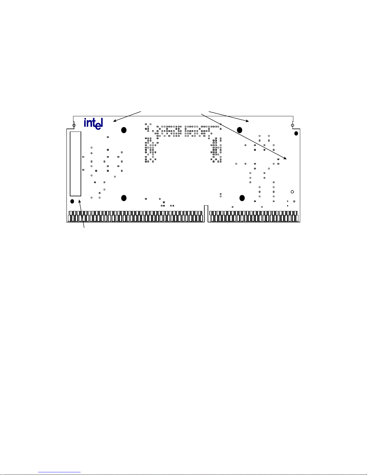
Intel® Celeron® Processor and Boxed Intel® Celeron® Processor
Markings (S.E.P. Package)
Static White Silkscreen marks
®
FFFFFFFF SYYYY
266/66 COA
Dynamic laser mark area
NOTES:
• SYYYY = S-spec Number.
FFFFFFFF = FPO # (Test Lot Traceability #).
•
COA = Country of Assembly.
celeron ™
i m ©’98
Page 10
INTEL® CELERON® PROCESSOR SPECIFICATION UPDATE
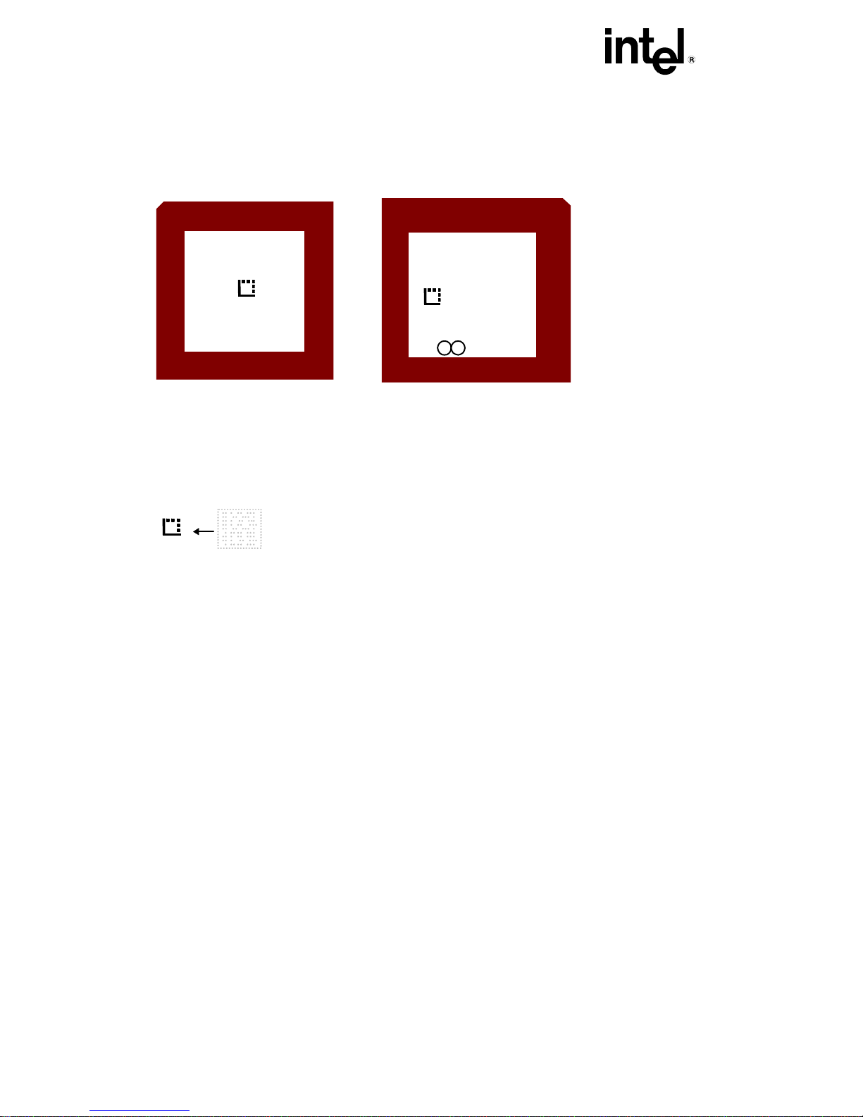
Intel® Celeron® Processor and Boxed Intel® Celeron® Processor
Markings (PPGA Package)
Top
Bottom
int l
e
celeron
AAAAAAAZZZ
LLL SYYYY
Country of Origin
FFFFFFFF-XXXX
M C
’98
i
®
TM
NOTES:
AAAAAAA = Product Code
ZZZ = Processor Speed (MHz)
LLL = Integrated Level-Two Cache Size (in Kilobytes)
SYYYY = S-Spec Number
FFFFFFFF-XXXX = Assembly Lot Tracking Number
2-D Matrix Mark
Intel UCC#
Order Code (Product - speed)
S Number
Lot Number (date, factory)
•
2
Page 11
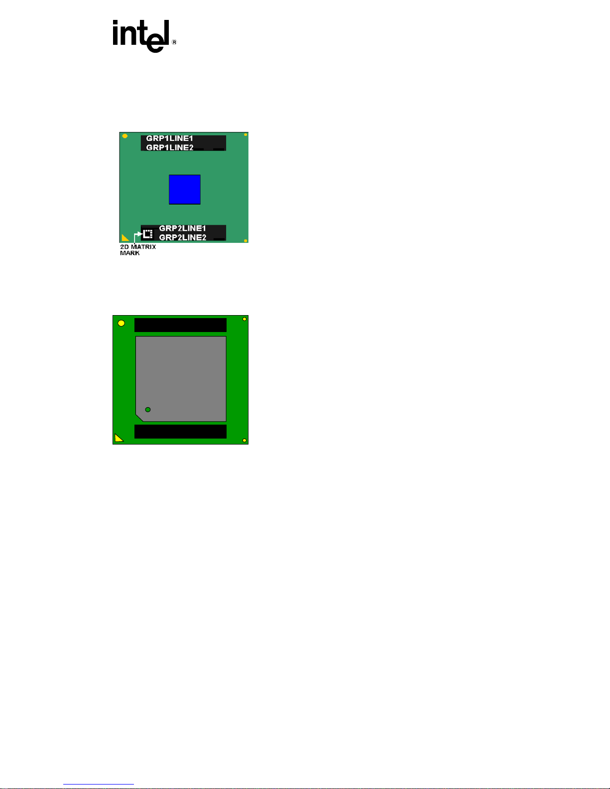
®
INTEL
CELERON® PROCESSOR SPECIFICATION UPDATE
Intel® Celeron® Processor and Boxed Intel® Celeron® Processor
Markings (FC-PGA/FC-PGA2 Package)
FC-PGA 370 Pin Package
GRP1LN1: INTEL (m)(c) '01_-_{COO}
GRP1LN2: {Core Freq}/{Cache}/{Bus Freq}/{Voltage}
GRP2LN1: {FPO}-{S/N}
GRP2LN2: CELERON {S-Spec}
FC-PGA2 370 Pin Package
GRP1LN1
GRP1LN2
GRP2LN1
GRP2LN2
GRP1LN1: INTEL (m)(c) '01_-_{Country of Origin}
GRP1LN2: {Core freq}/{Cache}/{Bus Freq}/{Voltage}
GRP2LN1: {FPO}-{S/N}
GRP2LN2: CELERON {S-Spec}
3
Page 12
INTEL® CELERON® PROCESSOR SPECIFICATION UPDATE
IDENTIFICATION INFORMATION
Complete identification information of the Celeron processor can be found in the Intel Processor Identification
and the CPUID Instruction
The Celeron processor can be identified by the following values:
Family1 Model2 Brand ID3
0110 0101 00h = Not Supported
0110 0110 00h = Not Supported
0110 1000 01h = “Intel® Celeron® Processor”
0110 10114 03h = “Intel® Celeron® Processor”
NOTES:
1. The Family corresponds to bits [11:8] of the EDX register after RESET, bits [11:8] of the EAX register after the CPUID
instruction is executed with a 1 in the EAX register, and the generation field of the Device ID register accessible
through Boundary Scan.
2. The Model corresponds to bits [7:4] of the EDX register after RESET, bits [7:4] of the EAX register after the CPUID
instruction is executed with a 1 in the EAX register, and the model field of the Device ID register accessible through
Boundary Scan.
3. The Brand ID corresponds to bits [7:0] of the EBX register after the CPUID instruction is executed with a 1 in the EAX
register.
4. This only applies to units with processor signature of 0x6B1.
The Celeron processor’s second level (L2) cache size can be determined by the following register contents:
0-Kbyte Unified L2 Cache1 40h
128-Kbyte Unified L2 Cache1 41h
256-Kbyte 8 way set associative 32byte line
NOTE:
1. When the EAX register contains a value of 2, the CPUID instruction loads the EAX, EBX, ECX and EDX registers with
descriptors that indicate the processors cache and TLB characteristics. The lower 8 bits of the EAX register (AL) contain
a value that identifies the number of times the CPUID has to be executed to obtain a complete image of the processor’s
caching systems. The remainder of the EAX register, the EBX, ECX and EDX registers contain the cache and TLB
descriptors. When bit 31 in a given register is zero, that register contains valid 8-bit descriptors. To decode descriptors,
move sequentially from the most significant byte of the register down through the least significant byte of the register.
Assuming bit 31 is 0, then that register contains valid cache or TLB descriptors in bits 24 through 31, bits 16 through 23,
bits 8 through 15 and bits 0 through 7. Software must compare the value contained in each of the descriptor bit fields
according to the definition of the CPUID instruction . For more details refer to the AP-485 Intel Processor Identification
and the CPUID Instruction Application Note.
application note (Document Number 241618).
1
size, L2 Cache
82h
4
Page 13

®
INTEL
S-Spec
Core
Stepping
Intel® Celeron® Processor Identification Information
L2 Cache
Size
(Kbytes)
CELERON® PROCESSOR SPECIFICATION UPDATE
Package
and
Revision
Notes
CPUID
Speed (MHz)
Core/Bus
SL2SY A0 0 0650h 266/66 SEPP Rev. 1
SL2YN A0 0 0650h 266/66 SEPP Rev. 1 1
SL2YP A0 0 0650h 300/66 SEPP Rev. 1
SL2Z7 A0 0 0650h 300/66 SEPP Rev. 1 1
SL2TR A1 0 0651h 266/66 SEPP Rev. 1
SL2QG A1 0 0651h 266/66 SEPP Rev. 1 1
SL2X8 A1 0 0651h 300/66 SEPP Rev. 1
SL2Y2 A1 0 0651h 300/66 SEPP Rev. 1 1
SL2Y3 B0 0 0652h 266/66
SL2Y4 B0 0 0652h 300/66
SL2WM A0 128 0660h 300A/66
SL32A A0 128 0660h 300A/66
SL2WN A0 128 0660h 333/66
SL32B A0 128 0660h 333/66
SEPP Rev. 1
SEPP Rev. 1
SEPP Rev. 1
SEPP Rev. 1
SEPP Rev. 1
SEPP Rev. 1
1
1
3
1
3
1
SL376 A0 128 0660h 366/66 SEPP Rev. 1
SL37Q A0 128 0660h 366/66 SEPP Rev. 1 1
SL39Z A0 128 0660h 400/66 SEPP Rev. 1
SL37V A0 128 0660h 400/66 SEPP Rev. 1 1
SL3BC A0 128 0660h 433/66 SEPP Rev. 1
SL39Z A0 128 0660h 400/66
SL37V A0 128 0660h 400/66
SL3BC A0 128 0660h 433/66
SL35Q B0 128 0665h 300A/66
PPGA
PPGA
PPGA
PPGA
SL35Q B0 128 0665h 300A/66 PPGA 2
SL36A B0 128 0665h 300A/66
PPGA
18
SL35R B0 128 0665h 333/66 PPGA 2
SL36B B0 128 0665h 333/66 PPGA
SL36C B0 128 0665h 366/66 PPGA
SL35S B0 128 0665h 366/66 PPGA 2
5
Page 14

INTEL® CELERON® PROCESSOR SPECIFICATION UPDATE
Intel® Celeron® Processor Identification Information
S-Spec
Core
Stepping
L2 Cache
Size
(Kbytes)
CPUID
Speed (MHz)
Core/Bus
Package
and
Revision
Notes
SL3A2 B0 128 0665h 400/66 PPGA
SL37X B0 128 0665h 400/66 PPGA 2
SL3BA B0 128 0665h 433/66 PPGA
SL3BS B0 128 0665h 433/66 PPGA 2
SL3EH B0 128 0665h 466/66 PPGA
SL3FL B0 128 0665h 466/66 PPGA 2
SL3FY B0 128 0665h 500/66 PPGA
SL3LQ B0 128 0665h 500/66 PPGA 2
SL3FZ B0 128 0665h 533/66 PPGA
SL3PZ B0 128 0665h 533/66 PPGA 2
SL46S B0 128 0683h 533A/66 FC-PGA
SL3W6 B0 128 0683h 533A/66 FC-PGA 2
SL46T B0 128 0683h 566/66 FC-PGA
SL3W7 B0 128 0683h 566/66 FC-PGA 2
SL4PC C0 128 0686h 566/66 FC-PGA 2, 7, 5
SL4NW
SL5L5
C0 128 0686h 566/66 FC-PGA 2, 7, 5
D0 128 068Ah 566/66 FC-PGA 7, 8
SL46U B0 128 0683h 600/66 FC-PGA
SL3W8 B0 128 0683h 600/66 FC-PGA 2
SL4PB
SL4NX
C0 128 0686h 600/66 FC-PGA 2, 7, 5
C0 128 0686h 600/66 FC-PGA 2, 7, 5
SL3VS B0 128 0683h 633/66 FC-PGA
SL3W9 B0 128 0683h 633/66 FC-PGA 2
SL4PA C0 128 0686h 633/66 FC-PGA 2, 6, 5
SL4NY C0 128 0686h 633/66 FC-PGA 2, 6, 5
SL48E B0 128 0683h 667/66 FC-PGA
SL4AB B0 128 0683h 667/66 FC-PGA 2
SL4P9 C0 128 0686h 667/66 FC-PGA 2, 6, 5
SL4NZ C0 128 0686h 667/66 FC-PGA 2, 6, 5
6
Page 15

®
INTEL
CELERON® PROCESSOR SPECIFICATION UPDATE
Intel® Celeron® Processor Identification Information
S-Spec
Core
Stepping
L2 Cache
Size
(Kbytes)
CPUID
Speed (MHz)
Core/Bus
Package
and
Revision
Notes
SL48F B0 128 0683h 700/66 FC-PGA
SL4EG B0 128 0683h 700/66 FC-PGA 2
SL4P8 C0 128 0686h 700/66 FC-PGA 2, 4, 5
SL4P2 C0 128 0686h 700/66 FC-PGA 2, 4, 5
SL4P7 C0 128 0686h 733/66 FC-PGA 4, 5
SL4P3 C0 128 0686h 733/66 FC-PGA 2, 4, 5
SL52Y D0 128 068Ah 733/66 FC-PGA 4, 8
SL5E9 D0 128 068Ah 733/66 FC-PGA 2, 4, 8
SL4P6 C0 128 0686h 766/66 FC-PGA 4, 5
SL4QF C0 128 0686h 766/66 FC-PGA 2, 4, 5
SL52X D0 128 068Ah 766/66 FC-PGA 4, 8
SL5EA D0 128 068Ah 766/66 FC-PGA 2, 4, 8
SL4TF C0 128 0686h 800/100 FC-PGA 4, 5
SL45R C0 128 0686h 800/100 FC-PGA 2, 4, 5
SL54P D0 128 068Ah 800/100 FC-PGA 4, 8
SL5WC D0 128 068Ah 800/100 FC-PGA 4, 8
SL5EB D0 128 068Ah 800/100 FC-PGA 2, 4, 8
SL5WW D0 128 068Ah 800/100 FC-PGA 2, 4, 8
SL5GA C0 128 0686h 850/100 FC-PGA 4, 5
SL5GB C0 128 0686h 850/100 FC-PGA 2, 4, 5
SL54Q D0 128 068Ah 850/100 FC-PGA 4, 8
SL5EC D0 128 068Ah 850/100 FC-PGA 2, 4, 8
SL5LX D0 128 068Ah 900/100 FC-PGA 8, 9
SL5WA D0 128 068Ah 900/100 FC-PGA 8, 9
SL5MQ D0 128
SL5WY D0 128
SL633 D0 128 068Ah 900/100 FC-PGA2
SL5UZ D0 128 068Ah 950/100 FC-PGA
068Ah 900/100 FC-PGA 2, 8, 9
068Ah 900/100 FC-PGA 2, 8, 9
2,8,14
8, 10
SL5V2 D0 128 068Ah 950/100 FC-PGA 2, 8, 10
7
Page 16

INTEL® CELERON® PROCESSOR SPECIFICATION UPDATE
Intel® Celeron® Processor Identification Information
S-Spec
Core
Stepping
L2 Cache
Size
(Kbytes)
CPUID
Speed (MHz)
Core/Bus
Package
and
Revision
SL634 D0 128 068Ah 950/100 FC-PGA2
Notes
2,8,14
8
Page 17

®
INTEL
S-Spec
Core
Stepping
Intel® Celeron® Processor Identification Information
L2 Cache
Size
(Kbytes)
CELERON® PROCESSOR SPECIFICATION UPDATE
Package
and
Revision
CPUID
Speed (MHz)
Core/Bus
SL5XT D0 128 068Ah 1 GHz/100 FC-PGA
SL5XQ D0 128 068Ah 1 GHz/100 FC-PGA 2, 8,11
SL5XU D0 128 068Ah 1.10
FC-PGA
GHz/100
SL5XR D0 128 068Ah 1.10
FC-PGA 2, 8,9
GHz/100
SL5VQ A1 256 06B1h 1.10A
FC-PGA2
GHz/100
SL5ZE A1 256 06B1h 1.10A
FC-PGA2
GHz/100
SL6CA B1 256 06B4h 1.10A
FC-PGA2 13, 15
GHz/100
SL6JR B1 256 06B4h 1.10A
FC-PGA2
GHz/100
SL5XS A1 256 06B1h 1.20
FC-PGA2
GHz/100
SL5Y5 A1 256 06B1h 1.20
FC-PGA2
GHz/100
SL656 A1 256 06B1h 1.20
FC-PGA2
GHz/100
SL68P A1 256 06B1h 1.20
FC-PGA2
GHz/100
SL6C8 B1 256 06B4h 1.20
FC-PGA2
GHz/100
SL6JS B1 256 06B4h 1.20
FC-PGA2
GHz/100
SL5VR A1 256 06B1h 1.30
FC-PGA2
GHz/100
SL5ZJ A1 256 06B1h 1.30
FC-PGA2
GHz/100
SL6C7 B1 256 06B4h 1.30
FC-PGA2
GHz/100
SL6JT B1 256 06B4h 1.30
FC-PGA2
GHz/100
SL64V A1 256 06B1h 1.40
FC-PGA2
GHz/100
SL68G A1 256 06B1h 1.40
FC-PGA2 2,14,15
GHz/100
Notes
8,11
8, 9
2,12,13
2,12,13
2,13, 15
12,13
2,12,13
15,17
2, 15, 17
15, 17
2,15, 17
15,16
2,15,16
15, 16
2,15, 16
14,15
9
Page 18

INTEL® CELERON® PROCESSOR SPECIFICATION UPDATE
Intel® Celeron® Processor Identification Information
L2 Cache
S-Spec
Core
Stepping
Size
(Kbytes)
CPUID
Speed (MHz)
Core/Bus
SL6C6 B1 256 06B4h 1.40
GHz/100
SL6JU B1 256 06B4h 1.40
GHz/100
SL6C5 B1 256 06B4h 1.50
GHz/100
SL6JV B1 256 06B4h 1.50
GHz/100
NOTES:
1. This is a boxed Celeron processor with an attached fan heatsink.
2. This is a boxed Celeron processor with an unattached fan heatsink.
3. This part also ships as a boxed Celeron processor with an attached fan heatsink.
4.
This part requires Tj of 80° C.
5. This part uses a V
6. This part will require Tj of 82C.
7. This part will require Tj of 90C.
8. This part uses a V
9.
This part has max Tj of 77° C.
10.
This part has max Tj of 79° C.
11.
This part has max Tj of 75° C.
12. This part uses a V
13. This part has max Tcase of 69 Deg C
14. This part has max Tcase of 72 Deg C
15. This part uses a V
16. This part has max Tcase of 71 Deg C
17. This part has max Tcase of 70 Deg C
18. This part has min Tcase of 5 deg C, max Tcase of 85 deg C and TDP of 17.8 W,
19. This part uses a V
CC
CORE
CC
CORE
CC
CORE
CC
CORE
CC
CORE
of 1.7 V.
of 1.75 V.
of 1.475 V.
of 1.5 V.
of 1.5V.
Package
and
Revision
FC-PGA2
FC-PGA2
Notes
14, 15
2,14, 15
FC-PGA2 1,3, 19
FC-PGA2 1,3, 19
10
Page 19

®
INTEL
CELERON® PROCESSOR SPECIFICATION UPDATE
SUMMARY OF CHANGES
The following table indicates the Errata, Documentation Changes, Specification Clarifications, or Specification Changes that
apply to Celeron processors. Intel intends to fix some of the errata in a future stepping of the component, and to account for
the other outstanding issues through documentation or specification changes as noted. This table uses the following
notations:
X:
Change applies to the given processor stepping.
(No mark) or (blank box): This item is fixed in or does not apply to the given stepping.
Doc: Document change or update that will be implemented.
PlanFix: This erratum may be fixed in a future stepping of the product.
Fixed: This erratum has been previously fixed.
NoFix: There are no plans to fix this erratum.
Doc: Intel intends to update the appropriate documentation in a future revision.
AP: APIC related erratum.
PKG: This column refers to errata on the Intel® Celeron® processor substrate.
Shaded: This item is either new or modified from the previous version of the document.
Each Specification Update item is prefixed with a capital letter to distinguish the product. The key below
Specification Change, Erratum, Specification Clarification, or Documentation
details the letters that are used in Intel’s microprocessor Specification Updates:
A = Dual-Core Intel
®
C = Intel
D = Dual-Core Intel
E = Intel
F = Intel
Celeron® processor
®
Pentium® III processor
®
Pentium® processor Extreme Edition and Intel® Pentium® D processor
I = Dual-Core Intel
J = 64-bit Intel
K = Mobile Intel
®
L = Intel
M = Mobile Intel
N = Intel
O = Intel
P = Intel
Celeron® D processor
®
Pentium® 4 processor
®
Xeon® processor MP
®
Xeon® processor
Q = Mobile Intel
technology
®
R = Intel
Pentium® 4 processor on 90 nm process
S = 64-bit Intel
T = Mobile Intel
U = 64-bit Intel
V = Mobile Intel
®
W= Intel
X = Intel
Y = Intel
Z = Mobile Intel
AA = Intel
AB = Intel
Celeron® M processor
®
Pentium® M processor on 90 nm process with 2 MB L2 Cache
®
Pentium® M processor
®
Pentium® D Processor 900 Sequence and Intel® Pentium® Processor Extreme Edition 955, 965
®
Pentium® 4 Processor 6x1 Sequence
®
Xeon® processor 7000 sequence
®
Xeon® Processor 2.80 GHz
®
Xeon® Processor
®
Xeon® processor MP with 1 MB L2 Cache
®
Pentium® III processor
®
Celeron® processor
®
Pentium® 4 processor supporting Hyper-Threading Technology on 90 nm process
®
Xeon® processor with 800 MHz system bus (1 MB and 2 MB L2 cache versions)
®
Pentium® 4 processor-M
®
Xeon® processor MP with up to 8 MB L3 Cache
®
Celeron® processor on .13 Micron Process in Micro-FCPGA Package
®
Pentium® 4 processor with 533 MHz system bus
11
Page 20

INTEL® CELERON® PROCESSOR SPECIFICATION UPDATE
®
AC = Intel
AD = Intel
AE = Intel
AF = Dual-Core Intel
AG = Dual-Core Intel
Celeron® Processor in 478 Pin Package
®
Celeron® D processor on 65 nm process
®
Core™ Duo Processor and Intel® Core™ Solo processor on 65 nm process
®
Xeon® processor LV
®
Xeon® Processor 5100 Series
AH = Intel® Core™2 Duo/Solo Processor for Intel® Centrino® Duo Processor
Technology
AI = Intel
AJ = Quad-Core Intel
AK = Intel
AL = Dual-Core Intel
AN = Intel
AO = Quad-Core Intel
AP = Dual-Core Intel
AQ = Intel
®
Core™2 Extreme Processor X6800Δ and Intel® Core™2 Duo Desktop Processor E6000Δ and
Δ
Sequence
E4000
®
Core™2 Extreme quad-core processor QX6700Δ and Intel® Core™2 Quad processor Q6600Δ
®
Pentium® Dual-Core Processor
®
Pentium® Dual-Core Desktop Processor E2000Δ Sequence
®
Xeon® Processor 5300 Series
®
Xeon® Processor 7100 Series
®
Xeon® processor 3200 series
®
Xeon® Processor 3000 Series
AR = Intel® Celeron processor 500 series
AS = Intel® Xeon® processor 7200, 7300 series
Summary of Errata
NO. CPUID/Stepping Plans ERRATA
650h
651h
660h
665h
683h
686h
68Ah
6B1h
6B4h
A0
A1
A0
B0
B0
C0
D0
A1
C1 X X X X X X X X X NoFix
B1
FP Data Operand Pointer
may be incorrectly calculated
after FP access which wraps
64-Kbyte boundary in 16-bit
code
C2 X X X X X X X X X NoFix Differences exist in debug
exception reporting
C3 X X X X X X X X X NoFix Code fetch matching
disabled debug register may
cause debug exception
C4 X X X X X X X X X NoFix FP inexact-result exception
flag may not be set
C5 X X X X X X X X X NoFix BTM for SMI will contain
incorrect FROM EIP
C6 X X X X X X X X X NoFix I/O restart in SMM may fail
after simultaneous MCE
C7 X X X X X X X X X NoFix Branch traps do not function
if BTMs are also enabled
C8 X X X X X X X X X NoFix Machine check exception
handler may not always
execute successfully
C9 X X X X X X X X X NoFix LBER may be corrupted after
some events
C10 X X X X X X X X X NoFix BTMs may be corrupted
during simultaneous L1
12
Page 21

®
INTEL
CELERON® PROCESSOR SPECIFICATION UPDATE
Summary of Errata
686h
68Ah
6B1h
6B4h
C0
D0
A1
B1
A0
651h
A1
660h
A0
665h
B0
683h
B0
NO. CPUID/Stepping Plans ERRATA
650h
cache line replacement
C11 X X X X Fixed Potential early deassertion of
LOCK# during split-lock
cycles
C12 X X X X Fixed A20M# may be inverted after
returning from and Reset
SMM
C13 X X Fixed Reporting of floating-point
exception may be delayed
C14 X X X X X X X X X NoFix Near CALL to ESP creates
unexpected EIP address
C15 X X Fixed Built-in self test always gives
nonzero result
C16 X X X X Fixed THERMTRIP# may not be
asserted as specified
C17 X Fixed Cache state corruption in the
presence of page A/D-bit
setting and snoop traffic
C18 X Fixed Snoop cycle generates
spurious machine check
exception
C19 X X Fixed MOVD/MOVQ instruction
writes to memory
prematurely
C20 X X X X X X X X X NoFix Memory type undefined for
nonmemory operations
C21 X X Fixed Bus protocol conflict with
optimized chipsets
C22 X X X X X X X X X NoFix FP Data Operand Pointer
may not be zero after power
on or Reset
C23 X X X X X X X X X NoFix MOVD following zeroing
instruction can cause
incorrect result
C24 X X X X X X X X X NoFix Premature execution of a
load operation prior to
exception handler invocation
C25 X X X X X X X X X NoFix Read portion of RMW
instruction may execute
twice
13
Page 22

INTEL® CELERON® PROCESSOR SPECIFICATION UPDATE
Summary of Errata
NO. CPUID/Stepping Plans ERRATA
650h
651h
660h
665h
683h
686h
68Ah
6B1h
6B4h
A0
A1
A0
B0
B0
C0
D0
A1
B1
C26 X X X X Fixed Test pin must be high during
power up
C27 X X X X X X X X Fixed Intervening writeback may
occur during locked
transaction
C28 X X X X X X X X X NoFix MC2_STATUS MSR has
model-specific error code
and machine check
architecture error code
reversed
C29 X X X X X X X X X NoFix MOV with debug register
causes debug exception
C30 X X X X X X X X X NoFix Upper four PAT entries not
usable with Mode B or Mode
C paging
C31 X X Fixed Incorrect memory type may
be used when MTRRs are
disabled
C32 X X X Fixed Misprediction in program
flow may cause unexpected
instruction execution
C33 X X X X X X X X X NoFix Data Breakpoint Exception in
a displacement relative near
call may corrupt EIP
C34 X X X X X X X X X NoFix System bus ECC not
functional with 2:1 ratio
C35 X X X X X X X Fixed Fault on REP CMPS/SCAS
operation may cause
incorrect EIP
C36 X X X X X X X NoFix RDMSR and WRMSR to
invalid MSR address may not
cause GP fault
C37 X X X X X X X NoFix SYSENTER/SYSEXIT
instructions can implicitly
load “null segment selector”
to SS and CS registers
C38 X X X X X X X NoFix PRELOAD followed by
EXTEST does not load
boundary scan data
C39 X X X X X X Fixed Far jump to new TSS with D-
bit cleared may cause
system hang
14
Page 23

®
INTEL
CELERON® PROCESSOR SPECIFICATION UPDATE
Summary of Errata
NO. CPUID/Stepping Plans ERRATA
650h
651h
660h
665h
683h
686h
68Ah
6B1h
6B4h
A0
A1
A0
B0
B0
C0
D0
A1
B1
C40 X X X X Fixed Incorrect chunk ordering may
prevent execution of the
machine check exception
handler after BINIT#
C41 X X X X X Fixed UC write may be reordered
around a cacheable write
C42 X X X X X X Fixed Resume Flag may not be
cleared after debug
exception
C43 X X X X Fixed Internal cache protocol
violation may cause system
hang
C44 X X X X X X X X X NoFix GP# fault on WRMSR to
ROB_CR_BKUPTMPDR6
C45 X X X X X Fixed Machine Check Exception
may occur due to improper
line eviction in the IFU
C46 X X X X X X X X X NoFix Lower bits of SMRAM
SMBASE register cannot be
written with an ITP
C47 X X X X X X Fixed Task switch may cause
wrong PTE and PDE access
bit to be set
C48 X X X X X X X X X NoFix Cross-modifying code
operations on a jump
instruction may cause a
general protection fault
C49 X X X X X X X Fixed Deadlock may occur due to
illegal-instruction/page-miss
combination
C50 X X X X X X X X X NoFix FLUSH# assertion following
STPCLK# may prevent CPU
clocks from stopping
C51 X X X X X X Fixed Floating-point exception
condition may be deferred
C52 X X X X X X X Fixed Cache Line Reads May
Result in Eviction of Invalid
Data
15
Page 24

INTEL® CELERON® PROCESSOR SPECIFICATION UPDATE
Summary of Errata
NO. CPUID/Stepping Plans ERRATA
650h
651h
660h
665h
683h
686h
68Ah
6B1h
6B4h
A0
A1
A0
B0
B0
C0
D0
A1
B1
C53 X X X X X NoFix FLUSH# servicing delayed
while waiting for
STARTUP_IPI in 2-way MP
systems
C54 X X X X X NoFix Double ECC error on read
may result in BINIT#
C55 X X X X X NoFix MCE due to L2 parity error
gives L1 MCACOD.LL
C56 X X X X X NoFix EFLAGS discrepancy on a
page fault after a
multiprocessor TLB
shootdown
C57 X X X X X NoFix Mixed cacheability of lock
variables is problematic in
MP systems
C58 X X X X X NoFix INT 1 with DR7.GD set does
not clear DR7.GD
C59 X X X X X NoFix Potential loss of data
coherency during MP data
ownership transfer
C60 X X X X X NoFix Misaligned Locked access to
APIC space results in a hang
C61 X X X X X NoFix Memory ordering based
synchronization may cause a
livelock condition in MP
Systems
C62 X X X X X NoFix Processor may assert
DRDY# on a write with no
data
C63 X Fixed Machine check exception
may occur due to improper
line eviction in the IFU
C65 X X NoFix Snoop request may cause
DBSY# hang
C66 X Fixed MASKMOVQ instruction
interaction with string
operation may cause
deadlock
C67 X X X X X NoFix MOVD, CVTSI2SS, or
PINSRW Following Zeroing
Instruction Can Cause
Incorrect Result
16
Page 25

®
INTEL
CELERON® PROCESSOR SPECIFICATION UPDATE
Summary of Errata
686h
68Ah
6B1h
6B4h
C0
D0
A1
B1
A0
651h
A1
660h
A0
665h
B0
683h
B0
NO. CPUID/Stepping Plans ERRATA
650h
C68 X NoFix Snoop probe during FLUSH#
could cause L2 to be left in
shared state
C69 X Fixed Livelock May Occur Due to
IFU Line Eviction
C70 X X X X X Fixed Selector for the LTR/LLDT
register may get corrupted
C71 X X X X X X X X X NoFix
INIT does not clear global
entries in the TLB
C72 X X X X X X X X X NoFix
VM bit will be cleared on a
double fault handler
C73 X X X X X X X X X NoFix
Memory aliasing with
inconsistent A and D bits
may cause processor
deadlock
C74 X X X X X X X X X
NoFix
Processor may report invalid
TSS fault instead of Double
fault during mode C paging
C75 X X Fixed APIC failure at CPU
core/system bus frequency
of 766/66 MHz
C76 X X X X X X X X X NoFix Machine check exception
may occur when interleaving
code between different
memory types
C77 X X X X X X X X X NoFix Wrong ESP Register Values
During a Fault in VM86 Mode
C78 X X X X X X X X X NoFix APIC ICR Write May Cause
Interrupt Not to be Sent
When ICR Delivery Bit
Pending
C79 X X X X X X X X Fixed The instruction fetch unit
(IFU) may fetch
instructions based upon stale
CR3 data after a write to
CR3 Register
C80 X NoFix Processor Might not Exit
Sleep State Properly Upon
De-assertion of CPUSLP#
Signal
C81 X X NoFix During Boundary Scan, BCLK
not Sampled High When
17
Page 26

INTEL® CELERON® PROCESSOR SPECIFICATION UPDATE
Summary of Errata
NO. CPUID/Stepping Plans ERRATA
650h
651h
660h
665h
683h
686h
68Ah
6B1h
6B4h
A0
A1
A0
B0
B0
C0
D0
A1
B1
SLP# is Asserted Low
C82 X X
NoFix Incorrect assertion of
THERMTRIP# Signal
C83 X X X X X X X X X NoFix Under some complex
conditions, the Instructions in
the shadow of a JMP FAR
may be unintentionally
executed and retired
C84 X X X X X X X X X NoFix Processor Does not Flag #GP
on Non-zero Write to Certain
MSRs
C85 X X X X X X X X X NoFix
C86 X X X X X X X X X NoFix
IFU/BSU Deadlock May
Cause System Hang
REP MOVS Operation in Fast
string Mode Continues in that
Mode When Crossing into a
Page with a Different Memory
Type
C87 X X X X X X X X X NoFix
POPF and POPFD
Instructions that Set the Trap
Flag Bit May Cause
Unpredictable Processor
Behavior
C88 X X X X X X X X X NoFix
The FXSAVE, STOS, or
MOVS Instruction May Cause
a Store Ordering Violation
When Data Crosses a Page
with a UC Memory Type
C89 X X X X X X X X X NoFix
Code Segment Limit Violation
May Occur on 4 Gigabyte
Limit Check
C90 X X X X X X X X X NoFix
FST Instruction with Numeric
and Null Segment Exceptions
May Cause General Protection
Faults to be Missed and FP
Linear Address (FLA)
Mismatch
C91 X X X X X X X X X NoFix
Code Segment (CS) is
Incorrect on SMM Handler
when SMBASE is not Aligned
C92 X X X X X X X X X NoFix
Page with PAT (Page Attribute
Table) Set to USWC
(Uncacheable Speculative
Write Combine) While
Associated MTRR (Memory
Type Range Register) is UC
18
Page 27

®
INTEL
CELERON® PROCESSOR SPECIFICATION UPDATE
Summary of Errata
686h
68Ah
6B1h
6B4h
C0
D0
A1
B1
A0
651h
A1
660h
A0
665h
B0
683h
B0
NO. CPUID/Stepping Plans ERRATA
650h
(Uncacheable) May
Consolidate to UC
C93 X X X X X X X X X NoFix
Under Certain Conditions LTR
(Load Task Register)
Instruction May Result in
System Hang
C93 X X X X X X X X X NoFix
Under Certain Conditions LTR
(Load Task Register)
Instruction May Result in
System Hang
C94 X X X X X X X X X NoFix
Loading from Memory Type
USWC (Uncacheable
Speculative Write Combine)
May Get Its Data Internally
Forwarded from a Previous
Pending Store
C95 X X X X X X X X X NoFix
FXSAVE after FNINIT Without
an Intervening FP (Floating
Point) Instruction May Save
Uninitialized Values for FDP
(x87 FPU Instruction Operand
(Data) Pointer Offset) and
FDS (x87 FPU Instruction
Operand (Data) Pointer
Selector)
C96 X X X X X X X X X NoFix
FSTP (Floating Point
Store) Instruction Under
Certain Conditions May Result
In Erroneously Setting a Valid
Bit on an FP (Floating
Point) Stack Register
C97 X X X X X X X X X NoFix
Invalid Entries in PageDirectory-Pointer-Table
Register (PDPTR) May Cause
General Protection (#GP)
Exception if the Reserved Bits
are Set to One
Writing the Local Vector
Table (LVT)
C98 X X X X X X X X X NoFix
when an Interrupt is Pending
May Cause an Unexpected
Interrupt
The Processor May Report
C99 X X X X X X X X X NoFix
an Invalid TSS Fault Instead
of a #GP Fault
C100 X X X X X X X X X NoFix
A Write to an APIC Register
Sometimes May Appear to
19
Page 28

INTEL® CELERON® PROCESSOR SPECIFICATION UPDATE
Summary of Errata
NO. CPUID/Stepping Plans ERRATA
650h
651h
660h
665h
683h
686h
68Ah
6B1h
6B4h
A0
A1
A0
B0
B0
C0
D0
A1
B1
Have Not Occurred
Using 2M/4M Pages When
C101 X X X X X X X X X NoFix
A20M# Is Asserted May
Result in Incorrect Address
Translations
Values for LBR/BTS/BTM will
C102 X X X X X X X X X NoFix
be Incorrect after an Exit
from SMM
C103 X X X X X X X X X NoFix
INIT Does Not Clear Global
Entries in the TLB
REP MOVS/STOS Executing
with Fast Strings Enabled
and Crossing Page
C104 X X X X X X X X X NoFix
Boundaries with Inconsistent
Memory Types may use an
Incorrect Data Size or Lead
to Memory-Ordering
Violations
The BS Flag in DR6 May be
C105 X X X X X X X X X NoFix
Set for Non-Single-Step #DB
Exception
Fault on ENTER Instruction
C106 X X X X X X X X X NoFix
May Result in Unexpected
Values on Stack Frame
Unaligned Accesses to
C107 X X X X X X X X X NoFix
Paging Structures May
Cause the Processor to
Hang
INVLPG Operation for Large
C108 X X X X X X X X X NoFix
(2M/4M) Pages May be
Incomplete under Certain
Conditions
Page Access Bit May be Set
C109 X X X X X X X X X NoFix
Prior to Signaling a Code
Segment Limit Fault
EFLAGS, CR0, CR4 and the
C110 X X X X X X X X X NoFix
EXF4 Signal May be
Incorrect after Shutdown
Performance Monitoring
Event
C111 X X X X X X X X X NoFix
FP_MMX_TRANS_TO_MMX
May Not Count Some
Transitions
20
Page 29

®
INTEL
CELERON® PROCESSOR SPECIFICATION UPDATE
* Fix will be only on Celeron
processors with CPUID=068xh.
Summary of Documentation Changes
CPUID/Stepping
NO.
650h
A0
651h
A1
660h
A0
665h
B0
683h
B0
686h
C0
68Ah
D0
6B1h
A1
6B4h
B1
Plans
DOCUMENTATION
CHANGES
C1 X X X X X X X X X Doc SSE and SSE2 Instructions
Opcodes
C2
X X X X X X X X X Doc
Executing the SSE2 Variant
on a Non-SSE2 Capable
Processor
C3 X X X X X X X X X Doc
C4 X X X X X X X X X Doc
C5 X X X X X X X X X Doc
Direction Flag (DF) Mistakenly
Denoted as a System Flag
Fopcode Compatibility Mode
FCOS, FPTAN, FSIN, and
FSINCOS Trigonometric
Domain not correct
C6 X X X X X X X X X Doc
C7 X X X X X X X X X Doc
C8 X X X X X X X X X Doc
C9 X X X X X X X X X Doc
C10 X X X X X X X X X Doc
C11 X X X X X X X X X Doc
C12 X X X X X X X X X Doc
C13 X X X X X X X X X Doc
C14 X X X X X X X X X Doc
C15 X X X X X X X X X Doc
C16 X X X X X X X X X Doc
C17 X X X X X X X X X Doc
C18 X X X X X X X X X Doc
Incorrect Description of stack
EFLAGS Register Correction
PSE-36 Paging Mechanism
0x33 Opcode
Incorrect Information for SLDT
LGDT/LIDT Instruction
Information Correction
Errors In Instruction Set
Reference
RSM Instruction Set Summary
Correct MOVAPS and
MOVAPD Operand Section
DAA—Decimal Adjust AL after
Addition
DAS—Decimal Adjust AL after
Subtraction
Omission of Dependency
between BTM and LBR
I/O Permissions Bitmap Base
Addy > 0xDFFF Does not
Cause #GP(0) Fault
C19 X X X X X X X X X Doc
C20 X X X X X X X X X Doc
C21 X X X X X X X X X Doc
Wrong Field Width for MINSS
and MAXSS
Figure 15-12 PEBS Record
Format
I/O Permission Bit Map
21
Page 30

INTEL® CELERON® PROCESSOR SPECIFICATION UPDATE
Summary of Documentation Changes
CPUID/Stepping
650h
651h
660h
665h
683h
686h
68Ah
6B1h
NO.
A0
A1
A0
B0
B0
C0
D0
A1
6B4h
B1
Plans
C22 X X X X X X X X X Doc
C23 X X X X X X X X X Doc
C24 X X X X X X X X X Doc
DOCUMENTATION
CHANGES
Cache Description
Instruction Formats and
Encoding
Machine-Check Initialization
22
Page 31

®
INTEL
CELERON® PROCESSOR SPECIFICATION UPDATE
Summary of Specification Clarifications
CPUID/Stepping
NO.
650h
A0
651h
A1
660h
A0
665h
B0
683h
B0
686h
C0
68Ah
D0
6B1h
A1
6B4h
B1
Plans
SPECIFICATION
CLARIFICATIONS
C1 X X X X X X X X X Doc PWRGOOD inactive pulse
width
C2 X X X X X X X X X Doc Floating-point opcode
clarification
C3 X X X X X X X X X Doc MTRR initialization
clarification
C4 X X X X X X X X X Doc Non-AGTL+ output low
current clarification
23
Page 32

INTEL® CELERON® PROCESSOR SPECIFICATION UPDATE
Summary of Specification Changes
NO.
650h
A0
651h
A1
660h
A0
CPUID/Stepping
665h
683h
B0
B0
686h
C0
68Ah
D0
6B1h
A1
6B4h
B1
Plans
SPECIFICATION
CHANGES
C1 X X X X X X X X X Doc RESET# pin definition
C2 X X X Doc Tco max revision for
533A,566 & 600MHz
C3 X X X X X Doc Processor thermal
specification change and
TDP redefined
24
Page 33

®
INTEL
CELERON® PROCESSOR SPECIFICATION UPDATE
ERRATA
C1. FP Data Operand Pointer May Be Incorrectly Calculated After
FP Access Which Wraps 64-Kbyte Boundary in 16-Bit Code
Problem: The FP Data Operand Pointer is the effective address of the operand associated with the last
noncontrol floating-point instruction executed by the machine. If an 80-bit floating-point access (load or store)
occurs in a 16-bit mode other than protected mode (in which case the access will produce a segment limit
violation), the memory access wraps a 64-Kbyte boundary, and the floating-point environment is subsequently
saved, the value contained in the FP Data Operand Pointer may be incorrect.
Implication:
the following conditions:
• The operating system is using a segment greater than 64 Kbytes in size.
• An application is running in a 16-bit mode other than protected mode.
• An 80-bit floating-point load or store which wraps the 64-Kbyte boundary is executed.
• The operating system performs a floating-point environment store (FSAVE/FNSAVE/FSTENV/FNSTENV)
after the above memory access.
• The operating system uses the value contained in the FP Data Operand Pointer.
Wrapping an 80-bit floating-point load around a segment boundary in this way is not a normal programming
practice. Intel has not currently identified any software which exhibits this behavior.
A 32-bit operating system running 16-bit floating-point code may encounter this erratum, under
Workaround: If the FP Data Operand Pointer is used in an OS which may run 16-bit floating-point code,
care must be taken to ensure that no 80-bit floating-point accesses are wrapped around a 64-Kbyte boundary.
Status: For the steppings affected see the Summary of Changes at the beginning of this section.
C2. Differences Exist in Debug Exception Reporting
Problem: There exist some differences in the reporting of code and data breakpoint matches between that
specified by previous Celeron processor specifications and the behavior of Celeron processor, as described
below:
Case 1: The first case is for a breakpoint set on a MOVSS or POPSS instruction, when the instruction
following it causes a debug register protection fault (DR7.gd is already set, enabling the fault). The Celeron
processor reports delayed data breakpoint matches from the MOVSS or POPSS instructions by setting the
matching DR6.bi bits, along with the debug register protection fault (DR6.bd). If additional breakpoint faults
are matched during the call of the debug fault handler, the Celeron processor sets the breakpoint match bits
(DR6.bi) to reflect the breakpoints matched by both the MOVSS or POPSS breakpoint and the debug fault
handler call. The Celeron processor only sets DR6.bd in either situation, and does not set any of the DR6.bi
bits.
Case 2: In the second breakpoint reporting failure case, if a MOVSS or POPSS instruction with a data
breakpoint is followed by a store to memory which:
a) crosses a 4-Kbyte page boundary,
OR
25
Page 34

INTEL® CELERON® PROCESSOR SPECIFICATION UPDATE
b) causes the page table Access or Dirty (A/D) bits to be modified,
the breakpoint information for the MOVSS or POPSS will be lost. Previous Celeron processors retain this
information under these boundary conditions.
Case 3: If they occur after a MOVSS or POPSS instruction, the INTn, INTO, and INT3 instructions zero the
DR6.bi bits (bits B0 through B3), clearing pending breakpoint information, unlike previous In Celeron
processors.
Case 4: If a data breakpoint and an SMI (System Management Interrupt) occur simultaneously, the SMI will
be serviced via a call to the SMM handler, and the pending breakpoint will be lost.
Case 5: When an instruction that accesses a debug register is executed, and a breakpoint is encountered on
the instruction, the breakpoint is reported twice.
Case 6: Unlike previous versions of Intel Architecture processors, Celeron processors will not set the Bi bits
for a matching disabled breakpoint unless at least one other breakpoint is enabled.
Implication: When debugging or when developing debuggers for a Pentium III processor-based system, this
behavior should be noted. Normal usage of the MOVSS or POPSS instructions (i.e., following them with a
MOV ESP) will not exhibit the behavior of cases 1-3. Debugging in conjunction with SMM will be limited by
case 4.
Workaround: Following MOVSS and POPSS instructions with a MOV ESP instruction when using
breakpoints will avoid the first three cases of this erratum. No workaround has been identified for cases 4 or 5.
Status: For the steppings affected see the Summary of Changes at the beginning of this section.
C3. Code Fetch Matching Disabled Debug Register May Cause
Debug Exception
Problem: The bits L0-3 and G0-3 enable breakpoints local to a task and global to all tasks, respectively. If
one of these bits is set, a breakpoint is enabled, corresponding to the addresses in the debug registers DR0DR3. If at least one of these breakpoints is enabled, any of these registers are
0), and RW
instruction fetch will not cause an instruction-breakpoint fault based on a match with the address in the
disabled register(s). However, if the address in a disabled register matches the address of a code fetch which
also results in a page fault, an instruction-breakpoint fault will occur.
Implication:
breakpoint registers are not cleared when they are disabled. Debug software which does not implement a
code breakpoint handler will fail, if this occurs. If a handler is present, the fault will be serviced. Mixing data
and code may exacerbate this problem by allowing disabled data breakpoint registers to break on an
instruction fetch.
n for the disabled register is 00 (indicating a breakpoint on instruction execution), normally an
While debugging software, extraneous instruction-breakpoint faults may be encountered if
disabled (i.e., Ln and Gn are
Workaround: The debug handler should clear breakpoint registers before they become disabled.
Status: For the steppings affected see the Summary of Changes at the beginning of this section.
26
Page 35

®
INTEL
CELERON® PROCESSOR SPECIFICATION UPDATE
C4. FP Inexact-Result Exception Flag May Not Be Set
Problem: When the result of a floating-point operation is not exactly representable in the destination format
(1/3 in binary form, for example), an inexact-result (precision) exception occurs. When this occurs, the PE bit
(bit 5 of the FPU status word) is normally set by the processor. Under certain rare conditions, this bit may not
be set when this rounding occurs. However, other actions taken by the processor (invoking the software
exception handler if the exception is unmasked) are not affected. This erratum can only occur if the floatingpoint operation which causes the precision exception is immediately followed by one of the following
instructions:
• FST m32real
• FST m64real
• FSTP m32real
• FSTP m64real
• FSTP m80real
• FIST m16int
• FIST m32int
• FISTP m16int
• FISTP m32int
• FISTP m64int
Note that even if this combination of instructions is encountered, there is also a dependency on the internal
pipelining and execution state of both instructions in the processor.
Implication:
frequently, and produces a rounded result acceptable to most applications. The PE bit of the FPU status word
may not always be set upon receiving an inexact-result exception. Thus, if these exceptions are unmasked, a
floating-point error exception handler may not recognize that a precision exception occurred. Note that this is
a “sticky” bit, i.e., once set by an inexact-result condition, it remains set until cleared by software.
Inexact-result exceptions are commonly masked or ignored by applications, as it happens
Workaround: This condition can be avoided by inserting two NOP instructions between the two floating-
point instructions.
Status: For the steppings affected see the Summary of Changes at the beginning of this section.
C5. BTM for SMI Will Contain Incorrect FROM EIP
Problem: A system management interrupt (SMI) will produce a Branch Trace Message (BTM), if BTMs are
enabled. However, the FROM EIP field of the BTM (used to determine the address of the instruction which
was being executed when the SMI was serviced) will not have been updated for the SMI, so the field will
report the same FROM EIP as the previous BTM.
Implication:
usefulness of BTMs for debugging software in conjunction with System Management Mode (SMM).
A BTM which is issued for an SMI will not contain the correct FROM EIP, limiting the
Workaround: None identified
Status: For the steppings affected see the Summary of Changes at the beginning of this section.
27
Page 36

INTEL® CELERON® PROCESSOR SPECIFICATION UPDATE
C6. I/O Restart in SMM May Fail After Simultaneous MCE
Problem: If an I/O instruction (IN, INS, REP INS, OUT, OUTS, or REP OUTS) is being executed, and if the
data for this instruction becomes corrupted, the Celeron processor will signal a machine check exception
(MCE). If the instruction is directed at a device which is powered down, the processor may also receive an
assertion of SMI#. Since MCEs have higher priority, the processor will call the MCE handler, and the SMI#
assertion will remain pending. However, upon attempting to execute the first instruction of the MCE handler,
the SMI# will be recognized and the processor will attempt to execute the SMM handler. If the SMM handler is
completed successfully, it will attempt to restart the I/O instruction, but will not have the correct machine state,
due to the call to the MCE handler.
Implication:
SMM handler may attempt to restart such an I/O instruction, but will have corrupted state due to the MCE
handler call, leading to failure of the restart and shutdown of the processor.
A simultaneous MCE and SMI# assertion may occur for one of the I/O instructions above. The
Workaround: If a system implementation must support both SMM and MCEs, the first thing the SMM
handler code (when an I/O restart is to be performed) should do is check for a pending MCE. If there is an
MCE pending, the SMM handler should immediately exit via an RSM instruction and allow the machine check
exception handler to execute. If there is not, the SMM handler may proceed with its normal operation.
Status: For the steppings affected see the Summary of Changes at the beginning of this section.
C7. Branch Traps Do Not Function If BTMs Are Also Enabled
Problem: If branch traps or branch trace messages (BTMs) are enabled alone, both function as expected.
However, if both are enabled, only the BTMs will function, and the branch traps will be ignored.
Implication:
The branch traps and branch trace message debugging features cannot be used together.
Workaround: If branch trap functionality is desired, BTMs must be disabled.
Status: For the steppings affected see the Summary of Changes at the beginning of this section.
C8. Machine Check Exception Handler May Not Always Execute
Successfully
Problem: An asynchronous machine check exception (MCE), such as a BINIT# event, which occurs during
an access that splits a 4-Kbyte page boundary may leave some internal registers in an indeterminate state.
Thus, MCE handler code may not always run successfully if an asynchronous MCE has occurred previously.
Implication:
asynchronous MCEs usually occur upon detection of a catastrophic system condition that would also hang the
processor. Leaving MCEs disabled will result in the condition which caused the asynchronous MCE instead
causing the processor to enter shutdown. Therefore, leaving MCEs disabled may not improve overall system
behavior.
An MCE may not always result in the successful execution of the MCE handler. However,
Workaround: No workaround which would guarantee successful MCE handler execution under this
condition has been identified.
Status: For the steppings affected see the Summary of Changes at the beginning of this section.
28
Page 37

®
INTEL
CELERON® PROCESSOR SPECIFICATION UPDATE
C9. LBER May Be Corrupted After Some Events
Problem: The last branch record (LBR) and the last branch before exception record (LBER) can be used to
determine the source and destination information for previous branches or exceptions. The LBR contains the
source and destination addresses for the last branch or exception, and the LBER contains similar information
for the last branch taken before the last exception. This information is typically used to determine the location
of a branch which leads to execution of code which causes an exception. However, after a catastrophic bus
condition which results in an assertion of BINIT# and the re-initialization of the buses, the value in the LBER
may be corrupted. Also, after either a CALL which results in a fault or a software interrupt, the LBER and LBR
will be updated to the same value, when the LBER should not have been updated.
Implication:
occurs, the LBER will not contain reliable address information. The value of LBER should be used with caution
when debugging branching code; if the values in the LBR and LBER are the same, then the LBER value is
incorrect. Also, the value in the LBER should not be relied upon after a BINIT# event.
The LBER and LBR registers are used only for debugging purposes. When this erratum
Workaround: None identified
Status: For the steppings affected see the Summary of Changes at the beginning of this section.
C10. BTMs May Be Corrupted During Simultaneous L1 Cache Line
Replacement
Problem: When Branch Trace Messages (BTMs) are enabled and such a message is generated, the BTM
may be corrupted when issued to the bus by the L1 cache if a new line of data is brought into the L1 data
cache simultaneously. Though the new line being stored in the L1 cache is stored correctly, and no corruption
occurs in the data, the information in the BTM may be incorrect due to the internal collision of the data line and
the BTM.
Implication:
this boundary condition to occur have only been exhibited during focused simulation testing. Intel has currently
not observed this erratum in a system level validation environment.
Workaround: None identified
Status: For the steppings affected see the Summary of Changes at the beginning of this section.
Although BTMs may not be entirely reliable due to this erratum, the conditions necessary for
29
Page 38

INTEL® CELERON® PROCESSOR SPECIFICATION UPDATE
C11. Potential Early Deassertion of LOCK# During Split-Lock
Cycles
Problem: During a split-lock cycle there are four bus transactions: 1st ADS# (a partial read), 2nd ADS# (a
partial read), 3rd ADS# (a partial write), and the 4th ADS# (a partial write). Due to this erratum, LOCK# may
deassert one clock after the 4th ADS# of the split-lock cycle instead of after the 4th RS# assertion
corresponding to the 4th ADS# has been sampled. The following sequence of events are required for this
erratum to occur:
1. A lock cycle occurs (split or nonsplit).
2. Five more bus transactions (assertion of ADS#) occur.
3. A split-lock cycle occurs and BNR# toggles after the 3rd ADS# (partial write) of the split-lock cycle. This in
turn delays the assertion of the 4th ADS# of the split-lock cycle. BNR# toggling at this time could most
likely happen when the bus is set for an IOQ depth of 2.
When all of these events occur, LOCK# will be deasserted in the next clock after the 4th ADS# of the split-lock
cycle.
Implication:
This may affect chipset logic which monitors the behavior of LOCK# deassertion.
Workaround: None identified
Status: For the steppings affected see the Summary of Changes at the beginning of this section.
C12. A20M# May Be Inverted After Returning From SMM and
Reset
Problem: This erratum is seen when software causes the following events to occur:
1. The assertion of A20M# in real address mode.
2. After entering the 1-Mbyte address wrap-around mode caused by the assertion of A20M#, there is an
assertion of SMI# intended to cause a Reset or remove power to the processor. Once in the SMM
handler, software saves the SMM state save map to an area of nonvolatile memory from which it can be
restored at some point in the future. Then software asserts RESET# or removes power to the processor.
3. After exiting Reset or completion of power-on, software asserts SMI# again. Once in the SMM handler, it
then retrieves the old SMM state save map which was saved in event 2 above and copies it into the
current SMM state save map. Software then asserts A20M# and executes the RSM instruction. After
exiting the SMM handler, the polarity of A20M# is inverted.
Implication:
the 1-Mbyte address wrap-around mode is enabled when A20M# is deasserted, and does not occur when
A20M# is asserted).
If this erratum occurs, A20M# will behave with a polarity opposite from what is expected (i.e.,
Workaround: Software should save the A20M# signal state in nonvolatile memory before an assertion of
RESET# or a power down condition. After coming out of Reset or at power on, SMI# should be asserted
again. During the restoration of the old SMM state save map described in event 3 above, the entire map
should be restored, except for bit 5 of the byte at offset 7F18h. This bit should retain the value assigned to it
when the SMM state save map was created in event 3. The SMM handler should then restore the original
value of the A20M# signal.
30
Page 39

®
INTEL
CELERON® PROCESSOR SPECIFICATION UPDATE
Status: For the steppings affected see the Summary of Changes at the beginning of this section.
C13. Reporting of Floating-Point Exception May Be Delayed
Problem: The Celeron processor normally reports a floating-point exception for an instruction when the next
floating-point or Intel
interrupt corresponding to the exception may be delayed until the floating-point or MMX technology instruction
after the one which is expected to trigger the exception, if the following conditions are met:
1. A floating-point instruction causes an exception.
2. Before another floating-point or MMX technology instruction, any one of the following occurs:
• A subsequent data access occurs to a page which has not been marked as accessed
• Data is referenced which crosses a page boundary
• A possible page-fault condition is detected which, when resolved, completes without faulting
3. The instruction causing event 2 above is followed by a MOVQ or MOVD store instruction.
Implication:
Software which requires floating-point exceptions to be visible on the next floating-point or MMX technology
instruction, and which uses floating-point calculations on data which is then used for MMX technology
instructions, may see a delay in the reporting of a floating-point instruction exception in some cases. Note that
mixing floating-point and MMX technology instructions in this way is not recommended.
®
MMX™ technology instruction is executed. The assertion of FERR# and/or the INT 16
This erratum only affects software which operates with floating-point exceptions unmasked.
Workaround: Inserting a WAIT or FWAIT instruction (or reading the floating-point status register) between
the floating-point instruction and the MOVQ or MOVD instruction will give the expected results. This is already
the recommended practice for software.
Status: For the steppings affected see the Summary of Changes at the beginning of this section.
C14. Near CALL to ESP Creates Unexpected EIP Address
Problem: As documented, the CALL instruction saves procedure linking information in the procedure stack
and jumps to the called procedure specified with the destination (target) operand. The target operand
specifies the address of the first instruction in the called procedure. This operand can be an immediate value,
a general purpose register, or a memory location. When accessing an absolute address indirectly using the
stack pointer (ESP) as a base register, the base value used is the value in the ESP register before the
instruction executes. However, when accessing an absolute address directly using ESP as the base register,
the base value used is the value of ESP
register
before the instruction executed.
Implication:
unpredictable, depending on the particular application, and can range from no effect to the unexpected
termination of the application due to an exception. Intel has observed this erratum only in a focused testing
environment. Intel has not observed any commercially available operating system, application, or compiler
that makes use of or generates this instruction.
Due to this erratum, the processor may transfer control to an unintended address. Results are
Workaround: If the other seven general purpose registers are unavailable for use, and it is necessary to do
a CALL via the ESP register, first push ESP onto the stack, then perform an
CALL [ESP]). The saved version of ESP should be popped off the stack after the call returns.
Status: For the steppings affected see the Summary of Changes at the beginning of this section.
after the return value is pushed on the stack, not the value in the ESP
indirect call using ESP (e.g.,
31
Page 40

INTEL® CELERON® PROCESSOR SPECIFICATION UPDATE
C15. Built-in Self Test Always Gives Nonzero Result
Problem: The Built-in Self Test (BIST) of the Celeron processor does not give a zero result to indicate a
passing test. Regardless of pass or fail status, bit 6 of the BIST result in the EAX register after running BIST is
set.
Implication:
Software which relies on a zero result to indicate a passing BIST will indicate BIST failure.
Workaround: Mask bit 6 of the BIST result register when analyzing BIST results.
Status: For the steppings affected see the Summary of Changes at the beginning of this section.
C16. THERMTRIP# May Not Be Asserted as Specified
Problem: THERMTRIP# is a signal on the Celeron processor which is asserted when the core reaches a
critical temperature during operation as detailed in the processor specification. The Celeron processor may
not assert THERMTRIP# until a much higher temperature than the one specified is reached.
Implication:
can only occur when the processor is running with a T
75° C.
The THERMTRIP# feature is not functional on the Celeron processor. Note that this erratum
temperature over the maximum specification of
PLATE
Workaround: Avoid operation of the Celeron processor outside of the thermal specifications defined by the
processor specifications.
Status: For the steppings affected see the Summary of Changes at the beginning of this section.
C17. Cache State Corruption in the Presence of Page A/D-bit
Setting and Snoop Traffic
Problem: If an operating system uses the Page Access and/or Dirty bit feature implemented in the Intel
architecture and there is a significant amount of snoop traffic on the bus, while the processor is setting the
Access and/or Dirty bit the processor may inappropriately change a single L1 cache line to the modified state.
Implication:
errors, data corruption (with no parity error), unexpected application or operating system termination, or
system hangs.
Workaround: It is possible for BIOS code to contain a workaround for this erratum.
Status: For the steppings affected see the Summary of Changes at the beginning of this section.
32
The occurrence of this erratum may result in cache incoherency, which may cause parity
Page 41

®
INTEL
CELERON® PROCESSOR SPECIFICATION UPDATE
C18. Snoop Cycle Generates Spurious Machine Check Exception
Problem: The processor may incorrectly generate a Machine Check Exception (MCE) when it processes a
snoop access that does not hit the L1 data cache. Due to an internal logic error, this type of snoop cycle may
still check data parity on undriven data lines. The processor generates a spurious machine check exception as
a result of this unnecessary parity check.
Implication:
Check Exception reporting is enabled in the operating system.
A spurious machine check exception may result in an unexpected system halt if Machine
Workaround: It is possible for BIOS code to contain a workaround for this erratum. This workaround would
fix the erratum, however, the reporting of the data parity error will continue.
Status: For the steppings affected see the Summary of Changes at the beginning of this section.
C19. MOVD/MOVQ Instruction Writes to Memory Prematurely
Problem: When an instruction encounters a fault, the faulting instruction should not modify any CPU or
system state. However, when the MMX™ technology store instructions MOVD and MOVQ encounter any of
the following events, it is possible for the store to be committed to memory even though it should be canceled:
1. If CR0.EM = 1 (Emulation bit), then the store could happen prior to the triggered invalid opcode
exception.
2. If the floating-point Top-of-Stack (FP TOS) is not zero, then the store could happen prior to executing the
processor assist routine that sets the FP TOS to zero.
3. If there is an unmasked floating-point exception pending, then the store could happen prior to the
triggered unmasked floating-point exception.
4. If CR0.TS = 1 (Task Switched bit), then the store could happen prior to the triggered Device Not
Available (DNA) exception.
If the MOVD/MOVQ instruction is restarted after handling any of the above events, then the store will be
performed again, overwriting with the expected data. The instruction will not be restarted after event 1. The
instruction will definitely be restarted after events 2 and 4. The instruction may or may not be restarted after
event 3, depending on the specific exception handler.
Implication:
used to manipulate semaphores for multiprocessor synchronization, or if these MMX instructions are used to
write to uncacheable memory or memory mapped I/O that has side effects, e.g., graphics devices. This
erratum is completely transparent to all applications that do not have these characteristics. When each of the
above conditions are analyzed:
1. Setting the CR0.EM bit forces all floating-point/MMX instructions to be handled by software emulation.
The MOVD/MOVQ instruction, which is an MMX instruction, would be considered an invalid instruction.
Operating systems typically terminates the application after getting the expected invalid opcode fault.
2. The FP TOS not equal to 0 case only occurs when the MOVD/MOVQ store is the first MMX instruction in
an MMX technology routine and the previous floating-point routine did not clean up the floating-point
states properly when it exited. Floating-point routines commonly leave TOS to 0 prior to exiting. For a
store to be executed as the first MMX instruction in an MMX technology routine following a floating-point
routine, the software would be implementing instruction level intermixing of floating-point and MMX
instructions. Intel does not recommend this practice.
This erratum causes unpredictable behavior in an application if MOVD/MOVQ instructions are
33
Page 42

INTEL® CELERON® PROCESSOR SPECIFICATION UPDATE
3. The unmasked floating-point exception case only occurs if the store is the first MMX technology instruction
in an MMX technology routine and the previous floating-point routine exited with an unmasked floatingpoint exception pending. Again, for a store to be executed as the first MMX instruction in an MMX
technology routine following a floating-point routine, the software would be implementing instruction level
intermixing of floating-point and MMX instructions. Intel does not recommend this practice.
Device Not Available (DNA) exceptions occur naturally when a task switch is made between two tasks that
use either floating-point instructions and/or MMX instructions. For this erratum, in the event of the DNA
exception, data from the prior task may be temporarily stored to the present task’s program state.
Workaround: Do not use MMX instructions to manipulate semaphores for multiprocessor synchronization.
Do not use MOVD/MOVQ instructions to write directly to I/O devices if doing so triggers user visible side
effects. An OS can prevent old data from being stored to a new task’s program state by cleansing the FPU
explicitly after every task switch. Follow Intel’s recommended programming paradigms in the
Developer’s Optimization Manual
and MMX instructions. When transitioning to new a MMX technology routine, begin with an instruction that
does not depend on the prior state of either the MMX technology registers or the floating-point registers, such
as a load or PXOR mm0, mm0. Be sure that the FP TOS is clear before using MMX instructions.
for writing MMX technology programs. Specifically, do not mix floating-point
Intel Architecture
Status: For the steppings affected see the Summary of Changes at the beginning of this section.
C20. Memory Type Undefined for Nonmemory Operations
Problem: The Memory Type field for nonmemory transactions such as I/O and Special Cycles are
undefined. Although the Memory Type attribute for nonmemory operations logically should (and usually does)
manifest itself as UC, this feature is not designed into the implementation and is therefore inconsistent.
Implication:
Bus agents may decode a non-UC memory type for nonmemory bus transactions.
Workaround: Bus agents must consider transaction type to determine the validity of the Memory Type field
for a transaction.
Status: For the steppings affected see the Summary of Changes at the beginning of this section.
C21. Bus Protocol Conflict With Optimized Chipsets
Problem: A “dead” turnaround cycle with no agent driving the address, address parity, request command, or
request parity signals must occur between the processor driving these signals and the chipset driving them
after asserting BPRI#. The Celeron processor does not follow this protocol. Thus, if a system uses a chipset
or third party agent which optimizes its arbitration latency (reducing it to 2 clocks when it observes an active
(low) ADS# signal and an inactive (high) LOCK# signal on the same clock that BPRI# is asserted (driven
low)), the Celeron processor may cause bus contention during an unlocked bus exchange.
Implication:
cause a system-level setup timing violation on the address, address parity, request command, or request
parity signals on the system bus. This may result in a system hang or assertion of the AERR# signal, causing
an attempted corrective action or shutdown of the system, as the system hardware and software dictate. The
possibility of failure due to the contention caused by this erratum may be increased due to the processor’s
internal active pull-up of these signals on the clock after the signals are no longer being driven by the
processor.
34
This violation of the bus exchange protocol when using a reduced arbitration latency may
Page 43

®
INTEL
CELERON® PROCESSOR SPECIFICATION UPDATE
Workaround: If the chipset and third party agents used with the Celeron processor do not optimize their
arbitration latency as described above, no action is required. For the 66 MHz Celeron processor, no action is
required.
Status: For the steppings affected see the Summary of Changes at the beginning of this section.
C22. FP Data Operand Pointer May Not Be Zero After Power On or
Reset
Problem: The FP Data Operand Pointer, as specified, should be reset to zero upon power on or Reset by
the processor. Due to this erratum, the FP Data Operand Pointer may be nonzero after power on or Reset.
Implication:
power on or Reset without first executing an FINIT/FNINIT instruction will use an incorrect value, resulting in
incorrect behavior of the software.
Software which uses the FP Data Operand Pointer and count on its value being zero after
Workaround: Software should follow the recommendation in Section 8.2 of the Intel Architecture Software
Developer’s Manual, Volume 3: System Programming Guide
states that if the FPU will be used, software-initialization code should execute an FINIT/FNINIT instruction
following a hardware reset. This will correctly clear the FP Data Operand Pointer to zero.
(Order Number 243192). This recommendation
Status: For the steppings affected see the Summary of Changes at the beginning of this section.
35
Page 44

INTEL® CELERON® PROCESSOR SPECIFICATION UPDATE
C23. MOVD Following Zeroing Instruction Can Cause Incorrect
Result
Problem: An incorrect result may be calculated after the following circumstances occur:
1. A register has been zeroed with either a SUB reg, reg instruction or an XOR reg, reg instruction,
2. A value is moved with sign extension into the same register’s lower 16 bits; or a signed integer multiply is
performed to the same register’s lower 16 bits,
3. This register is then copied to an MMX™ technology register using the MOVD instruction prior to any
other operations on the sign-extended value.
Specifically, the sign may be incorrectly extended into bits 16-31 of the MMX technology register. Only the
MMX technology register is affected by this erratum.
The erratum only occurs when the 3 following steps occur in the order shown. The erratum may occur with up
to 40 intervening instructions that do not modify the sign-extended value between steps 2 and 3.
1. XOR EAX, EAX
or SUB EAX, EAX
2. MOVSX AX, BL
or MOVSX AX, byte ptr <memory address> or MOVSX AX, BX
or MOVSX AX, word ptr <memory address> or IMUL BL (AX implicit, opcode F6 /5)
or IMUL byte ptr <memory address> (AX implicit, opcode F6 /5) or IMUL AX, BX (opcode 0F AF /r)
or IMUL AX, word ptr <memory address> (opcode 0F AF /r) or IMUL AX, BX, 16 (opcode 6B /r ib)
or IMUL AX, word ptr <memory address>, 16 (opcode 6B /r ib) or IMUL AX, 8 (opcode 6B /r ib)
or IMUL AX, BX, 1024 (opcode 69 /r iw)
or IMUL AX, word ptr <memory address>, 1024 (opcode 69 /r iw) or IMUL AX, 1024 (opcode 69 /r iw)
or CBW
3. MOVD MM0, EAX
Note that the values for immediate byte/words are merely representative (i.e., 8, 16, 1024) and that any value
in the range for the size may be affected. Also, note that this erratum may occur with “EAX” replaced with any
32-bit general purpose register, and “AX” with the corresponding 16-bit version of that replacement. “BL” or
“BX” can be replaced with any 8-bit or 16-bit general purpose register. The CBW and IMUL (opcode F6 /5)
instructions are specific to the EAX register only.
In the example, EAX is forced to contain 0 by the XOR or SUB instructions. Since the four types of the
MOVSX or IMUL instructions and the CBW instruction modify only bits 15:8 of EAX by sign extending the
lower 8 bits of EAX, bits 31:16 of EAX should always contain 0. This implies that when MOVD copies EAX to
MM0, bits 31:16 of MM0 should also be 0. Under certain scenarios, bits 31:16 of MM0 are not 0, but are
replicas of bit 15 (the 16th bit) of AX. This is noticeable when the value in AX after the MOVSX, IMUL or CBW
instruction is negative, i.e., bit 15 of AX is a 1.
When AX is positive (bit 15 of AX is a 0), MOVD will always produce the correct answer. If AX is negative (bit
15 of AX is a 1), MOVD may produce the right answer or the wrong answer depending on the point in time
when the MOVD instruction is executed in relation to the MOVSX, IMUL or CBW instruction.
Implication:
discarding the incorrect bits, to an application failure. If the MMX technology-enabled application in which
MOVD is used to manipulate pixels, it is possible for one or more pixels to exhibit the wrong color or position
momentarily. It is also possible for a computational application that uses the MOVD instruction in the manner
described above to produce incorrect data. Note that this data may cause an unexpected page fault or general
protection fault.
The effect of incorrect execution will vary from unnoticeable, due to the code sequence
36
Page 45

®
INTEL
CELERON® PROCESSOR SPECIFICATION UPDATE
Workaround: There are two possible workarounds for this erratum:
1. Rather than using the MOVSX-MOVD or CBW-MOVD pairing to handle one variable at a time, use the
sign extension capabilities (PSRAW, etc.) within MMX technology for operating on multiple variables. This
would result in higher performance as well.
2. Insert another operation that modifies or copies the sign-extended value between the MOVSX/IMUL/CBW
instruction and the MOVD instruction as in the example below:
XOR EAX, EAX (or SUB EAX, EAX)
MOVSX AX, BL (or other MOVSX, other IMUL or CBW instruction)
*MOV EAX, EAX
MOVD MM0, EAX
*Note: MOV EAX, EAX is used here as it is fairly generic. Again, EAX can be any 32-bit register.
Status: For the steppings affected see the Summary of Changes at the beginning of this section.
C24. Premature Execution of a Load Operation Prior to Exception
Handler Invocation
Problem: This erratum can occur with any of the following situations:
1. If an instruction that performs a memory load causes a code segment limit violation
2. If a waiting floating-point instruction or MMX™ instruction that performs a memory load has a floating-
point exception pending
3. If an MMX instruction that performs a memory load and has either CR0.EM =1 (Emulation bit set), or a
floating-point Top-of-Stack (FP TOS) not equal to 0, or a DNA exception pending
If any of the above circumstances occur, it is possible that the load portion of the instruction will have
executed before the exception handler is entered.
Implication:
is no impact from the load being prematurely executed, nor from the restart and subsequent re-execution of
that instruction by the exception handler. If the target of the load is to uncached memory that has a system
side effect, restarting the instruction may cause unexpected system behavior due to the repetition of the side
effect.
In normal code execution where the target of the load operation is to write back memory there
Workaround: Code which performs loads from memory that has side-effects can effectively workaround this
behavior by using simple integer-based load instructions when accessing side-effect memory and by ensuring
that all code is written such that a code segment limit violation cannot occur as a part of reading from sideeffect memory.
Status: For the steppings affected see the Summary of Changes at the beginning of this section.
37
Page 46

INTEL® CELERON® PROCESSOR SPECIFICATION UPDATE
C25. Read Portion of RMW Instruction May Execute Twice
Problem: When the Celeron processor executes a read-modify-write (RMW) arithmetic instruction, with
memory as the destination, it is possible for a page fault to occur during the execution of the store on the
memory operand after the read operation has completed but before the write operation completes.
If the memory targeted for the instruction is UC (uncached), memory will observe the occurrence of the initial
load before the page fault handler and again if the instruction is restarted.
Implication:
If, however, the load targets a memory region that has side-effects, multiple occurrences of the initial load may
lead to unpredictable system behavior.
This erratum has no effect if the memory targeted for the RMW instruction has no side-effects.
Workaround: Hardware and software developers who write device drivers for custom hardware that may
have a side-effect style of design should use simple loads and simple stores to transfer data to and from the
device. Then the memory location will simply be read twice with no additional implications.
Status: For the steppings affected see the Summary of Changes at the beginning of this section.
C26. Test Pin Must Be High During Power Up
Problem: The Celeron processor uses the PWRGOOD signal to ensure that no voltage sequencing issues
arise; no pin assertions should cause the processor to change its behavior until this signal is asserted, when
all power supplies and clocks to the processor are valid and stable. However, if the TESTHI signal is at a low
voltage level when the core power supply comes up, it will cause the processor to enter an invalid test state.
Implication:
Workaround: Ensure that the 2.5 V (V
plane. If 2.5 V ramps after core, pull up TESTHI to 2.5 V (V
up will keep the signal from being asserted during power up. For new motherboard designs, it is
recommended that TESTHI be pulled up to 2.0 V (V
If this erratum occurs, the system may boot normally however, L2 cache may not be initialized.
) power supply ramps at or before the 2.0 V (V
CC
2.5
CC
CORE
) with a 100K Ohm resistor. The internal pull-
CC
2.5
) using a 1K-10K Ohm resistor.
CC
CORE
) power
Status: For the steppings affected see the Summary of Changes at the beginning of this section.
C27. Intervening Writeback May Occur During Locked Transaction
Problem: During a transaction which has the LOCK# signal asserted (i.e., a locked transaction), there is a
potential for an explicit writeback caused by a previous transaction to complete while the bus is locked. The
explicit writeback will only be issued by the processor which has locked the bus, and the lock signal will not be
deasserted until the locked transaction completes, but the atomicity of a lock may be compromised by this
erratum. Note that the explicit writeback is an expected cycle, and no memory ordering violations will occur.
This erratum is, however, a violation of the bus lock protocol.
Implication:
transactions may only consist of a read-write or read-read-write-write locked sequence, with no transactions
intervening, may lose synchronization of state due to the intervening explicit writeback. Systems using
chipsets or TPAs which can accept the intervening transaction will not be affected.
A chipset or third-party agent (TPA) which tracks bus transactions in such a way that locked
Workaround: The bus tracking logic of all devices on the system bus should allow for the occurrence of an
intervening transaction during a locked transaction.
38
Page 47

®
INTEL
CELERON® PROCESSOR SPECIFICATION UPDATE
Status: For the steppings affected see the Summary of Changes at the beginning of this section.
C28. MC2_STATUS MSR Has Model-Specific Error Code and
Machine Check Architecture Error Code Reversed
Problem: The Intel Architecture Software Developer’s Manual, Volume 3: System Programming Guide,
documents that for the MC
code fields and bits 31:16 contain the model-specific error code field. However, for the MC2_STATUS MSR,
these bits have been reversed. For the MC2_STATUS MSR, bits 15:0 contain the model-specific error code
field and bits 31:16 contain the MCA error code field.
Implication:
is not taken into account.
A machine check error may be decoded incorrectly if this erratum on the MC2_STATUS MSR
i_STATUS MSR, bits 15:0 contain the MCA (machine-check architecture) error
Workaround: When decoding the MC2_STATUS MSR, reverse the two error fields.
Status: For the steppings affected see the Summary of Changes at the beginning of this section.
C29. MOV With Debug Register Causes Debug Exception
Problem: When in V86 mode, if a MOV instruction is executed on debug registers, a general-protection
exception (#GP) should be generated, as documented in the
Volume 3: System Programming Guide
flag (GD) bit is set, the observed behavior is that a debug exception (#DB) is generated instead.
Implication:
MOV on debug registers in V86 mode, a debug exception will be generated instead of the expected generalprotection fault.
With debug-register protection enabled (i.e., the GD bit set), when attempting to execute a
, Section 15.2. However, in the case when the general detect enable
Workaround: In general, operating systems do not set the GD bit when they are in V86 mode. The GD bit is
generally set and used by debuggers. The debug exception handler should check that the exception did not
occur in V86 mode before continuing. If the exception did occur in V86 mode, the exception may be directed
to the general-protection exception handler.
Status: For the steppings affected see the Summary of Changes at the beginning of this section.
Intel Architecture Software Developer's Manual,
39
Page 48

INTEL® CELERON® PROCESSOR SPECIFICATION UPDATE
C30. Upper Four PAT Entries Not Usable With Mode B or Mode C
Paging
Problem: The Page Attribute Table (PAT) contains eight entries, which must all be initialized and considered
when setting up memory types for the Celeron processor. However, in Mode B or Mode C paging, the upper
four entries do not function correctly for 4-Kbyte pages. Specifically, bit seven of page table entries that
translate addresses to 4-Kbyte pages should be used as the upper bit of a three-bit index to determine the
PAT entry that specifies the memory type for the page. When Mode B (CR4.PSE = 1) and/or Mode C
(CR4.PAE) are enabled, the processor forces this bit to zero when determining the memory type regardless of
the value in the page table entry. The upper four entries of the PAT function correctly for 2-Mbyte and 4-Mbyte
large pages (specified by bit 12 of the page directory entry for those translations).
Implication:
used. In Mode A paging (4-Kbyte pages only), all eight entries may be used. All eight entries may be used for
large pages in Mode B or C paging.
Only the lower four PAT entries are useful for 4-Kbyte translations when Mode B or C paging is
Workaround: None identified
Status: For the steppings affected see the Summary of Changes at the beginning of this section.
C31. Incorrect Memory Type May Be Used When MTRRs Are
Disabled
Problem: If the Memory Type Range Registers (MTRRs) are disabled without setting the CR0.CD bit to
disable caching, and the Page Attribute Table (PAT) entries are left in their default setting, which includes
UC- memory type (PCD = 1, PWT = 0; see the
System Programming Guide,
writeback (WB). Also, if the page tables are set to a memory type other than UC-, then the effective memory
type used will be that specified by the page tables and PAT. Any regions of memory normally forced to UC by
the MTRRs (such as the VGA video region) may now be incorrectly cached and speculatively accessed.
Even if the CR0.CD bit is correctly set when the MTRRs are disabled and the PAT is left in its default state,
then retries and out of order retirement of UC accesses may occur, contrary to the strong ordering expected
for these transactions.
Implication:
processor behavior when running with the MTRRs disabled. Interaction between the mouse, cursor, and VGA
video display leading to video corruption may occur as a symptom of this erratum as well.
The occurrence of this erratum may result in the use of incorrect data and unpredictable
for details), data for entries set to UC- will be cached as if the memory type were
Workaround: Ensure that when the MTRRs are disabled, the CR0.CD bit is set to disable caching. This
recommendation is described in
Programming Guide
CR0.CD bit, flushing the caches, and disabling the MTRRs to ensure that UC memory type is always returned
and strong ordering is maintained.
. If it is necessary to disable the MTRRs, first clear the PAT register before setting the
Intel Architecture Software Developer’s Manual, Volume 3: System
Status: For the steppings affected see the Summary of Changes at the beginning of this section.
Intel Architecture Software Developer’s Manual, Volume 3:
40
Page 49

®
INTEL
CELERON® PROCESSOR SPECIFICATION UPDATE
C32. Misprediction in Program Flow May Cause Unexpected
Instruction Execution
Problem: To optimize performance through dynamic execution technology, the P6 architecture has the
ability to predict program flow. In the event of a misprediction, the processor will normally clear the incorrect
prediction, adjust the EIP to the correct location, and flush out any instructions it may have fetched from the
misprediction. In circumstances where a branch misprediction occurs, the correct target of the branch has
already been opportunistically fetched into the streaming buffers, and the L2 cycle caused by the evicted
cache line is retried by the L2 cache, the processor may fail to flush out the retirement unit before the
speculative program flow is committed to a permanent state.
Implication:
Manifestations of this failure may result in:
• Unexpected values in EIP
• Faults or traps (e.g., page faults) on instructions that do not normally cause faults
• Faults in the middle of instructions
• Unexplained values in registers/memory at the correct EIP
The results of this erratum may range from no effect to unpredictable application or OS failure.
Workaround: It is possible for BIOS code to contain a workaround for this erratum.
Status: For the steppings affected see the Summary of Changes at the beginning of this section.
C33. Data Breakpoint Exception in a Displacement Relative Near
Call May Corrupt EIP
Problem: If a misaligned data breakpoint is programmed to the same cache line as the memory location
where the stack push of a near call is performed and any data breakpoints are enabled, the processor will
update the stack and ESP appropriately, but may skip the code at the destination of the call. Hence, program
execution will continue with the next instruction immediately following the call, instead of the target of the call.
Implication: The failure mechanism for this erratum is that the call would not be taken; therefore,
instructions in the called subroutine would not be executed. As a result, any code relying on the execution of
the subroutine will behave unpredictably.
Workaround: Whether enabled or not, do not program a misaligned data breakpoint to the same cache line
on the stack where the push for the near call is performed.
Status: For the stepping affected see the Summary of Changes at the beginning of this section.
C34. System Bus ECC Not Functional With 2:1 Ratio
Problem: If a processor is underclocked at a core frequency to system bus frequency ratio of 2:1 and
system bus ECC is enabled, the system bus ECC detection and correction will negatively affect internal timing
dependencies.
Implication:
may behave unpredictably due to these timing dependencies.
If system bus ECC is enabled, and the processor is underclocked at a 2:1 ratio, the system
41
Page 50

INTEL® CELERON® PROCESSOR SPECIFICATION UPDATE
Workaround: All bus agents that support system bus ECC must disable it when a 2:1 ratio is used.
Status: For the steppings affected see the Summary of Changes at the beginning of this section.
C35. Fault on REP CMPS/SCAS Operation May Cause Incorrect
EIP
Problem: If either a General Protection Fault, Alignment Check Fault or Machine Check Exception occur
during the first iteration of a REP CMPS or a REP SCAS instruction, an incorrect EIP may be pushed onto the
stack of the event handler if all the following conditions are true:
• The event occurs on the initial load performed by the instruction(s)
• The condition of the zero flag before the repeat instruction happens to be opposite of the repeat condition
(i.e., REP/REPE/REPZ CMPS/SCAS with ZF = 0 or RENE/REPNZ CMPS/SCAS with ZF = 1)
• The faulting micro-op and a particular micro-op of the REP instruction are retired in the retirement unit in
a specific sequence
The EIP will point to the instruction following the REP CMPS/SCAS instead of pointing to the faulting
instruction.
Implication: The result of the incorrect EIP may range from no effect to unexpected application/OS
behavior.
Workaround: None identified
Status: For the steppings affected see the Summary of Changes at the beginning of this section.
C36. RDMSR or WRMSR To Invalid MSR Address May Not Cause
GP Fault
Problem: The RDMSR and WRMSR instructions allow reading or writing of MSRs (Model Specific
Registers) based on the index number placed in ECX. The processor should reject access to any reserved or
unimplemented MSRs by generating #GP(0). However, there are some invalid MSR addresses for which the
processor will not generate #GP(0).
Implication: For RDMSR, undefined values will be read into EDX:EAX. For WRMSR, undefined processor
behavior may result.
Workaround: Do not use invalid MSR addresses with RDMSR or WRMSR.
Status: For the steppings affected see the Summary of Changes at the beginning of this section.
42
Page 51

®
INTEL
CELERON® PROCESSOR SPECIFICATION UPDATE
C37. SYSENTER/SYSEXIT Instructions Can Implicitly Load “Null
Segment Selector” to SS and CS Registers
Problem: According to the processor specification, attempting to load a null segment selector into the CS
and SS segment registers should generate a General Protection Fault (#GP). Although loading a null segment
selector to the other segment registers is allowed, the processor will generate an exception when the segment
register holding a null selector is used to access memory.
However, the SYSENTER instruction can implicitly load a null value to the SS segment selector. This can
occur if the value in SYSENTER_CS_MSR is between FFF8h and FFFBh when the SYSENTER instruction is
executed. This behavior is part of the SYSENTER/SYSEXIT instruction definition; the content of the
SYSTEM_CS_MSR is always incremented by 8 before it is loaded into the SS. This operation will set the null
bit in the segment selector if a null result is generated, but it does not generate a #GP on the SYSENTER
instruction itself. An exception will be generated as expected when the SS register is used to access memory,
however.
The SYSEXIT instruction will also exhibit this behavior for both CS and SS when executed with the value in
SYSENTER_CS_MSR between FFF0h and FFF3h, or between FFE8h and FFEBh.
Implication: These instructions are intended for operating system use. If this erratum occurs (and the OS
does not ensure that the processor never has a null segment selector in the SS or CS segment registers), the
processor’s behavior may become unpredictable, possibly resulting in system failure.
Workaround: Do not initialize the SYSTEM_CS_MSR with the values between FFF8h and FFFBh, FFF0h
and FFF3h, or FFE8h and FFEBh before executing SYSENTER or SYSEXIT.
Status: For the steppings affected see the Summary of Changes at the beginning of this section.
C38. PRELOAD Followed by EXTEST Does Not Load Boundary
Scan Data
Problem: According to the IEEE 1149.1 Standard, the EXTEST instruction would use data “typically loaded
onto the latched parallel outputs of boundary-scan shift-register stages using the SAMPLE/PRELOAD
instruction prior to the selection of the EXTEST instruction.” As a result of this erratum, this method cannot be
used to load the data onto the outputs.
Implication: Using the PRELOAD instruction prior to the EXTEST instruction will not produce expected data
after the completion of EXTEST.
Workaround: None identified
Status: For the steppings affected see the Summary of Changes at the beginning of this section.
43
Page 52

INTEL® CELERON® PROCESSOR SPECIFICATION UPDATE
C39. Far Jump to New TSS With D-bit Cleared May Cause System
Hang
Problem: A task switch may be performed by executing a far jump through a task gate or to a new Task
State Segment (TSS) directly. Normally, when such a jump to a new TSS occurs, the D-bit (which indicates
that the page referenced by a Page Table Entry (PTE) has been modified) for the PTE which maps the
location of the previous TSS will already be set and the processor will operate as expected. However, if the Dbit is clear at the time of the jump to the new TSS, the processor will hang.
Implication: If an OS is used which can clear the D-bit for system pages, and which jumps to a new TSS on
a task switch, then a condition may occur which results in a system hang. Intel has not identified any
commercial software which may encounter this condition; this erratum was discovered in a focused testing
environment.
Workaround: Ensure that OS code does not clear the D-bit for system pages (including any pages that
contain a task gate or TSS). Use task gates rather than jumping to a new TSS when performing a task switch.
Status: For the steppings affected see the Summary of Changes at the beginning of this section.
C40. Incorrect Chunk Ordering May Prevent Execution of the
Machine Check Exception Handler After BINIT#
Problem: If a catastrophic bus error is detected which results in a BINIT# assertion, and the BINIT#
assertion is propagated to the processor’s L2 cache at the same time that data is being sent to the processor,
then the data may become corrupted in the processor’s L1 cache.
Implication: Since BINIT# assertion is due to a catastrophic event on the bus, the corrupted data will not be
used. However, it may prevent the processor from executing the Machine Check Exception (MCE) handler,
causing the system to hang.
Workaround: None identified
Status: For the steppings affected see the Summary of Changes at the beginning of this section.
44
Page 53

®
INTEL
CELERON® PROCESSOR SPECIFICATION UPDATE
C41. UC Write May Be Reordered Around a Cacheable Write
Problem: After a write occurs to a UC (uncacheable) region of memory, there exists a small window of
opportunity where a subsequent write transaction targeted for a UC memory region may be reordered in front
of a write targeted to a region of cacheable memory. This erratum can only occur during the following
sequence of bus transactions:
1. A write to memory mapped as UC occurs
2. A write to memory mapped as cacheable (WB or WT) which is present in Shared or Invalid state in the
L2 cache occurs
3. During the bus snoop of the cacheable line, another store to UC memory occurs
Implication: If this erratum occurs, the second UC write will be observed on the bus prior to the Bus
Invalidate Line (BIL) or Bus Read Invalidate Line (BRIL) transaction for the cacheable write. This presents a
small window of opportunity for a fast bus-mastering I/O device which triggers an action based on the second
UC write to arbitrate and gain ownership of the bus prior to the completion of the cacheable write, possibly
retrieving stale data.
Workaround: It is possible for BIOS code to contain a workaround for this erratum.
Status: For the steppings affected see the Summary of Changes at the beginning of this section.
C42. Resume Flag May Not Be Cleared After Debug Exception
Problem: The Resume Flag (RF) is normally cleared by the processor after executing an instruction which
causes a debug exception (#DB). In the process of determining whether the RF needs to be cleared after
executing the instruction, the processor uses an internal register containing stale data. The stale data may
unpredictably prevent the processor from clearing the RF.
Implication: If this erratum occurs, further debug exceptions will be disabled.
Workaround: None identified
Status: For the steppings affected see the Summary of Changes at the beginning of this section.
45
Page 54

INTEL® CELERON® PROCESSOR SPECIFICATION UPDATE
C43. Internal Cache Protocol Violation May Cause System Hang
Problem: A Celeron processor-based system may hang due to an internal cache protocol violation. During
multiple transactions targeted at the same cacheline, there exists a small window of time such that the
processor's internal timings align to create a livelock situation. The scenario, which results in the erratum, is
summarized below:
Scenario:
1. A snoopable transaction is issued to address A. This snoopable transaction can be issued by the
processor or the chipset.
2. The snoopable transaction hits a modified line in the processor’s L1 data cache.
3. The processor issues two code fetches from the L2 cache before the snoopable transaction reaches the
top of the In-Order Queue and before the snoopable transaction's modified L1 cache line containing
address A is brought out on the system bus.
At the same time, a locked access to the L1 cache occurs.
Implication: A Celeron processor may cause a system to hang if the above listed sequence of events occur.
The probability of encountering this erratum increases with I/O queue depth greater than four.
Workaround: It is possible for the BIOS code to contain a workaround for this erratum.
Status: For the steppings affected see the Summary of Changes at the beginning of this section.
C44. GP# Fault on WRMSR to ROB_CR_BKUPTMPDR6
Problem: Writing a ‘1’ to unimplemented bit(s) in the ROB_CR_BKUPTMPDR6 MSR (offset 1E0h) will result
in a general protection fault (GP#).
Implication: The normal process used to write an MSR is to read the MSR using RDMSR, modify the bit(s)
of interest, and then to write the MSR using WRMSR. Because of this erratum, this process may result in a
GP# fault when used to modify the ROB_CR_BKUPTMPDR6 MSR.
Workaround: When writing to ROB_CR_BKUPTMPDR6 all unimplemented bits must be ‘0.’ Implemented
bits may be set as ‘0’ or ‘1’ as desired.
Status: For the steppings affected see the Summary of Changes at the beginning of this section.
46
Page 55

®
INTEL
CELERON® PROCESSOR SPECIFICATION UPDATE
C45. Machine Check Exception May Occur Due to Improper Line
Eviction in the IFU
Problem: The Celeron processor is designed to signal an unrecoverable Machine Check Exception (MCE)
as a consistency checking mechanism. Under a complex set of circumstances involving multiple speculative
branches and memory accesses there exists a one cycle long window in which the processor may signal a
MCE in the Instruction Fetch Unit (IFU) because instructions previously decoded have been evicted from the
IFU. The one cycle long window is opened when an opportunistic fetch receives a partial hit on a previously
executed but not as yet completed store resident in the store buffer. The resulting partial hit erroneously
causes the eviction of a line from the IFU at a time when the processor is expecting the line to still be present.
If the MCE for this particular IFU event is disabled, execution will continue normally.
Implication: Since the probability of this erratum occurring increases with the number of processors, the risk
is lower on Celeron processor-based systems as they do not have multi-processor support. If this erratum
does occur, a machine check exception will result. Note systems that implement an operating system that
does not enable the Machine Check Architecture will be completely unaffected by this erratum (e.g.,
Windows* 95 and Windows 98).
Workaround: It is possible for BIOS code to contain a workaround for this erratum.
Status: For the steppings affected see the Summary of Changes at the beginning of this section.
C46. Lower Bits of SMRAM SMBASE Register Cannot Be Written
With an ITP
Problem: The System Management Base (SMBASE) register (7EF8H) stores the starting address of the
System Management RAM (SMRAM). This register is used by the processor when it is in System
Management Mode (SMM), and its contents serve as the memory base for code execution and data storage.
The 32-bit SMBASE register can normally be programmed to any value. When programmed with an In-Target
Probe (ITP), however, any attempt to set the lower 11 bits of SMBASE to anything other than zeros via the
WRMSR instruction will cause the attempted write to fail
Implication: When set via an ITP, any attempt to relocate SMRAM space must be made with 2-Kbyte
alignment.
Workaround: None identified
Status: For the steppings affected see the Summary of Changes at the beginning of this section.
.
47
Page 56

INTEL® CELERON® PROCESSOR SPECIFICATION UPDATE
C47. Task Switch May Cause Wrong PTE and PDE Access Bit to
be Set
Problem: If an operating system executes a task switch via a Task State Segment (TSS), and the TSS is
wholly or partially located within a clean page (A and D bits clear) and the GDT entry for the new TSS is either
misaligned across a cache line boundary or is in a clean page, the accessed and dirty bits for an incorrect
page table/directory entry may be set.
Implication: An operating system that uses hardware task switching (or hardware task management) may
encounter this erratum. The effect of the erratum depends on the alignment of the TSS and ranges from no
anomalous behavior to unexpected errors.
Workaround: The operating system could align all TSSs to be within page boundaries and set the A and D
bits for those pages to avoid this erratum. The operating system may alternately use software task
management.
Status: For the steppings affected see the Summary of Changes at the beginning of this section.
C48. Cross Modifying Code Operations on a Jump Instruction
May Cause a General Protection Fault
Problem: The act of one processor writing data into the currently executing code segment of a second
processor with the intent of having the second processor execute that data as code is called Cross-Modifying
Code (XMC). Software using XMC to modify the offset of an execution transfer instruction (i.e., Jump, Call
etc.), without a synchronizing instruction may cause a General Protection Fault (GPF) when the offset splits a
cache line boundary.
Implication: Any application creating a (GPF) would be terminated by the operating system.
Workaround: Programmers should use the cross modifying code synchronization algorithm as detailed in
Volume 3 of the
Status: For the steppings affected see the Summary of Changes at the beginning of this section.
Intel Architecture Software Developer's Manual, section 7.1.3, in order to avoid this erratum.
48
Page 57

®
INTEL
CELERON® PROCESSOR SPECIFICATION UPDATE
C49. Deadlock May Occur Due To Illegal-Instruction/Page-Miss
Combination
Problem: Intel's 32-bit Instruction Set Architecture (ISA) utilizes most of the available op-code space;
however some byte combinations remain undefined and are considered illegal instructions. Intel processors
detect the attempted execution of illegal instructions and signal an exception. This exception is handled by
the operating system and/or application software.
Under a complex set of internal and external conditions involving illegal instructions, a deadlock may occur
within the processor. The necessary conditions for the deadlock involve:
1. The illegal instruction is executed.
2. Two page table walks occur within a narrow timing window coincident with the illegal instruction.
Implication:
are not useful to application software or operating systems. These combinations are not normally generated in
the course of software programming, nor are such sequences known by Intel to be generated in commercially
available software and tools. Development tools (compilers, assemblers) do not generate this type of code
sequence, and will normally flag such a sequence as an error. If this erratum occurs, the processor deadlock
condition will occur and result in a system hang. Code execution cannot continue without a system RESET.
The illegal instructions involved in this erratum are unusual and invalid byte combinations that
Workaround: None identified
Status: For the steppings affected see the Summary of Changes at the beginning of this section.
C50. FLUSH# Assertion Following STPCLK# May Prevent CPU
Clocks From Stopping
Problem: If FLUSH# is asserted after STPCLK# is asserted, the cache flush operation will not occur until
after STPCLK# is de-asserted. Furthermore, the pending flush will prevent the processor from entering the
Sleep state, since the flush operation must complete prior to the processor entering the Sleep state.
Implication: Following SLP# assertion, processor power dissipation may be higher than expected.
Furthermore, if the source to the processor’s input bus clock (BCLK) is removed, normally resulting in a
transition to the Deep Sleep state, the processor may shutdown improperly. The ensuing attempt to wake up
the processor will result in unpredictable behavior and may cause the system to hang.
Workaround: For systems that use the FLUSH# input signal and Deep Sleep state of the processor, ensure
that FLUSH# is not asserted while STPCLK# is asserted.
Status: For the steppings affected see the Summary of Changes at the beginning of this section.
49
Page 58

INTEL® CELERON® PROCESSOR SPECIFICATION UPDATE
C51. Floating-Point Exception Condition May be Deferred
Problem: A floating-point instruction that causes a pending floating-point exception (ES=1) is normally
signaled by the processor on the next waiting FP/MMX™ technology instruction. In the following set of
circumstances, the exception may be delayed or the FSW register may contain a wrong value:
1. The excepting floating-point instruction is followed by an instruction that accesses
memory across a page (4 Kbyte) boundary or its access results in the update of a page
table dirty/access bit.
2. The memory accessing instruction is immediately followed by a waiting floating-point or
MMX technology instruction.
3. The waiting floating-point or MMX technology instruction retires during a one-cycle
window that coincides with a sequence of internal events related to instruction cache
line eviction.
Implication: The floating-point exception will not be signaled until the next waiting floating-point/MMX
technology instruction. Alternatively it may be signaled with the wrong TOS and condition code values. This
erratum has not been observed in any commercial software applications.
Workaround: None identified
Status: For the stepping affected see the Summary of Changes at the beginning of this section.
C52. Cache Line Reads May Result in Eviction of Invalid Data
Problem: A small window of time exists in which internal timing conditions in the processor cache logic may
result in the eviction of an L2 cache line marked in the invalid state.
Implication: There are three possible implications of this erratum:
1. The processor may provide incorrect L2 cache line data by evicting an invalid line.
2. A BNR# (Block Next Request) stall may occur on the system bus.
3. Should a snoop request occur to the same cache line in a small window of time, the
processor may incorrectly assert HITM#. It is then possible for an infinite snoop stall to
occur should another processor respond (correctly) to the snoop request with HIT#. In
order for this infinite snoop stall to occur, at least three agents must be present, and
the probability of occurrence increases with the number of processors.
Should 2 or 3 occur, the processor will eventually assert BINIT# (if enabled) with an MCA error code
indicating a ROB time-out. At this point, the system requires a hard reset.
Workaround: It is possible for BIOS code to contain a workaround for this erratum.
Status: For the steppings affected, see the Summary of Changes at the beginning of this section.
50
Page 59

®
INTEL
CELERON® PROCESSOR SPECIFICATION UPDATE
C53. FLUSH# Servicing Delayed While Waiting for STARTUP_IPI
in 2-way MP Systems
Problem: In a 2-way MP system, if an application processor is waiting for a startup inter-processor interrupt
(STARTUP_IPI), then it will not service a FLUSH# pin assertion until it has received the STARTUP_IPI.
Implication: After the 2-way MP initialization protocol, only one processor becomes the bootstrap processor
(BSP). The other processor becomes a slave application processor (AP). After losing the BSP arbitration, the
AP goes into a wait loop, waiting for a STARTUP_IPI.
The BSP can wake up the AP to perform some tasks with a STARTUP_IPI, and then put it back to sleep with
an initialization inter-processor interrupt (INIT_IPI, which has the same effect as asserting INIT#), which
returns it to a wait loop. The result is a possible loss of cache coherency if the off-line processor is intended to
service a FLUSH# assertion at this point. The FLUSH# will be serviced as soon as the processor is awakened
by a STARTUP_IPI, before any other instructions are executed. Intel has not encountered any operating
systems that are affected by this erratum.
Workaround: Operating system developers should take care to execute a WBINVD instruction before the
AP is taken off-line using an INIT_IPI.
Status: For the steppings affected, see the Summary of Changes at the beginning of this section.
C54. Double ECC Error on Read May Result in BINIT#
Problem: For this erratum to occur, the following conditions must be met:
• Machine Check Exceptions (MCEs) must be enabled.
• A dataless transaction (such as a write invalidate) must be occurring simultaneously with a transaction
which returns data (a normal read).
• The read data must contain a double-bit uncorrectable ECC error.
If these conditions are met, the Celeron processor will not be able to determine which transaction was
erroneous, and instead of generating an MCE, it will generate a BINIT#.
Implication: The bus will be reinitialized in this case. However, since a double-bit uncorrectable ECC error
occurred on the read, the MCE handler (which is normally reached on a double-bit uncorrectable ECC error
for a read) would most likely cause the same BINIT# event.
Workaround: Though the ability to drive BINIT# can be disabled in the Celeron processor, which would
prevent the effects of this erratum, overall system behavior would not improve, since the error which would
normally cause a BINIT# would instead cause the machine to shut down. No other workaround has been
identified.
Status: For the steppings affected, see the Summary of Changes at the beginning of this section.
51
Page 60

INTEL® CELERON® PROCESSOR SPECIFICATION UPDATE
C55. MCE Due to L2 Parity Error Gives L1 MCACOD.LL
Problem: If a Cache Reply Parity (CRP) error, Cache Address Parity (CAP) error, or Cache Synchronous
Error (CSER) occurs on an access to the Celeron processor’s L2 cache, the resulting Machine Check
Architectural Error Code (MCACOD) will be logged with ‘01’ in the LL field. This value indicates an L1 cache
error; the value should be ‘10’, indicating an L2 cache error. Note that L2 ECC errors have the correct value of
‘10’ logged.
Implication: An L2 cache access error, other than an ECC error, will be improperly logged as an L1 cache
error in MCACOD.LL.
Workaround: None identified
Status: For the steppings affected, see the Summary of Changes at the beginning of this section.
C56. EFLAGS Discrepancy on a Page Fault After a
Multiprocessor TLB Shootdown
Problem: This erratum may occur when the Celeron processor executes one of the following read-modify-
write arithmetic instructions and a page fault occurs during the store of the memory operand: ADD, AND, BTC,
BTR, BTS, CMPXCHG, DEC, INC, NEG, NOT, OR, ROL/ROR, SAL/SAR/SHL/SHR, SHLD, SHRD, SUB,
XOR, and XADD. In this case, the EFLAGS value pushed onto the stack of the page fault handler may reflect
the status of the register after the instruction would have completed execution rather than before it. The
following conditions are required for the store to generate a page fault and call the operating system page fault
handler:
1. The store address entry must be evicted from the DTLB by speculative loads from other instructions that
hit the same way of the DTLB before the store has completed. DTLB eviction requires at least three-load
operations that have linear address bits 15:12 equal to each other and address bits 31:16 different from
each other in close physical proximity to the arithmetic operation.
2. The page table entry for the store address must have its permissions tightened during the very small
window of time between the DTLB eviction and execution of the store. Examples of page permission
tightening include from Present to Not Present or from Read/Write to Read Only, etc.
3. Another processor, without corresponding synchronization and TLB flush, must cause the permission
change.
Implication: This scenario may only occur on a multiprocessor platform running an operating system that
performs “lazy” TLB shootdowns. The memory image of the EFLAGS register on the page fault handler’s
stack prematurely contains the final arithmetic flag values although the instruction has not yet completed. Intel
has not identified any operating systems that inspect the arithmetic portion of the EFLAGS register during a
page fault nor observed this erratum in laboratory testing of software applications.
Workaround: No workaround is needed upon normal restart of the instruction, since this erratum is
transparent to the faulting code and results in correct instruction behavior. Operating systems may ensure that
no processor is currently accessing a page that is scheduled to have its page permissions tightened or have a
page fault handler that ignores any incorrect state.
Status: For the steppings affected, see the Summary of Changes at the beginning of this section.
52
Page 61

®
INTEL
CELERON® PROCESSOR SPECIFICATION UPDATE
C57. Mixed Cacheability of Lock Variables Is Problematic in MP
Systems
Problem: This errata only affects multiprocessor systems where a lock variable address is marked
cacheable in one processor and uncacheable in any others. The processors which have it marked
uncacheable may stall indefinitely when accessing the lock variable. The stall is only encountered if:
• One processor has the lock variable cached, and is attempting to execute a cache lock.
• If the processor which has that address cached has it cached in its L2 only.
• Other processors, meanwhile, issue back to back accesses to that same address on the bus.
Implication: MP systems where all processors either use cache locks or consistent locks to uncacheable
space will not encounter this problem. If, however, a lock variable’s cacheability varies in different processors,
and several processors are all attempting to perform the lock simultaneously, an indefinite stall may be
experienced by the processors which have it marked uncacheable in locking the variable (if the conditions
above are satisfied). Intel has only encountered this problem in focus testing with artificially generated external
events. Intel has not currently identified any commercial software which exhibits this problem.
Workaround: Follow a homogenous model for the memory type range registers (MTRRs), ensuring that all
processors have the same cacheability attributes for each region of memory; do not use locks whose memory
type is cacheable on one processor, and uncacheable on others. Avoid page table aliasing, which may
produce a nonhomogenous memory model.
Status: For the steppings affected, see the Summary of Changes at the beginning of this section.
C58. INT 1 with DR7.GD set does not clear DR7.GD
Problem: If the processor’s general detect enable flag is set and an explicit call is made to the interrupt
procedure via the INT 1 instruction, the general detect enable flag should be cleared prior to entering the
handler. As a result of this erratum, the flag is not cleared prior to entering the handler. If an access is made to
the debug registers while inside of the handler, the state of the general detect enable flag will cause a second
debug exception to be taken. The second debug exception clears the general detect enable flag and returns
control to the handler which is now able to access the debug registers.
Implication: This erratum will generate an unexpected debug exception upon accessing the debug registers
while inside of the INT 1 handler.
Workaround: Ignore the second debug exception that is taken as a result of this erratum.
Status: For the steppings affected, see the Summary of Changes at the beginning of this section.
53
Page 62

INTEL® CELERON® PROCESSOR SPECIFICATION UPDATE
C59. Potential Loss of Data Coherency During MP Data
Ownership Transfer
Problem: In MP systems, processors may be sharing data in different cache lines, referenced as line A and
line B in the discussion below. When this erratum occurs (with the following example given for a 2-way MP
system with processors noted as ‘P0’ and ‘P1’), P0 contains a shared copy of line B in its L1. P1 has a shared
copy of Line A. Each processor must manage the necessary invalidation and snoop cycles before that
processor can modify and source the results of any internal writes to the other processor.
There exists a narrow timing window when, if P1 requests a copy of line B it may be supplied by P0 in an
Exclusive state which allows P1 to modify the contents of the line with no further external invalidation cycles.
In this narrow window P0 may also retire instructions that use the original data present before P1 performed
the modification.
Implication: Multiprocessor or threaded application synchronization, required for low level data sharing, that
is implemented via operating system provided synchronization constructs are not affected by this erratum.
Applications that rely upon the usage of locked semaphores rather than memory ordering are also unaffected.
This erratum does not affect uniprocessor systems. The existence of this erratum was discovered during
ongoing design reviews but it has not as yet been reproduced in a lab environment. Intel has not identified, to
date, any commercially available application or operating system software which is affected by this erratum. If
the erratum does occur one processor may execute software with the stale data that was present from the
previous shared state rather than the data written more recently by another processor.
Workaround: Deterministic barriers beyond which program variables will not be modified can be achieved
via the usage of locked semaphore operations. These should effectively prevent the occurrence of this
erratum.
Status: For the steppings affected, see the Summary of Changes at the beginning of this section.
C60. Misaligned Locked Access to APIC Space Results In a Hang
Problem: When the processor’s APIC space is accessed with a misaligned locked access a machine check
exception is expected. However, the processor’s machine check architecture is unable to handle the
misaligned locked access.
Implication: If this erratum occurs the processor will hang. Typical usage models for the APIC address
space do not use locked accesses. This erratum will not affect systems using such a model.
Workaround: Ensure that all accesses to APIC space are aligned.
Status: For the steppings affected, see the Summary of Changes at the beginning of this section.
54
Page 63

®
INTEL
CELERON® PROCESSOR SPECIFICATION UPDATE
C61. Memory Ordering Based Synchronization May Cause a
Livelock Condition in MP Systems
Problem: In an MP environment, the following sequence of code (or similar code) in two processors (P0 and
P1) may cause them to each enter an infinite loop (livelock condition):
wait0: MOV EBX, [abc] (7)
CMP EBX, val2 (8)
JNE wait0 (9)
The algorithm above involves processors P0 and P1, each of which use loops to keep them synchronized with
each other. P1 is looping until instruction (6) in P0 is globally observed. Likewise, P0 will loop until instruction
(5) in P1 is globally observed.
The P6 architecture allows for instructions (1) and (7) in P0 to be dispatched to the L1 cache simultaneously.
If the two instructions are accessing the same memory bank in the L1 cache, the load (7) will be given higher
priority and will complete, blocking instruction (1).
Instructions (8) and (9) may then execute and retire, placing the instruction pointer back to instruction (7). This
is due to the condition at the end of the “wait0” loop being false. The livelock scenario can occur if the timing
of the wait0 loop execution is such that instruction (7) in P0 is ready for completion every time that instruction
(1) tries to complete. Instruction (7) will again have higher priority, preventing the data ([xyz]) in instruction (1)
from being written to the L1 cache. This causes instruction (6) in P0 to not complete and the sequence “wait0”
to loop infinitely in P0.
A livelock condition also occurs in P1 because instruction (6) in P0 does not complete (blocked by instruction
(1) not completing). The problem with this scenario is that P0 should eventually allow for instruction (1) to write
its data to the L1 cache. If this occurs, the data in instruction (6) will be written to memory, allowing the
conditions in both loops to be true.
Implication: Both processors will be stuck in an infinite loop, leading to a hang condition. Note that if P0
receives any interrupt, the loop timing will be disrupted such that the livelock will be broken. The system timer,
a keystroke, or mouse movement can provide an interrupt that will break the livelock.
Workaround: Use a LOCK instruction to force P0 to execute instruction (6) before instruction (7).
Status: For the steppings affected, see the Summary of Changes at the beginning of this section.
P0 P1
MOV [xyz], EAX (1) wait1: MOV EBX, [abc] (2)
. CMP EBX, val1 (3)
. JNE wait1 (4)
.
MOV [abc], val1 (6) MOV [abc], val2 (5)
NOTE
The EAX and EBX can be any general-purpose register. Addresses [abc] and
[xyz] can be any location in memory and must be in the same bank of the L1
cache. Variables “val1” and “val2” can be any integer.
55
Page 64

INTEL® CELERON® PROCESSOR SPECIFICATION UPDATE
C62. Processor May Assert DRDY# on a Write With No Data
Problem: When a MASKMOVQ instruction is misaligned across a chunk boundary in a way that one chunk
has a mask of all 0’s, the processor will initiate two partial write transactions with one having all byte enables
deasserted. Under these conditions, the expected behavior of the processor would be to perform both write
transactions, but to deassert DRDY# during the transaction which has no byte enables asserted. As a result of
this erratum, DRDY# is asserted even though no data is being transferred.
Implication: The implications of this erratum depend on the bus agent’s ability to handle this erroneous
DRDY# assertion. If a bus agent cannot handle a DRDY# assertion in this situation, or attempts to use the
invalid data on the bus during this transaction, unpredictable system behavior could result.
Workaround: A system which can accept a DRDY# assertion during a write with no data will not be affected
by this erratum. In addition, this erratum will not occur if the MASKMOVQ is aligned.
Status: For the steppings affected, see the Summary of Changes at the beginning of this section.
C63. Machine Check Exception May Occur Due to Improper Line
Eviction in the IFU
Problem: The Celeron processor is designed to signal an unrecoverable Machine Check Exception (MCE)
as a consistency checking mechanism. Under a complex set of circumstances involving multiple speculative
branches and memory accesses there exists a one cycle long window in which the processor may signal a
MCE in the Instruction Fetch Unit (IFU) because instructions previously decoded have been evicted from the
IFU. The one cycle long window is opened when an opportunistic fetch receives a partial hit on a previously
executed but not as yet completed store resident in the store buffer. The resulting partial hit erroneously
causes the eviction of a line from the IFU at a time when the processor is expecting the line to still be present.
If the MCE for this particular IFU event is disabled, execution will continue normally.
Implication: While this erratum may occur on a system with any number of Celeron processors, the
probability of occurrence increases with the number of processors. If this erratum does occur, a machine
check exception will result. Note systems that implement an operating system that does not enable the
Machine Check Architecture will be completely unaffected by this erratum (e.g., Windows* 95 and Windows
98).
Workaround: It is possible for BIOS code to contain a workaround for this erratum.
Status: For the steppings affected, see the Summary of Changes at the beginning of this section.
C65. Snoop Request May Cause DBSY# Hang
Problem: A small window of time exists in which a snoop request originating from a bus agent to a
processor with one or more outstanding memory transactions may cause the processor to assert DBSY#
without issuing a corresponding bus transaction, causing the processor to hang (livelock). The exact
circumstances are complex, and include the relative timing of internal processor functions with the snoop
request from a bus agent.
Implication: This erratum may occur on a system with any number of processors. However, the probability
of occurrence increases with the number of processors. If this erratum does occur, the system will hang with
DBSY# asserted. At this point, the system requires a hard reset.
Workaround: It is possible for BIOS code to contain a workaround for this erratum.
56
Page 65

®
INTEL
CELERON® PROCESSOR SPECIFICATION UPDATE
Status: For the steppings affected, see the Summary of Changes at the beginning of this section.
C66. MASKMOVQ Instruction Interaction with String Operation
May Cause Deadlock
Problem: Under the following scenario, combined with a specific alignment of internal events, the processor
may enter a deadlock condition:
1. A store operation completes, leaving a write-combining (WC) buffer partially filled.
2. The target of a subsequent MASKMOVQ instruction is split across a cache line.
3. The data in (2) above results in a hit to the data in the WC buffer in (1).
Implication: If this erratum occurs, the processor deadlock condition will occur and result in a system hang.
Code execution cannot continue without a system RESET.
Workaround: It is possible for BIOS code to contain a workaround for this erratum.
Status: For the steppings affected, see the Summary of Changes at the beginning of this section.
C67. MOVD, CVTSI2SS, or PINSRW Following Zeroing Instruction
Can Cause Incorrect Result
Problem: An incorrect result may be calculated after the following circumstances occur:
1. A register has been zeroed with either a SUB reg, reg instruction, or an XOR reg, reg instruction.
2. A value is moved with sign extension into the same register’s lower 16 bits; or a signed integer
multiply is performed to the same register’s lower 16 bits.
3. The register is then copied to an MMX™ technology register using the MOVD, or converted to
single precision floating-point and moved to an MMX technology register using the CVTSI2SS instruction prior
to any other operations on the sign-extended value, or inserted into an MMX™ technology register using the
PINSRW instruction.
Specifically, the sign may be incorrectly extended into bits 16-31 of the MMX technology register. In the case
of the PINSRW instruction, a non-zero value could be loaded into the MMX™ technology register. This
erratum only affects the MMX™ technology register.
This erratum only occurs when the following three steps occur in the order shown. This erratum may occur
with up to 63 (39 for Pre-CPUID 0x6BX) intervening instructions that do not modify the sign-extended value
between steps 2 and 3.
1. XOR EAX, EAX
or SUB EAX, EAX
2. MOVSX AX, BL
or MOVSX AX, byte ptr <memory address> or MOVSX AX, BX
or MOVSX AX, word ptr <memory address> or IMUL BL (AX implicit, opcode F6 /5)
or IMUL byte ptr <memory address> (AX implicit, opcode F6 /5) or IMUL AX, BX (opcode 0F AF /r)
57
Page 66

INTEL® CELERON® PROCESSOR SPECIFICATION UPDATE
or IMUL AX, word ptr <memory address> (opcode 0F AF /r) or IMUL AX, BX, 16 (opcode 6B /r ib)
or IMUL AX, word ptr <memory address>, 16 (opcode 6B /r ib) or IMUL AX, 8 (opcode 6B /r ib)
or IMUL AX, BX, 1024 (opcode 69 /r iw)
or IMUL AX, word ptr <memory address>, 1024 (opcode 69 /r iw)
or IMUL AX, 1024 (opcode 69 /r iw) or CBW
3. MOVD MM0, EAX or CVTSI2SS MM0, EAX
Note that the values for immediate byte/words are merely representative (i.e., 8, 16, 1024) and that any value
in the range for the size is affected. Also, note that this erratum may occur with “EAX” replaced with any 32-bit
general-purpose register, and “AX” with the corresponding 16-bit version of that replacement. “BL” or “BX” can
be replaced with any 8-bit or 16-bit general-purpose register. The CBW and IMUL (opcode F6 /5) instructions
are specific to the EAX register only.
In the above example, EAX is forced to contain 0 by the XOR or SUB instructions. Since the four types of the
MOVSX or IMUL instructions and the CBW instruction only modify bits 15:8 of EAX by sign extending the
lower 8 bits of EAX, bits 31:16 of EAX should always contain 0. This implies that when MOVD or CVTSI2SS
copies EAX to MM0, bits 31:16 of MM0 should also be 0. In certain scenarios, bits 31:16 of MM0 are not 0, but
are replicas of bit 15 (the 16th bit) of AX. This is noticeable when the value in AX after the MOVSX, IMUL or
CBW instruction is negative (i.e., bit 15 of AX is a 1).
When AX is positive (bit 15 of AX is 0), MOVD or CVTSI2SS will produce the correct answer. If AX is negative
(bit 15 of AX is 1), MOVD or CVTSI2SS may produce the right answer or the wrong answer, depending on the
point in time when the MOVD or CVTSI2SS instruction is executed in relation to the MOVSX, IMUL or CBW
instruction.
The PINSRW instruction can fail to correctly load a zero when used with a partial register zeroing instruction
(SUB or XOR):
1. mov di, 0FFFF8914h
2. xor eax, eax
3. add ax, di
4. xor ah, ah
5. pinsrw mm1, eax, 00h
In this case, the programmer expects mm1 to contain 0014h in it’s least significant word. This erratum would
cause MM1 to contain 8914h. The number of intervening instructions between steps 4 and 5 is the same as
noted in the sign extension example above between steps 2 and 3.
Implication:
The effect of incorrect execution will vary from unnoticeable, due to the code sequence
discarding the incorrect bits, to an application failure.
Workaround:
There are two possible workarounds for this erratum:
1. Rather than using the MOVSX-MOVD/CVTSI2SS, IMUL-MOVD/CVTSI2SS or CBW-MOVD/CVTSI2SS
pairing to handle one variable at a time, use the sign extension capabilities (PSRAW, etc.) within MMX
technology for operating on multiple variables. This will also result in higher performance.
2. Insert another operation that modifies or copies the sign-extended value between the MOVSX/IMUL/CBW
instruction and the MOVD or CVTSI2SS instruction as in the example below:
XOR EAX, EAX (or SUB EAX, EAX)
MOVSX AX, BL (or other MOVSX, other IMUL or CBW instruction)
*MOV EAX, EAX
MOVD MM0, EAX or CVTSI2SS MM0, EAX
3. Avoid using a sub or xor to zero a partial register prior to the use of any of these three instructions. Instead,
use a mov immediate (e.g. “mov ah, 0h”).
58
Page 67

®
INTEL
*Note: MOV EAX, EAX is used here in a generic sense. Again, EAX can be substituted with any 32-bit
register.
Status: For the steppings affected see the Summary of Changes at the beginning of this section.
CELERON® PROCESSOR SPECIFICATION UPDATE
C68.
Snoop Probe During FLUSH# Could Cause L2 to be Left in
Shared State.
Problem: During a L2 FLUSH operation using the FLUSH# pin, it is possible that a read request from a bus
agent or other processor to a valid line will leave the line in the Shared state (S) instead of the Invalid state (I)
as expected after flush operation. Before the FLUSH operation is completed, another snoop request to
invalidate the line from another agent or processor could be ignored, again leaving the line in the Shared
state.
Implication: Current desktop and mid range server systems have no mechanism to assert the flush pin and
hence are not affected by this errata. A high end server system that does not suppress snoop traffic before
the assertion of the FLUSH# pin may cause a line to be left in an incorrect cache state.
Workaround: Affected systems (those capable of asserting the FLUSH# pin) should prevent snoop activity
on the front side bus until invalidation is completed after asserting FLUSH#, or use a WBINVD instruction
instead of asserting the FLUSH# pin in order to flush the cache.
Status: For the steppings affected, see the Summary of Changes at the beginning of this section.
C69.
Problem: Following the conditions outlined for erratum C63, if the instruction that is currently being executed
from the evicted line must be restarted by the IFU, and the IFU receives another partial hit on a previously
executed (but not as yet completed) store that is resident in the store buffer, then a livelock may occur.
Implication: If this erratum occurs, the processor will hang in a live lock-situation, and the system will
require a reset to continue normal operation.
Workaround: None identified
Status: For the steppings affected, see the Summary of Changes at the beginning of this section.
Livelock May Occur Due to IFU Line Eviction
59
Page 68

INTEL® CELERON® PROCESSOR SPECIFICATION UPDATE
C70.
Selector for the LTR/LLDT Register May Get Corrupted
Problem: The internal selector portion of the respective register (TR, LDTR) may get corrupted if, during a
small window of LTR or LLDT system instruction execution, the following sequence of events occur:
1. Speculative write to a segment register that might follow the LTR or LLDT instruction
2. The read segment descriptor of LTR/LLDT operation spans a page (4 Kbytes) boundary; or causes
a page fault
Implication: Incorrect selector for LTR, LLDT instruction could be used after a task switch.
Workaround: Software can insert a serializing instruction between the LTR or LLDT instruction and the
segment register write.
Status: For the steppings affected see the Summary of Changes at the beginning of this section.
C71.
INIT Does Not Clear Global Entries in the TLB
Problem: INIT may not flush a TLB entry when:
1. The processor is in protected mode with paging enabled and the page global enable flag is set
(PGE bit of CR4 register)
2. G bit for the page table entry is set
3. TLB entry is present in TLB when INIT occurs
Implication: Software may encounter unexpected page fault or incorrect address translation due to a TLB
entry erroneously left in TLB after INIT.
Workaround: Write to CR3, CR4 or CR0 registers before writing to memory early in BIOS code to clear all
the global entries from TLB.
Status: For the steppings affected see the Summary of Changes at the beginning of this section
C72.
VM Bit Will be Cleared on a Double Fault Handler
Problem: Following a task switch to a Double Fault Handler that was initiated while the processor was in
virtual-8086 (VM86) mode, the VM bit will be incorrectly cleared in EFLAGS.
Implication: When the OS recovers from the double fault handler, the processor will no longer be in VM86
mode.
Workaround: None identified
Status: For the steppings affected see the Summary of Changes at the beginning of this section.
60
Page 69

®
INTEL
CELERON® PROCESSOR SPECIFICATION UPDATE
C73.
Memory Aliasing with Inconsistent A and D bits May Cause
Processor Deadlock
Problem: In the event that software implements memory aliasing by having two Page Directory
Entries(PDEs) point to a common Page Table Entry(PTE) and the Accessed and Dirty bits for the two PDEs
are allowed to become inconsistent, the processor may become deadlocked.
Implication: This erratum has not been observed with commercially available software.
Workaround: Software that needs to implement memory aliasing in this way should manage the
consistency of the accessed and dirty bits.
Status: For the steppings affected see the Summary of Changes at the beginning of this section.
C74.
Processor may Report Invalid TSS Fault Instead of Double
Fault During Mode C Paging
Problem: When an operating system executes a task switch via a Task State Segment (TSS) the CR3
register is always updated from the new task TSS. In the mode C paging, once the CR3 is changed the
processor will attempt to load the PDPTRs. If the CR3 from the target task TSS or task switch handler TSS is
not valid then the new PDPTR will not be loaded. This will lead to the reporting of invalid TSS fault instead of
the expected Double fault.
Implication: Operating systems that access an invalid TSS may get invalid TSS fault instead of a Double
fault.
Workaround: Software needs to ensure any accessed TSS is valid.
Status: For the steppings affected see the Summary of Changes at the beginning of this section.
C75.
APIC Failure at CPU Core/System Bus Frequency of 766/66
MHz
Problem: Operation of the Advanced Programmable Interrupt Controller (APIC) with the Celeron processor
is problematic at the CPU core/system bus frequency of 766/66 MHz. With the I/O APIC enabled in BIOS, the
Celeron processor may read an incorrect value from an APIC register. The Celeron processor may also
randomly corrupt the vector field of an otherwise valid APIC message. The invalid vector may cause
unexpected system behavior.
Implication: If this erratum occurs, the processor may hang or cause unexpected system behavior. The
Celeron processor is commonly deployed on platforms with the I/O APIC option disabled. These systems are
unaffected by this erratum.
Workaround: The system BIOS can disable use of the I/O APIC at the affected frequency.
Status: For the steppings affected see the Summary of Changes at the beginning of this section.
61
Page 70

INTEL® CELERON® PROCESSOR SPECIFICATION UPDATE
C76.
Machine Check Exception may Occur When Interleaving
Code Between Different Memory Types
Problem: A small window of opportunity exists where code fetches interleaved between different memory
types may cause a machine check exception. A complex set of micro-architectural boundary conditions is
required to expose this window.
Implication: Interleaved instruction fetches between different memory types may result in a machine check
exception. The system may hang if machine check exceptions are disabled. Intel has not observed the
occurrence of this erratum while running commercially available applications or operating systems.
Workaround: Software can avoid this erratum by placing a serializing instruction between code fetches
between different memory types.
Status: For the steppings affected see the Summary of Changes at the beginning of this section.
C77.
Problem: At the beginning of the IRET instruction execution in VM86 mode, the lower 16 bits of the ESP
register are saved as the old stack value. When a fault occurs, these 16 bits are moved into the 32-bit ESP,
effectively clearing the upper 16 bits of the ESP.
Implication: This erratum has not been observed to cause any problems with commercially available
software.
Workaround: None identified
Status: For the steppings affected, see the Summary of Changes at the beginning of this section.
Wrong ESP Register Values During a Fault in VM86 Mode
C78.
APIC ICR Write May Cause Interrupt Not to be Sent When
ICR Delivery Bit Pending
Problem: If the APIC ICR (Interrupt Control Register) is written with a new interrupt command while the
Delivery Status bit from a previous interrupt command is set to '1’ (Send Pending), the interrupt message may
not be sent out by the processor.
Implication: This erratum will cause an interrupt message not to be sent, potentially resulting in system
hang.
Workaround: Software should always poll the Delivery Status bit in the APIC ICR and ensure that it is '0’
(Idle) before writing a new value to the ICR.
Status: For the steppings affected, see the Summary of Changes at the beginning of this section.
62
Page 71

®
INTEL
CELERON® PROCESSOR SPECIFICATION UPDATE
C79. The instruction Fetch Unit (IFU) May Fetch Instructions
Based Upon Stale CR3 Data After a Write to CR3 Register
Problem:
register where-in it is possible for the iTLB fill buffer to obtain a stale page translation based on the stale CR3
data. This stale translation will persist until the next write to the CR3 register, the next page fault or execution
of a certain class of instructions including RDTSC, CPUID, or IRETD with privilege level change.
Implication:
Workaround:
Status:
Under a complex set of conditions, there exists a one clock window following a write to the CR3
The wrong page translation could be used leading to erroneous software behavior.
Operating systems that are potentially affected can add a second write to the CR3 register.
For the stepping affected see the Summary of Changes at the beginning of this section.
C80. The Processor Might not Exit Sleep State Properly Upon De-
assertion of CPUSLP# Signal
Problem:
bus multiplier is an odd bus fraction, then the processor may not resume from the CPU sleep state upon the
de-assertion of CPUSLP# signal.
Implication: This erratum may result in a system hang during a resume from CPU sleep state.
Workaround: It is possible to workaround this in BIOS by not asserting CPUSLP# for power
management purposes.
Status: For the stepping affected see the Summary of Changes at the beginning of this section.
If the processor enters a sleep state upon assertion of CPUSLP# signal, and if the core to system
C81. During Boundary Scan, BCLK not Sampled High When SLP#
is Asserted Low
Problem: During boundary scan, BCLK is not sampled high when SLP# is asserted low.
Implication: Boundary scan results may be incorrect when SLP# is asserted low.
Workaround: Do not use boundary scan when SLP# is asserted low.
Status: For the steppings affected, see the Summary of Changes at the beginning of this section.
63
Page 72

INTEL® CELERON® PROCESSOR SPECIFICATION UPDATE
C82. Incorrect Assertion of THERMTRIP# Signal
Problem: The internal control register bit responsible for operation of the Thermtrip circuit functionality may
power up in a non-initialized state. As a result, THERMTRIP# may be incorrectly asserted during de-assertion
of RESET# at nominal operating temperatures. When THERMTRIP# is asserted as a result of this erratum,
the processor may shut down internally and stop execution but in few cases continue to execute.
Implication: This issue can lead to intermittent system power-on boot failures. The occurrence and
repeatability of failures is system dependent, however all systems and processors are susceptible to failure.
In addition, the processor may fail to stop execution during the event of a valid THERMTRIP# assertion
resulting in the potential for permanent processor damage.
Workaround: To prevent the risk of power-on boot failures or catastrophic thermal failures, a platform
workaround is required. The system must provide a rising edge on the TCK signal during the power-on
sequence that meets all of the following requirements:
Specific workaround implementations may be platform specific. The following examples have been tested as
acceptable workaround implementations.
Please note, the example workaround circuits attached require circuit modification for ITP tools to function
correctly. These modifications must remove the workaround circuitry from the platform and may cause
systems to fail to boot. Review the accompanying notes with each workaround for ITP modification details. If
the system fails to boot when using ITP, issuing the ITP ‘Reset Target’ command on failing systems will reset
the system and provide a sufficient rising edge on the TCK pin to ensure proper system boot.
In addition, the example workaround circuits shown do not support production motherboard test
methodologies that require the use of the processor JTAG/TAP port. Alternative workaround solutions must
be found if such test capability is required.
· Rising edge occurs after Vcc_core is valid and stable
· Rising edge occurs before or at the de-assertion of RESET#
· Rising edge occurs after all Vref input signals are at valid voltage levels
· TCK input meets the Vih min and max spec as mentioned In EMTS
64
Page 73

®
p
INTEL
CELERON® PROCESSOR SPECIFICATION UPDATE
Figure 1 Celeron® on 0.13 Micron Processor 256K Platforms Workaround
2.5V
330 ohm
R1
R3
R2
510 ohm
0 ohm
1.3K ohm
PWRGD
PGA370
R4
TCK
39 ohmR5
ITP
TCK
For Production Boards:
Depopulate R5
To use ITP:
Install R5, Depopulate R4
• The example workaround circuit assumes that the PWRGD inputs into the processors are open
collector. Tying the PWRGD inputs together in a Wired-AND fashion allows each processor to receive
PWRGD at the same time but at the latter of the 2 separate PWRGD assertions. If separation of the
PWRGD in
Status: For the steppings affected, see the Summary of Changes at the beginning of this section.
uts to each processor is required, extra circuitry will be required.
65
Page 74

INTEL® CELERON® PROCESSOR SPECIFICATION UPDATE
C83. Under Some Complex Conditions, the Instructions in the
shadow of a JMP FAR may be Unintentionally Executed and
Retired
Problem:
or to execute with incorrect data.
1. The execution of an instruction, with an OPCODE that requires the processor to stall the issue of microinstructions in the flow from the microcode sequence logic block to the instruction decode block (a StallMS
condition).
2. Less than 63 (39 for Pre-CPUID 0x6BX) micro-instructions later, the execution of a mispredictable branch
instruction (Jcc, LOOPcc, RET Near, CALL Near Indirect, JMP ECX=0, or JMP Near Indirect).
3. The conditional branch in event (2) is mispredicted, and furthermore the mispredicted path of execution
must result in either an ITLB miss, or an Instruction Cache miss. This needs to briefly stall the issue of microinstructions again immediately after the conditional branch until that branch prediction is corrected by the jump
execution block (a 2nd StallMS condition).
4. Along the correct path of execution, the next instruction must contain a 3rd StallMS condition at a precisely
aligned point in the execution of the instruction (CLTS, POPSS, LSS, or MOV to SS).
5. A JMP FAR instruction must execute within the next 63 micro-instructions (39 Pre-CPUID 0x6BX). The
intervening micro-instructions must not have any events or faults.
When the instruction from event (2) retires, the StallMS condition within the event (5) instruction fails to
operate correctly, and instructions in the shadow of the JMP FAR instruction could be unintentionally
executed.
Implication:
any commercial software which may encounter this condition; this erratum was discovered in a focused test
environment. One of the four instructions that are required to trigger this erratum, CLTS, is a privileged
instruction that is only executed by an operating system or driver code.The remaining three instructions,
POPSS, LSS, and MOV to SS, are executed infrequently in modern 32-bit application code.
Workaround:
Status:
If all of the following events happen in sequence it is possible for the system or application to hang
Occurrence of this erratum could lead to erroneous software behavior. Intel has not identified
None identified at this time.
For the stepping affected see the Summary of Changes at the beginning of this section.
C84. Processor Does not Flag #GP on Non-zero Write to Certain
MSRs
Problem: When a non-zero write occurs to the upper 32 bits of SYSENTER_EIP_MSR or
SYSENTER_ESP_MSR, the processor should indicate a general protection fault by flagging #GP. Due to this
erratum, the processor does not flag #GP.
.
Implication: The processor unexpectedly does not flag #GP on a non-zero write to the upper 32 bits of
SYSENTER_EIP_MSR or SYSENTER_ESP_MSR. No known commercially available operating system has
been identified to be affected by this erratum.
.
Workaround: None identified.
Status: For the steppings affected see the Summary of Changes at the beginning of this section.
66
Page 75

®
INTEL
CELERON® PROCESSOR SPECIFICATION UPDATE
C85. Lock Data Access that Spans Two Pages May Cause the
System to Hang
Problem: An instruction with lock data access that spans across two pages may, given
some rare internal conditions, hang the system.
Implication: When this erratum occurs, the system may hang. Intel has not observed this
erratum with any commercially available software or system.
Workaround: A lockable data access should always be aligned.
Status: For the steppings affected, see the Summary Tables of Changes.
C86. REP MOVS Operation in Fast string Mode Co ntinues in that
Mode When Crossing into a Page with a Different Memory
Type
Problem: A fast “REP MOVS” operation will continue to be handled in fast mode when
the string operation crosses a page boundary into an Uncacheable (UC) memory
type. Also if the fast string operation crosses a page boundary into a WC
memory region, the processor will not self snoop the WC memory region. This
may eventually result in incorrect data for the WC portion of the operation if
those cache lines were previously cached as WB (through aliasing) and
modified.
Implication: String elements should be handled by the processor at the native operand size in
UC memory. In the event that the WB to WC aliasing case occurs, the end result
could vary from normal software execution to potential software failure. Intel
has not observed either aspects of this erratum in commercially available
software.
Workaround: Software operating within Intel’s recommendation will not require WB and WC
memory aliased to the same physical address.
Status: For the steppings affected, see the Summary Tables of Changes.
67
Page 76

INTEL® CELERON® PROCESSOR SPECIFICATION UPDATE
C87. The FXSAVE, STOS, or MOVS Instructions May Cause a Store
Ordering Violation When Data Crosses a Page with a UC
Memory Type
Problem: If the data from an FXSAVE, STOS, or MOVS instruction crosses a page
boundary from WB to UC memory type and this instruction is immediately
followed by a second instruction that also issues a store to memory, the final data
stores from both instructions may occur in the wrong order.
Implication: The impact of this store ordering behavior may vary from normal software
execution to potential software failure. Intel has not observed this erratum in
commercially available software.
Workaround: FXSAVE, STOS, or MOVS data must not cross page boundary from WB to UC
memory type.
Status: For the steppings affected, see the Summary Tables of Changes.
C88. POPF and POPFD Instructions that Set the Trap Flag Bit May
Cause Unpredictable Processor Behavior
Problem: In some rare cases, POPF and POPFD instructions that set the Trap Flag (TF) bit in the
EFLAGS register (causing the processor to enter Single-Step mode) may cause
unpredictable processor behavior.
Implication: Single step operation is typically enabled during software debug activities, not during
normal system operation.
Workaround: There is no workaround for single step operation in commercially available software. For
debug activities on custom software, the POPF and POPFD instructions could be
immediately followed by a NOP instruction to facilitate correct execution
Status: For the steppings affected, see the Summary Tables of Changes
C89. Code Segment Limit Violation May Occur on 4 Gigabyte Limit
Check
Problem: Code Segment limit violation may occur on 4 Gigabyte limit check when the
code stream wraps around in a way that one instruction ends at the last byte of
the segment and the next instruction begins at 0x0.
68
Page 77

®
INTEL
Implication: This is a rare condition that may result in a system hang. Intel has not observed
Workaround: Avoid code that wraps around segment limit.
Status: For the steppings affected, see the Summary Tables of Changes.
this erratum with any commercially available software, or system.
CELERON® PROCESSOR SPECIFICATION UPDATE
C90. FST Instruction with Numeric and Null Segment Exceptions
May take Numeric Exception with Incorrect FPU Operand
Pointer
Problem: If execution of an FST (Store Floating Point Value) instruction would generate
both numeric and null segment exceptions, the numeric exception may be taken
first and with the Null x87 FPU Instruction Operand (Data) Pointer.
Implication: Due to this erratum, on an FST instruction the processor reports a numeric
exception instead of reporting an exception because of a Null segment. If the
numeric exception handler tries to access the FST data it will get a #GP fault.
Intel had not observed this erratum with any commercially available software, or
system.
Workaround: The numeric exception handler should check the segment and if it is Null avoid
further access to the data that caused the fault.
Status: For the steppings affected, see the Summary Tables of Changes
C91. Code Segment (CS) Is Wrong on SMM Handler when SMBASE
Is Not Aligned
Problem: With SMBASE being relocated to a non-aligned address, during SMM entry the
CS can be improperly updated which can lead to an incorrect SMM handler.
Implication: This is a rare condition that may result in a system hang. Intel has not observed
this erratum with any commercially available software, or system.
Workaround: Align SMBASE to 32K byte.
69
Page 78

INTEL® CELERON® PROCESSOR SPECIFICATION UPDATE
Status: For the steppings affected, see the Summary Tables of Changes.
C92. Page with PAT (Page Attribute Table) Set to USWC
(Uncacheable Speculative Write Combine) While Associated
MTRR (Memory Type Range Register) is UC (Uncacheable)
May Consolidate to UC
Problem: For a page whose PAT memory type is USWC while the relevant MTRR
memory type is UC, the consolidated memory type may be treated as UC (rather
than WC as specified in IA-32 Intel® Architecture Software Developer's
Manual)..
Implication: When this erratum occurs, the memory page may be treated as UC (rather than
WC). This may have a negative performance impact.
Workaround: None identified.
Status: For the steppings affected, see the Summary Tables of Changes.
C93. Under Certain Conditions LTR (Load Task Register)
Instruction May Result in System Hang
Problem: An LTR instruction may result in a system hang if all the following conditions
are met:
1. Invalid data selector of the TR (Task Register) resulting with either #GP (General
2. GDT (Global Descriptor Table) is not 8-bytes aligned.
3. Data BP (breakpoint) is set on cache line containing the descriptor data..
Protection Fault) or #NP (Segment Not Present Fault).
Implication: This erratum may result in system hang if all conditions have been met. This
erratum has not been observed in commercial operating systems or
software. For performance reasons, GDT is typically aligned to 8-bytes.
Workaround: Software should align GDT to 8-bytes
Status: For the steppings affected, see the Summary Tables of Changes.
C94. Loading from Memory Type USWC (Uncacheable Speculative
Write Combine) May Get Its Data Internally Forwarded from a
Previous Pending Store
70
Page 79

®
INTEL
CELERON® PROCESSOR SPECIFICATION UPDATE
Problem: A load from memory type USWC may get its data internally forwarded from a
pending store. As a result, the expected load may never be issued to the external
bus.
Implication: When this erratum occurs, a USWC Load request may be satisfied without being
observed on the external bus. There are no known usage models where this
behavior results in any negative side-effects.
Workaround: Do not use memory type USWC for memory that has read side-effects.
Status: For the steppings affected, see the Summary Tables of Changes.
C95. FPU Operand Pointer may not be cleared following
FINIT/FNINIT
Problem: Initializing the floating point state with eith er FINIT or FNINT, may not clear the
x87 FPU Operand (Data) Pointer Offset and the x87 FPU Operand (Data) Pointer
Selector (both fields form the FPUDataPointer). Saving the floating point
environment with FSTENV, FNSTENV, or floating point state with FSAVE,
FNSAVE or FXSAVE before an intervening FP instruction may save
uninitialized values for the FPUDataPointer.
Implication: When this erratum occurs, the values for FPUDataPointer in the saved floating
point image or floating point environment structure may appear to be random
values. Executing any non-control FP instruction with memory operand will
initialize the FPUDataPointer. Intel has not observed this erratum with any
commercially available software.
Workaround: After initialization, do not expect the FPUDataPointer in a floating point state or
floating point environment saved memory image to be correct, until at least one
non-control FP instruction with a memory operand has been executed.
Status: For the steppings affected, see the Summary Tables of Changes.
C96. FSTP (Floating Point Store) Instruction Under Certain
Conditions May Result In Erroneously Setting a Valid Bit on
an FP (Floating Point) Stack Register
Problem: An FSTP instruction with an PDE/PTE (Page Directory Entry/Page Table Entry)
A/D bit update followed by user mode access fault due to a code fetch to a page
that has supervisor only access permission may result in erroneously setting a
valid bit of an FP stack register. The FP top of stack pointer is unchanged.
71
Page 80

INTEL® CELERON® PROCESSOR SPECIFICATION UPDATE
Implication: This erratum may cause an unexpected stack overflow.
Workaround: User mode code should not count on being able to recover from illegal accesses
to memory regions protected with supervisor only access when using FP
instructions.
Status: For the steppings affected, see the Summary Tables of Changes.
C97. Invalid Entries in Page-Directory-Pointer-Table Register
(PDPTR) May Cause General Protection (#GP) Exception if the
Reserved Bits are Set to One
Problem: Invalid entries in the Page-Directory-Pointer-Table Register (PDPTR) that have
the reserved bits set to one may cause a General Protection (#GP) exception.
Implication: Intel has not observed this erratum with any commercially available software.
Workaround: Do not set the reserved bits to one when PDPTR entries are invalid.
C98. Writing the Local Vector Table (LVT) when an Interrupt is
Pending May Cause an Unexpected Interrupt
Problem: If a local interrupt is pending when the LVT entry is written, an interrupt may be
taken on the new interrupt vector even if the mask bit is set.
Implication: An interrupt may immediately be generated with the new vector when a LVT
entry is written, even if the new LVT entry has the mask bit set. If there is no
Interrupt Service Routine (ISR) set up for that vector the system will GP
fault. If the ISR does not do an End of Interrupt (EOI) the bit for the vector will
be left set in the in-service register and mask all interrupts at the same or lower
priority.
Workaround: Any vector programmed into an LVT entry must have an ISR associated with it,
even if that vector was programmed as masked. This ISR routine must do an
EOI to clear any unexpected interrupts that may occur. The ISR associated with
the spurious vector does not generate an EOI, therefore the spurious vector
should not be used when writing the LVT.
Status: For the steppings affected, see the Summary Tables of Changes.
C99. The Processor May Re port a #TS Instead of a #GP Fault
72
Page 81

®
INTEL
CELERON® PROCESSOR SPECIFICATION UPDATE
Problem: A jump to a busy TSS (Task-State Segment) may cause a #TS (invalid TSS
exception) instead of a #GP fault (general protection exception).
Implication: Operation systems that access a busy TSS may get invalid TSS fault instead of a
#GP fault. Intel has not observed this erratum with any commercially available
software.
Workaround: None identified.
Status: For the steppings affected, see the Summary Tables of Changes.
C100. A Write to an APIC Register Sometimes May Appear to Have
Not Occurred
Problem: With respect to the retirement of instructions, stores to the uncacheable memory-
based APIC register space are handled in a non-synchronized way. For example
if an instruction that masks the interrupt flag, e.g. CLI, is executed soon after an
uncacheable write to the Task Priority Register (TPR) that lowers the APIC
priority, the interrupt masking operation may take effect before the actual priority
has been lowered. This may cause interrupts whose priority is lower than the
initial TPR, but higher than the final TPR, to not be serviced until the interrupt
enabled flag is finally set, i.e. by STI instruction. Interrupts will remain pending
and are not lost.
Implication: In this example the processor may allow interrupts to be accepted but may delay
their service.
Workaround: This non-synchronization can be avoided by issuing an APIC register read after
the APIC register write. This will force the store to the APIC register before any
subsequent instructions are executed. No commercial operating system is known
to be impacted by this erratum.
Status: For the steppings affected, see the Summary Tables of Changes.
C101. Using 2M/4M Pages When A20M# Is Asserted May Result in
Incorrect Address Translations
Problem: An external A20M# pin if enabled forces address bit 20 to be masked (forced to
zero) to emulates real-address mode address wraparound at 1 megabyte.
However, if all of the following conditions are met, address bit 20 may not be
masked.
• paging is enabled
73
Page 82

INTEL® CELERON® PROCESSOR SPECIFICATION UPDATE
• a linear address has bit 20 set
• the address references a large page
• A20M# is enabled
Implication: When A20M# is enabled and an address references a large page the resulting
translated physical address may be incorrect. This erratum has not been
observed with any commercially available operating system.
Workaround: Operating systems should not allow A20M# to be enabled if the masking of
address bit 20 could be applied to an address that references a large
page. A20M# is normally only used with the first megabyte of memory.
Status: For the steppings affected, see the Summary Tables of Changes.
C102. Values for LBR/BTS/BTM will be Incorrect after an Exit from
SMM
Problem: After a return from SMM (System Management Mode), the CPU will incorrectly
update the LBR (Last Branch Record) and the BTS (Branch Trace Store), hence
rendering their data invalid. The corresponding data if sent out as a BTM on th e
Note: This issue would only occur when one of the 3 above mentioned debug support facilities are used.
system bus will also be incorrect.
Implication: The value of the LBR, BTS, and BTM immediately after an RSM operation
should not be used.
Workaround: None identified.
Status: For the steppings affected, see the Summary Tables of Changes.
C103 INIT Does Not Clear Global Entries in the TLB
Problem: INIT may not flush a TLB entry when:
2. G bit for the page table entry is set
3. TLB entry is present in TLB when INIT occurs.
Implication: Software may encounter unexpected page fault or incorrect address translation
74
1. The processor is in protected mode with paging enabled and the page global
enable flag is set (PGE bit of CR4 register)
due to a TLB entry erroneously left in TLB after INIT.
Page 83

®
INTEL
CELERON® PROCESSOR SPECIFICATION UPDATE
Workaround: Write to CR3, CR4 (setting bits PSE, PGE or PAE) or CR0 (setting bits PG or
PE) registers before writing to memory early in BIOS code to clear all the global
entries from TLB.
Status: For the steppings affected, see the Summary Table of Changes.
C104. REP MOVS/STOS Executing with Fast Strings Enabled and
Crossing Page Boundaries with Inconsistent Memory Types may use an
Incorrect Data Size or Lead to Memory-Ordering Violations
Problem: Under certain conditions as described in the Software Developers Manual
section “Out-of-Order Stores For String Operations in Pentium 4, Intel Xeon,
and P6 Family Processors” the processor performs REP MOVS or REP STOS as
fast strings. Due to this erratum fast string REP MOVS/REP STOS instructions
that cross page boundaries from WB/WC memory types to UC/WP/WT memory
types, may start using an incorrect data size or may observe memory ordering
violations.
Implication: Upon crossing the page boundary the following may occur, dependent on the
new page memory type:
• UC the data size of each write will now always be 8 bytes, as opposed to the
original data size.
• WP the data size of each write will now always be 8 bytes, as opposed to the
original data size and there may be a memory ordering violation.
• WT there may be a memory ordering violation.
Workaround: Software should avoid crossing page boundaries from WB or WC memory type
to UC, WP or WT memory type within a single REP MOVS or REP STOS
instruction that will execute with fast strings enabled.
Status: For the steppings affected, see the Summary Tables of Changes
C105. The BS Flag in DR6 May be Set for Non-Single-Step #DB Exception
Problem: DR6 BS (Single Step, bit 14) flag may be incorrectly set when the TF (Trap
Flag, bit 8) of the EFLAGS Register is set, and a #DB (Debug Exception) occurs
due to one of the following:
• DR7 GD (General Detect, bit 13) being bit set;
75
Page 84

INTEL® CELERON® PROCESSOR SPECIFICATION UPDATE
• INT1 instruction;
the DR6 BS (Single Step, bit 14) flag may be incorrectly set.
• Code breakpoint
Implication: The BS flag may be incorrectly set for non-single-step #DB exception.
Workaround: None identified.
Status: For the steppings affected, see the Summary Tables of Changes
C106. Fault on ENTER Instruction Ma y Result in Unexpected Values on
Stack Frame
Problem: The ENTER instruction is used to create a procedure stack frame. Due to this
erratum, if execution of the ENTER instruction results in a fault, the dynamic
storage area of the resultant stack frame may contain unexpected values (i.e.
Implication: Data in the created stack frame may be altered following a fault on the ENTER
Workaround: None identified.
residual stack data as a result of processing the fault).
instruction. Please refer to "Procedure Calls For Block-Structured Languages" in IA-32
Intel® Architecture Software Developer’s Manual, Vol. 1, Basic Architecture, for information
on the usage of the ENTER instructions. This erratum is not expected to occur in ring 3.
Faults are usually processed in ring 0 and stack switch occurs when transferring to ring 0.
Intel has not observed this erratum on any commercially available software.
Status: For the steppings affected, see the Summary Tables of Changes
C107: Unaligned Accesses to Paging Structures May Cause the
Processor to Hang
Problem: When an unaligned access is performed on paging structure entries, accessing a portion
Implication: When this erratum occurs, the processor may live lock causing a system hang.
Workaround: Do not perform unaligned accesses on paging structure entries.
Status: For the steppings affected see the Summary of Changes at the beginning of this section.
76
of two different entries simultaneously, the processor may live lock.
Page 85

®
INTEL
CELERON® PROCESSOR SPECIFICATION UPDATE
C108: INVLPG Operation for Large (2M/4M) Pages May be
Incomplete under Certain Conditions
Problem:
Implication: Stale translations may remain valid in TLB after a PTE update resulting in unpredictable
Workaround: Software should ensure that the memory type specified in the MTRRs is the same for the
Status: For the steppings affected see the Summary of Changes at the beginning of this
The INVLPG instruction may not completely invalidate Translation Look-aside Buffer
(TLB) entries for large pages (2M/4M) when both of the following conditions exist:
• Address range of the page being invalidated spans several Memory Type Range
Registers (MTRRs) with different memory types specified
• INVLPG operation is preceded by a Page Assist Event (Page Fault (#PF) or an
access that results in either A or D bits being set in a Page Table Entry (PTE))
system behavior. Intel has not observed this erratum with any commercially available
software.
entire address range of the large page.
section.
C109: Page Access Bit May be Set Prior to Signaling a Code
Segment Limit Fault
Problem
Implication: When this erratum occurs, a non-accessed page which is present in memory and follows
Workaround: Erratum can be avoided by placing a guard page (non-present or non-executable
Status: For the steppings affected see the Summary of Changes at the beginning of this section.
: If code segment limit is set close to the end of a code page, then due to this erratum the
memory page Access bit (A bit) may be set for the subsequent page prior to general
protection fault on code segment limit.
a page that contains the code segment limit may be tagged as accessed.
page) as the last page of the segment or after the page that includes the code segment
limit.
C110: EFLAGS, CR0, CR4 and the EXF4 Signal May be Incorrect
after Shutdown
Problem: When the processor is going into shutdown due to an RSM inconsistency failure,
Implication: A processor that has been taken out of shutdown may have an incorrect EFLAGS, CR0
Workaround: None identified.
Status: For the steppings affected see the Summary Table of Changes
EFLAGS, CR0 and CR4 may be incorrect. In addition the EXF4 signal may still be
asserted. This may be observed if the processor is taken out of shutdown by NMI#.
and CR4. In addition the EXF4 signal may still be asserted.
77
Page 86

INTEL® CELERON® PROCESSOR SPECIFICATION UPDATE
C111 Performance Monitoring Event FP_MMX_TRANS_TO_MMX
May Not Count Some Transitions
Problem: Performance Monitor Event FP_MMX_TRANS_TO_MMX (Event CCH, Umask 01H)
counts transitions from x87 Floating Point (FP) to MMX™ instructions. Due to this erratum, if
only a small number of MMX instructions (including EMMS) are executed immediately after the
last FP instruction, an FP to MMX transition may not be counted.
Implication: The count value for Performance Monitoring Event FP_MMX_TRANS_TO_MMX
may be lower than expected. The degree of undercounting is dependent on the occurrences of the
erratum condition while the counter is active. Intel has not observed this erratum with any
commercially available software.
Workaround: None identified.
Status: For the steppings affected see the Summary of Changes at the beginning of this section.
78
Page 87

®
INTEL
CELERON® PROCESSOR SPECIFICATION UPDATE
DOCUMENTATION CHANGES
The Documentation Changes listed in this section apply to the following documents:
• Pentium® II Processor Developer’s Manual
• P6 Family of Processors Hardware Developer's Manual
• Intel® Celeron® Processor Datasheet
• Intel Architecture Software Developer’s Manual, Volumes 1, 2, and 3
All Documentation Changes will be incorporated into a future version of the appropriate Celeron processor
documentation.
C1. SSE and SSE2 Instructions Opcodes
The note at the end of section 2.2 in the Intel Architecture Software Developer's Manual, Vol 2: Instruction Set
Reference
It should state:
states:
NOTE:
Some of the SSE and SSE2 instructions have three-byte opcodes. For these three-byte opcodes,
the third opcode byte may be F2H, F3H, or 66H. For example, the SSE2 instruction CVTDQ2PD
has the three-byte opcode F3 OF E6. The third opcode byte of these three-byte opcodes should not
be thought of as a prefix, even though it has the same encoding as the operand size prefix (66H) or
one of the repeat prefixes (F2H and F3H). As described above, using the operand size and repeat
prefixes with SSE and SSE2 instructions is reserved.
NOTE:
Some of the SSE and SSE2 instructions have three-byte opcodes. For these three-byte opcodes,
the third opcode byte may be F2H, F3H, or 66H. For example, the SSE2 instruction CVTDQ2PD
has the three-byte opcode F3 OF E6. The third opcode byte of these three-byte opcodes should not
be thought of as a prefix, even though it has the same encoding as the operand size prefix (66H) or
one of the repeat prefixes (F2H and F3H). As described above, using the operand size and repeat
prefixes with SSE and SSE2 instructions is reserved. It should also be noted that execution of SSE2
instructions on an Intel processor that does not support SSE2 (CPUID Feature flag register EDX bit
26 is clear) will result in unpredictable code execution.
79
Page 88

INTEL® CELERON® PROCESSOR SPECIFICATION UPDATE
C2.
Executing the SSE2 Variant on a Non-SSE2 Capable
Processor
In
Intel Architecture Software Developer's Manual, Vol 2: Instruction Set Reference the section for each of the
following instructions states that executing the instruction in real or protected mode on a processor for which
the SSE2 feature flag returned by CPUID is 0 (SSE2 not supported by the processor) will result in the
generation of an undefined opcode exception (#UD). This is incorrect. The SSE2 form of these instructions is
defined by opcodes for which the leading opcode byte maps into an operand size prefix. Executing the SSE2
variant of these instructions on a non-SSE2 capable processor will result in an SSE like operation and not a
#UD. Refer to section 2.2 of the
Instructions:
MOVD xmm, r32; MOVD r32, xmm; MOVDQA; MOVDQU; MOVQ xmm, m64; PACKSSWB/DW;
PACKUSWB; PADDB/W/D; PADDSB/W; PADDUSB/W; PAND; PANDN; PCMPEQB/W/D; PCMPGTB/W/D;
PMADDWD; PMULHW; PMULLW; POR; PSLLW/D/Q; PSRAW/D; PSRLW/D/Q; PSUBB/W/D; PSUBSB/W;
PSUBUSB/W; PUNPCKHBW/WD/DQ; PUNPCKLBW/WD/DQ; PXOR.
Intel Architecture Software Developer's Manual, Vol 2 for more detail.
C3. Direction Flag (DF) Mistakenly Denoted as a System Flag
The Intel Architecture Software Developer's Manual, Vol 1: Basic Architecture Section 3.4.3 "EFLAGS
Register", in Figure 3-7. EFLAGS Register currently states:
It should state:
X Direction Flag(DF)
C Direction Flag(DF)
C4. Fopcode Compatibility Mode
The
Intel Architecture Software Developer's Manual, Vol 1: Basic Architecture Section 8.1.8.1 "FOPCODE
COMPATIBILITY MODE" currently states:
"When the FOP code compatibility mode is enabled, the IA32 architecture
guarantees that if an unmasked x87 FPU floating-point exception is generated, the opcode of the
last non-control instruction executed prior to the generation of the exception will be stored in the x87
FPU opcode register, and that value can be read by a subsequent FSAVE of FXSAVE instruction.
When the fop compatibility mode is disabled (default), the value stored in the x87 FPU opcode
register is undefined (reserved)."
80
Page 89

®
INTEL
It should state:
"If FOP code compatibility mode is enabled, the FOP is defined as it
has always been in previous IA32 implementations (always defined as the FOP
of the last non-transparent FP instruction executed before a FSAVE/FSTENV/FXSAVE).
If FOP code compatibility mode is disabled (default), FOP is only valid if
the last non-transparent FP instruction executed before a
FSAVE/FSTENV/FXSAVE had an unmasked exception."
CELERON® PROCESSOR SPECIFICATION UPDATE
C5. FCOS, FPTAN, FSIN, and FSINCOS Trigonometric Domain
NOT correct.
The
Intel Architecture Software Developer's Manual, Vol 2: Instruction Set Reference Section 3.2
"INSTRUCTION REFERENCE" FCOS, FPTAN, FSIN, and FSINCOS trigonometric domain for C2 is incorrect.
Under the FPU Flags affected, C2 currently states:
63
C2 Set to 1 if source operand is outside the range -2
It should state:
C2 Set to 1 if outside range -2
63
<source operand <+263; otherwise, set to 0.
to +263; otherwise, cleared to 0.
C6. Incorrect Description of stack
IA-32 Intel Architecture Software Developer’s Manual, Volume 1: Basic Architecture Chapter 6, Section
The
6.2 paragraph 2, labeled “STACK” currently states:
This paragraph is incorrect and will be removed from the section listed above.
The next available memory location on the stack is called the top of stack. At any given time, the
stack pointer (contained in the ESP register) gives the address (that is the offset from the base of
the SS segment) of the top of the stack.
81
Page 90

INTEL® CELERON® PROCESSOR SPECIFICATION UPDATE
C7. EFLAGS Register Correction
The
“EFLAGS Register” currently states:
It should state:
Intel Architecture Software Developer’s Manual, Volume 1: Basic Architecture Section 3.7.2, Figure 3.7.
Bit 11 “OF” as “X”
Bit 11 “OF” as “S”
C8. PSE-36 Paging Mechanism
The Intel Architecture Software Developer's Manual, Vol 3: System Programming Guide Chapter 3, Section
3.9, third paragraph currently states:
It should state:
As is shown in Table 3-3, the following flags must be set or cleared to enable the PSE-36 paging
mechanism:
• PSE-36 CPUID feature flag-When set, it indicates the availability of the PSE-36 paging
mechanism on the IA-32 processor on which the CPUID instruction is executed.
• PG flag (bit 31) in register CR0-Set to 1 to enable paging.
• PSE flag (bit 4) in control register CR4 - Set to 1 to enable the page size extension for 4-
Mbyte pages.
• PAE flag (bit 5) in control register CR4-Clear to 0 to disable the PAE paging mechanism.
As is shown in Table 3-3, the following flags must be set or cleared to enable the PSE-36 paging
mechanism:
• PSE-36 CPUID feature flag-When set, it indicates the availability of the PSE-36 paging
mechanism on the IA-32 processor on which the CPUID instruction is executed.
• PG flag (bit 31) in register CR0-Set to 1 to enable paging.
• PAE flag (bit 5) in control register CR4-Clear to 0 to disable the PAE paging mechanism.
• PSE flag (bit 4) in control register CR4 and the PS flag in PDE- Set to 1 to enable the
page size extension for 4-Mbyte pages.
• Or the PSE flag (bit 4) in control register CR4- Set to 1 and the PS flag (bit 7) in PDE- Set
to 0 to enable 4-KByte pages with 32-bit addressing (below 4GBytes).
82
Page 91

®
INTEL
CELERON® PROCESSOR SPECIFICATION UPDATE
C9. 0x33 Opcode
The
the opcode corresponding to 0x33 currently states:
It should state:
Also, Page 3-791, XOR-Logical Exclusive OR, the two entries for opcode 33 currently state:
It should state:
Intel Architecture Software Developer's Manual, Vol 2: Instruction Set Reference Appendix A, Table A-2,
Gb, Ev
Gv, Ev
Opcode Instruction Description
33 /r XOR r16,r/m16 r8 XOR r/m8
33 /r XOR r32,r/m32 r8 XOR r/m8
Opcode Instruction Description
33 /r r16 XOR r/m16 r8 XOR r/m8
33 /r r32 XOR r/m32 r8 XOR r/m8
C10. Incorrect Information for SLDT
Intel Architecture Software Developer's Manual, Vol 2: Instruction Set Reference, the
In the
opcode/Instruction/Description table for SLDT currently states “SLDT
LDTR in low-order 16 bits of
low-order 16 bits of
r32.”
r/m32” but should instead list “SLDT r32 Store segment selector from LDTR in
r/m32 Store segment selector from
C11. LGDT/LIDT Instruction Information Correction
In the
LGDT/LIDT instruction section currently states:
It should state:
Intel Architecture Software Developer's Manual, Vol 2: Instruction Set Reference, the sentence in the
”See 'SFENCE -- Store Fence' in this chapter for information on storing the contents of the GDTR
and IDTR."
"See 'SGDT/SIDT' in this chapter for information on storing the contents of the GDTR and IDTR."
83
Page 92

INTEL® CELERON® PROCESSOR SPECIFICATION UPDATE
C12. Errors in Instruction Set Reference
The following changes will be made to the
Set Reference:
1. Page 3-586 “PMULUDQ—Multiply Packed Unsigned Doubleword Integers”
currently states:
66 OF F4 /r PMULUDQ xmm1, xmm2/m128
It should state:
66 0F F4 /r PMULUDQ xmm1, xmm2/m128
2
. Page A-9, Table A-3, Two-byte Opcode Map:08H-7FH (First Byte is 0FH), entry 2B currently
states:
MOVNTPS
Wps, Vps
MOVNTPS (66)
Wpd, Vpd
It should state:
MOVNTPS
Wps, Vps
MOVNTPD (66)
Wpd, Vpd
3
. Page A-9, Table A-3, Two-byte Opcode Map:08H-7FH (First Byte is 0FH).
Entry 3C currently states:
Blank (empty space)
It should state:
MOVNTI
4.
Page A-10, Table A-3, Two-byte Opcode Map:80H-7FH (First Byte is 0FH).
Entry D7 currently states:
PMOVMSKB
Gd, Pq
PMOVMKSB (66)
Gd, Vdq
It should state:
PMOVMSKB
Gd, Pq
Intel Architecture Software Developer's Manual, Vol 2: Instruction
84
Page 93

®
INTEL
CELERON® PROCESSOR SPECIFICATION UPDATE
PMOVMSKB (66)
Gd, Vdq
5
. Page A-10, Table A-3, Two-byte Opcode Map:80H-7FH (First Byte is 0FH).
Entry F7 currently states:
MASKMOVQ
Ppi, Qpi
MASKMOVQU (66)
Vdq, Wdq
It should state:
MASKMOVQ
Ppi, Qpi
MASKMOVDQU (66)
Vdq, Wdq
6.
Page A-11, Table A-3, Two-byte Opcode Map:88H-7FH (First Byte is 0FH).
The title table currently states:
Table A-3. Two-byte Opcode Map:88H-7FH (First Byte is FFH)
It should state:
Table A-3. Two-byte Opcode Map:88H-7FH (First Byte is 0FH)
7.
Page A-11, Table A-3, Two-byte Opcode Map:88H-7FH (First Byte is 0FH).
Entry FB currently states:
PSUBD
Pq, Qq
PSUBD (66)
Vdq, Wdq
It should state:
PSUBQ
Pq, Qq
PSUBQ (66)
Vdq, Wdq
8.
Page B-21, Table B-12, MMX Instruction Formats and Encodings (Contd.).
Entry PMADD currently states:
PMADD – Packed Multiply add
It should state:
PMADDWD – Packed Multiply add
9.
Page B-21, Table B-12, MMX Instruction Formats and Encodings (Contd.).
Entry PMULH currently states:
85
Page 94

INTEL® CELERON® PROCESSOR SPECIFICATION UPDATE
PMULH – Packed multiplication
It should state:
PMULHW – Packed multiplication, store high word
10.
Page B-21, Table B-12, MMX Instruction Formats and Encodings (Contd.).
Add instruction PMULHUW :
PMULHUW – Packed multiplication, store high word (unsigned)
mmxreg2 to mmxreg1 0000 1111: 1110 0100: 11 mmxreg1 mmxreg2
memory to mmxreg 0000 1111: 1110 0100: mod mmxreg r/m
11.
Page B-21, Table B-12, MMX Instruction Formats and Encodings (Contd.).
Entry PMULL currently states:
PMULL – Packed multiplication
It should state:
PMULLW – Packed multiplication, store low word
12
. Page B-40, Table B-19, Formats and Encodings of the SSE2 SIMD Integer Instruction.
Entry PMADD currently states:
PMADD – Packed multiply add
It should state:
PMADDWD – Packed multiply add
13.
Page B-41, Table B-19, Formats and Encodings of the SSE2 SIMD Integer Instruction.
Entry PMULH currently states:
PMULH – Packed multiplication
It should state:
PMULHW – Packed multiplication, store high word
14.
Page B-41, Table B-19, Formats and Encodings of the SSE2 SIMD Integer Instruction.
Add instruction PMULHUW:
PMULHUW – Packed multiplication, store high word (unsigned)
xmmreg2 to xmmreg1 0110 0110 : 0000 1111 : 11110 0100 : 11 xmmreg1 xmmreg2
memory to xmmreg 0110 0110 : 0000 1111 : 1110 0100 : mod xmmreg r/m
86
Page 95

®
INTEL
15.
PMULLW – Packed multiplication, store low word
Page B-41, Table B-19, Formats and Encodings of the SSE2 SIMD Integer Instruction.
Entry PMULL currently states:
PMULL – Packed multiplication
It should state:
CELERON® PROCESSOR SPECIFICATION UPDATE
C13. RSM Instruction Set Summary
The
Intel Architecture Software Developer's Manual, Vol 1: Basic Architecture Section 5.8 "INSTRUCTION
SET SUMMARY” currently states:
RSM Return from system management mode (SSM)
It should state:
RSM Return from system management mode (SMM)
C14. Correct MOVAPS and MOVAPD Operand Section
The
Intel Architecture Software Developer's Manual, Vol 2: Instruction Set Reference Section 3.2
"INSTRUCTION REFERENCE" MOVAPS and MOVAPD operation section currently states:
Operation
DEST Å SRC;
It should state:
Operation
DEST Å SRC;
• #GP if SRC or DEST unaligned memory operand *;
87
Page 96

INTEL® CELERON® PROCESSOR SPECIFICATION UPDATE
C15. DAA—Decimal Adjust AL after Addition
The
currently states:
It should state:
Intel Architecture Software Developer's Manual, Vol 2: Instruction Set Reference page 3-173
Operation
IF (((AL AND 0FH) > 9) or AF = 1)
THEN
AL ←AL + 6;
CF ←CF OR CarryFromLastAddition; (* CF OR carry from AL ←AL + 6 *)
AF ←1;
ELSE
AF ←0;
FI;
IF ((AL AND F0H) > 90H) or CF = 1)
THEN
AL ←AL + 60H;
CF ←1;
ELSE
CF ←0;
FI;
Operation
old_AL ← AL;
old_CF ← CF;
CF ← 0;
IF (((AL AND 0FH) > 9) or AF = 1)
THEN
AL ←AL + 6;
CF ←old_CF or (Carry from AL ←AL + 6);
AF ←1;
ELSE
AF ←0;
FI;
IF ((old_AL > 99H) or (old_CF = 1)
THEN
AL ←AL + 60H;
CF ←1;
ELSE
CF ←0;
FI;
88
Page 97

®
INTEL
CELERON® PROCESSOR SPECIFICATION UPDATE
C16. DAS—Decimal Adjust AL after Subtraction
The
Intel Architecture Software Developer's Manual, Vol 2: Instruction Set Reference, on page 3-175
currently states:
It should state:
Operation
IF (AL AND 0FH) > 9 OR AF = 1
THEN
AL ←AL - 6;
CF ←CF OR CarryFromLastAddition; (* CF OR carry from AL ←AL - 6 *)
AF ←1;
ELSE AF ←0;
FI;
IF ((AL > 9FH) or CF = 1)
THEN
AL ←AL - 60H;
CF ←1;
ELSE CF ←0;
FI;
Operation
old_AL ← AL;
old_CF ← CF;
CF ← 0;
IF (((AL AND 0FH) > 9) or AF = 1)
THEN
AL ←AL - 6;
CF ←old_CF or (Borrow from AL ←AL - 6);
AF ←1;
ELSE
AF ←0;
FI;
IF ((old_AL > 99H) OR (old_CF = 1))
THEN
AL ←AL - 60H;
CF ←1;
ELSE
CF ←0;
FI;
89
Page 98

INTEL® CELERON® PROCESSOR SPECIFICATION UPDATE
C17. Omission of Dependency Between BTM and LBR
The Intel Architecture Software Developer's Manual, Vol 3: System Programming Guide Chapter 15, Section
5.3, on page 15-15 currently states:
It should state:
15.5.3. Monitoring Branches, Exceptions, and Interrupts (Pentium
4 and Intel Xeon Processors)
When the LBR flag in the IA32_DEBUGCTL MSR is set, the processor automatically begins
recording branch records for taken branches, interrupts, and exceptions (except for debug
exceptions)
in the LBR stack MSRs.
When the processor generates a debug exception (#DB), it automatically clears the LBR flag
before executing the exception handler, but does not touch the LBR stack MSRs. The branch
records for the last four taken branches, interrupts, and/or exceptions are thus retained for anal-ysis
by the debugger program.
The debugger can use the linear addresses in the LBR stack to reset breakpoints in the break-pointaddress registers (DR0 through DR3), allowing a backward trace from the manifestation
of a particular bug toward its source.
Before resuming program execution from a debug-exception handler, the handler must set the
LBR flag again to re-enable last branch recording.
15.5.3. Monitoring Branches, Exceptions, and Interrupts (Pentium
4 and Intel Xeon Processors)
When the LBR flag in the IA32_DEBUGCTL MSR is set, the processor automatically begins
recording branch records for taken branches, interrupts, and exceptions (except for debug
exceptions)
in the LBR stack MSRs.
When the processsor generates a debug exception (#DB), it automatically clears the LBR flag
before executing the exception handler. This action does not clear previously stored LBR stack
MSRs. The branch record for the last four taken branches, interrupts and/or exceptions are retained
for analysis.
A debugger can use the linear addresses in the LBR stack to reset breakpoints in the break-point
address registers (DR0 through DR3). This allows a backward trace from the manifestation of a
particular bug toward its source.
If the LBR flag is cleared and TR flag in the IA32_DEBUGCTLTR MSR remains set, the processor
will continue to update LBR stack MSRs. This is because BTM information must be generated from
entries in the LBR stack (see 14.5.5). A #DB does not automatically clear the TR flag.
90
Page 99

®
INTEL
CELERON® PROCESSOR SPECIFICATION UPDATE
C18. I/O Permissions Bitmap Base Addy > 0xDFFF Does not
Cause #GP(0) Fault
The
paragraph currently states:
It should state:
Intel Architecture Software Developer's Manual, Vol 1: Basic Architecture, page 12-6, section 12.5.2, last
If the I/O bit map base address is greater than or equal to the TSS segment limit, there is no I/O
permission map, and all I/O instructions generate exceptions when the CPL is greater than the
current IOPL. The I/O bit map base address must be less than or equal to DFFFH.
If the I/O bit map base address is greater than or equal to the TSS segment limit, there is no I/O
permission map, and all I/O instructions generate exceptions when the CPL is greater than the
current IOPL.
C19. Wrong Field Width for MINSS and MAXSS
The
Reference
415 currently states:
It should state:
The
"MINSS—Return Minimum Scalar Single-Precision floating-Point Value" page 3-428 currently states:
It should state:
Intel Architecture Software Developer's Manual, Vol 2: Instruction Set Reference Section 3.2 Instruction
under "MAXSS—Return Maximum Scalar Single-Precision Floating-Point Value" page 3-
DEST[63-0] .IF ((DEST[31-0] = 0.0) AND (SRC[31-0] = 0.0)) THEN SRC[31-0]
DEST[31-0] .IF ((DEST[31-0] = 0.0) AND (SRC[31-0] = 0.0)) THEN SRC[31-0]
Intel Architecture Software Developer's Manual, Vol 2 Section 3.2 Instruction Reference under title
DEST[63-0] .IF ((DEST[31-0] = 0.0) AND (SRC[31-0] = 0.0)) THEN SRC[31-0]
DEST[31-0] .IF ((DEST[31-0] = 0.0) AND (SRC[31-0] = 0.0)) THEN SRC[31-0]
91
Page 100

INTEL® CELERON® PROCESSOR SPECIFICATION UPDATE
C20. Figure 15-12 PEBS Record Format
The Intel Architecture Software Developer's Manual, Vol 3: System Programming Guide
Section
15.9.6 " Programming the Performance Counters for Non-Retirement Events" page 15 - 37, Figure
15-12, first row currently states:
63 0
It should state:
C21.
The
Figure 12-2 (I/O Permission Bit Map) currently states:
It should state:
Also, in the lower left hand Conner of Figure 12-2 (I/O Permission Bit Map) currently states:
It should state:
31 0
I/O Permission Bit Map
Intel Architecture Software Developer's Manual, Vol 1: Basic Architecture Chapter 12, section 12.5.2 on
Last byte of bit map must be followed by a byte with all bits.
Last byte of bit map must be followed by a byte with all bits set.
Last I/O base map must be
Last I/O base map must be less than or equal to DFFFH
EFLAGS
EFLAGS
92
 Loading...